
Modular Battery Emulator for Development and Functional Testing of Battery Management Systems: The Cell Emulator


Abstract
:1. Introduction
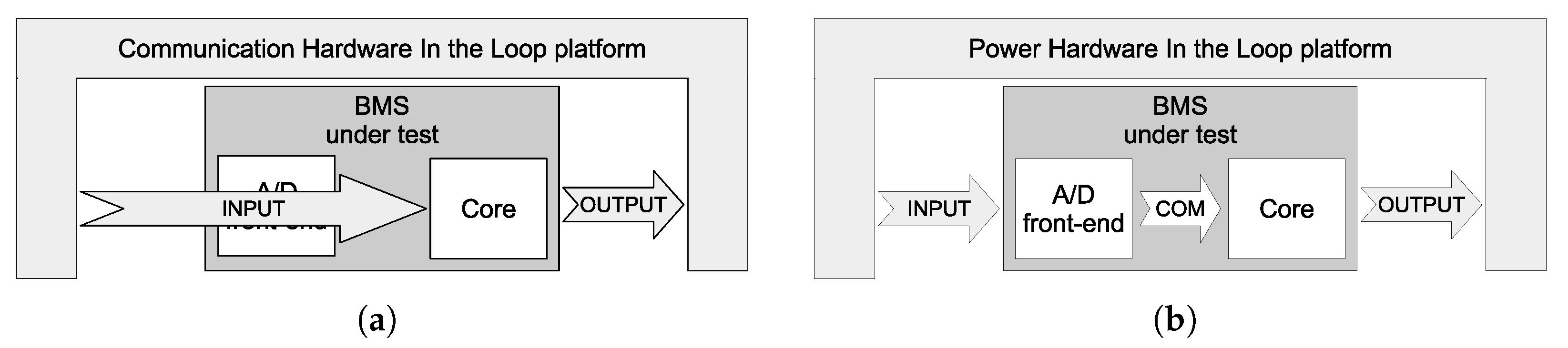
2. Background
3. Cell Emulator Constraints
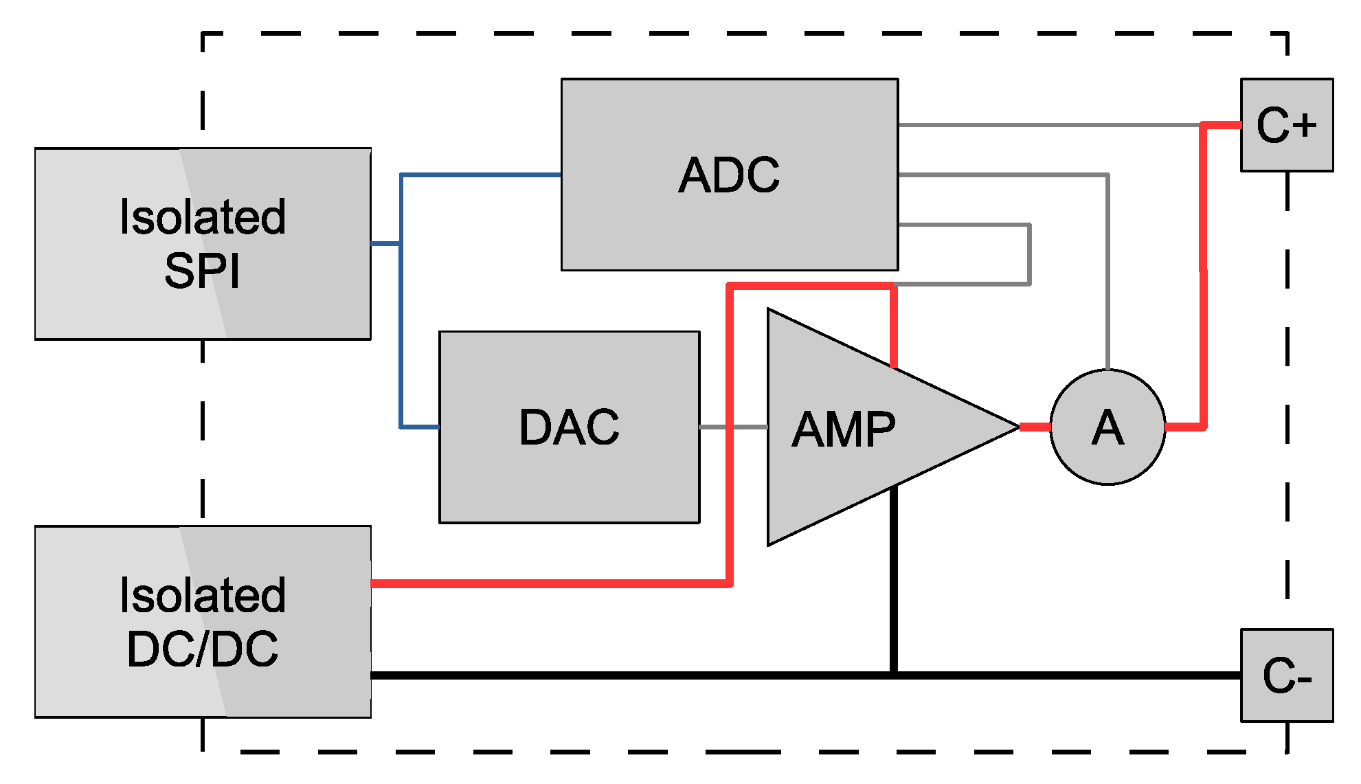
4. Cell Emulator Circuit Design
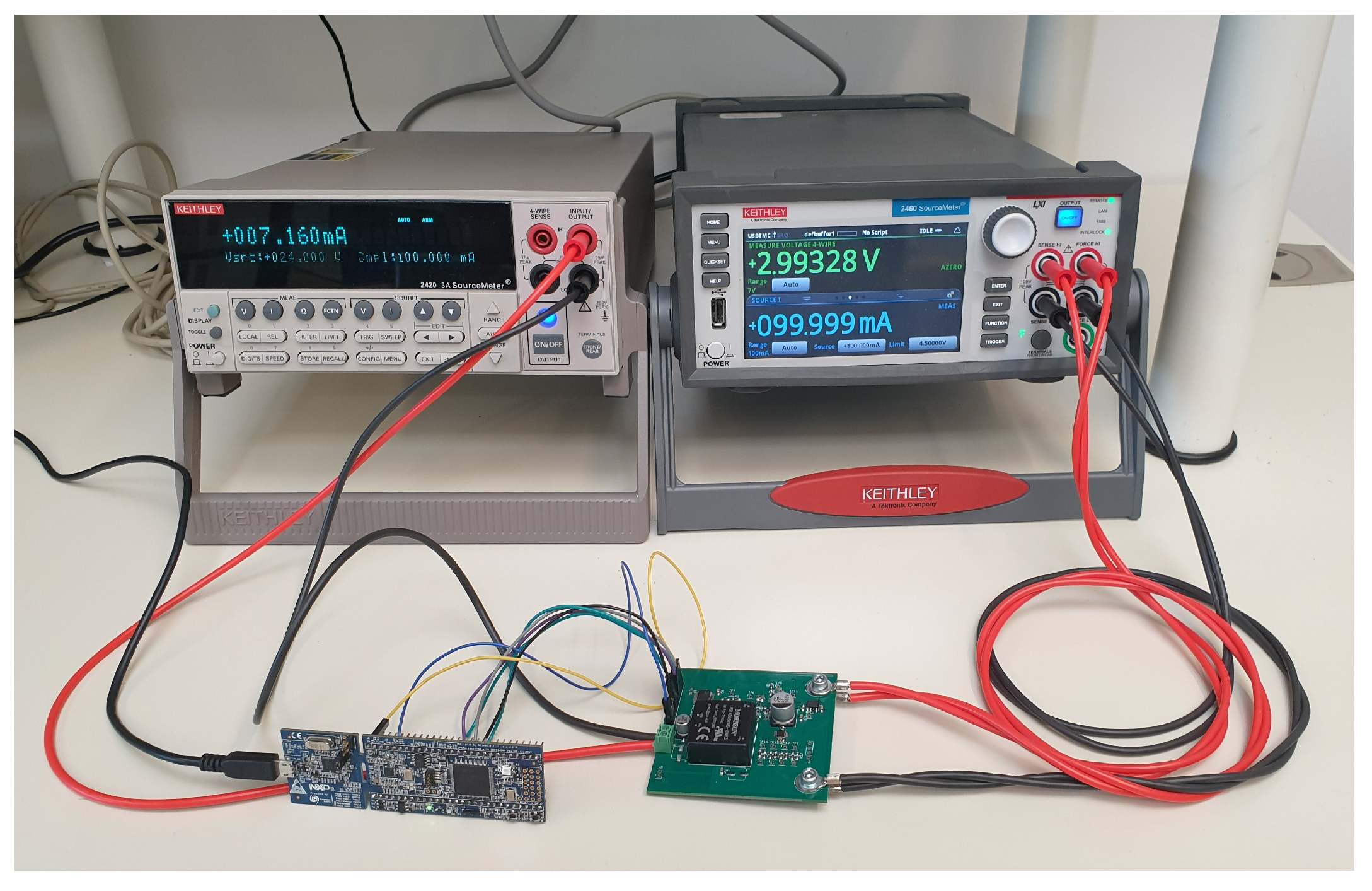
5. Experimental Characterization of the Cell Emulator
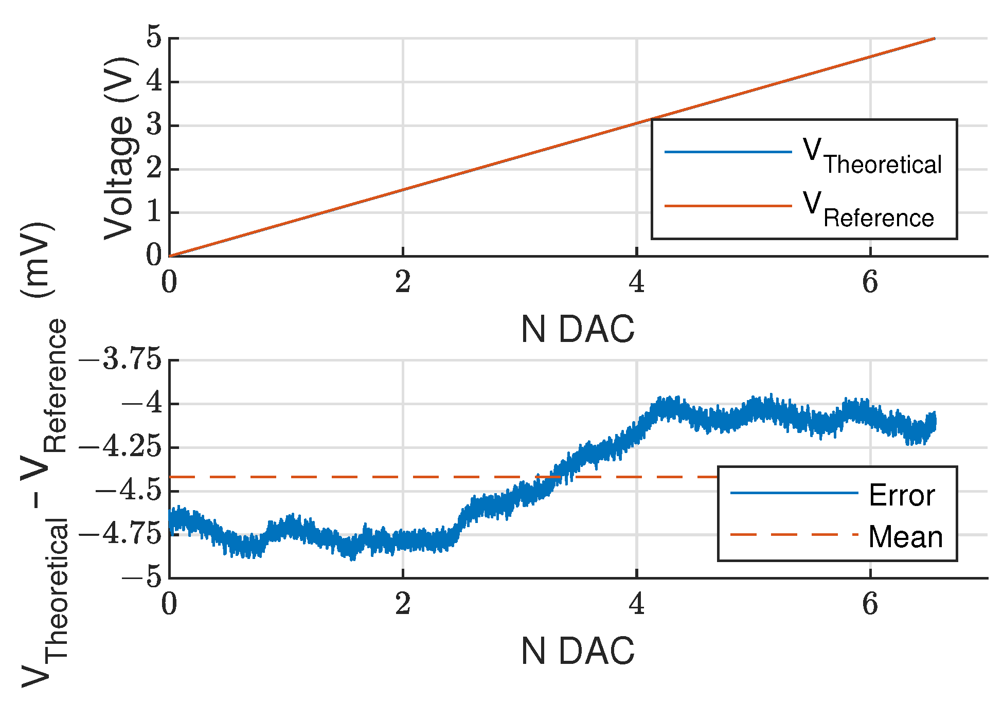
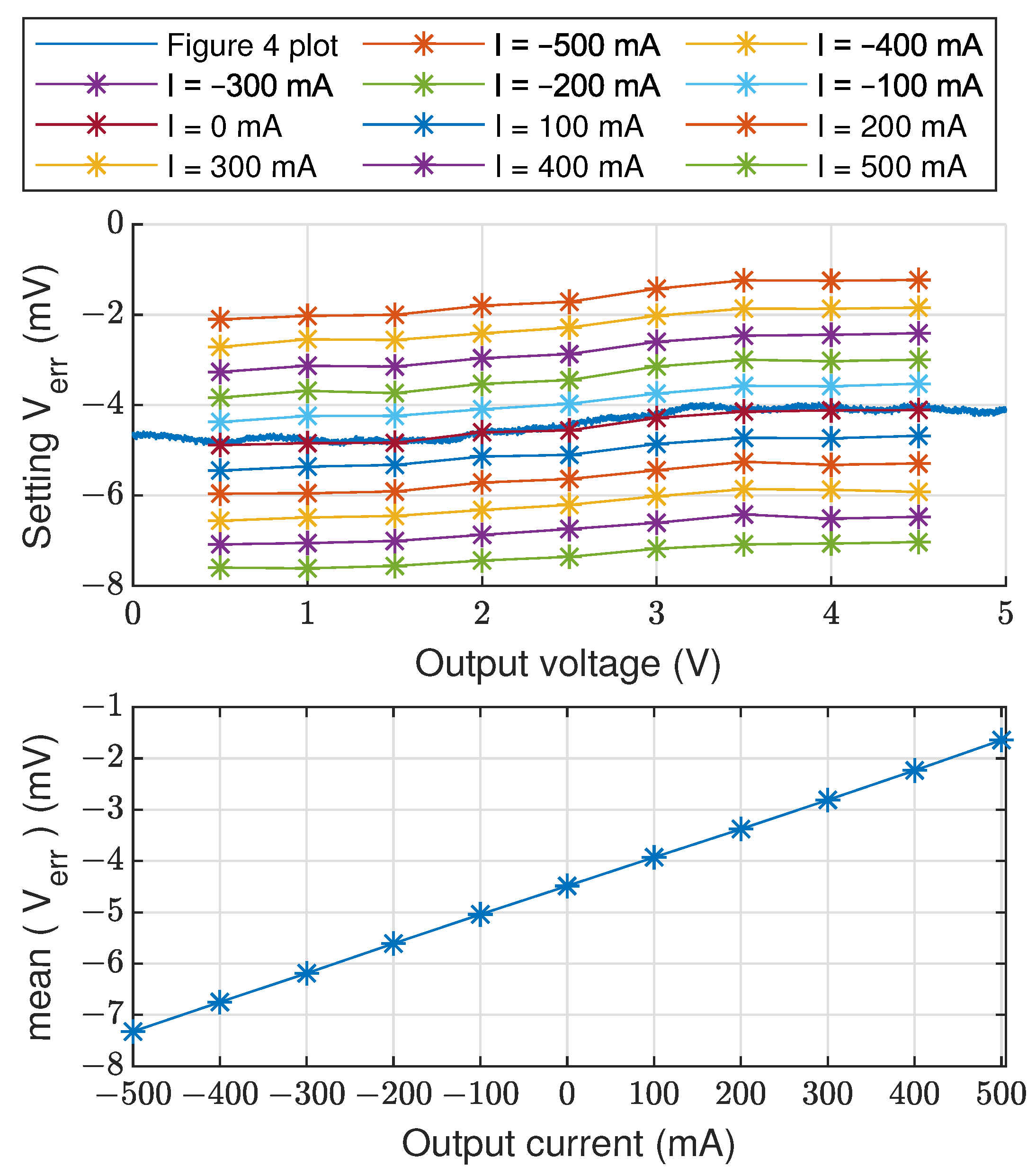
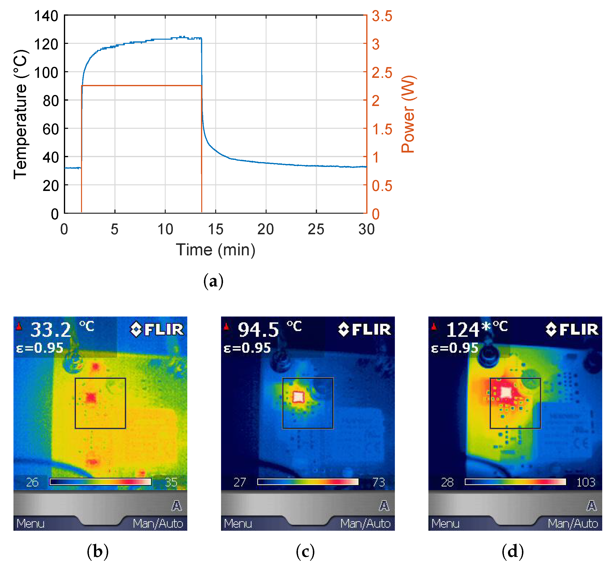
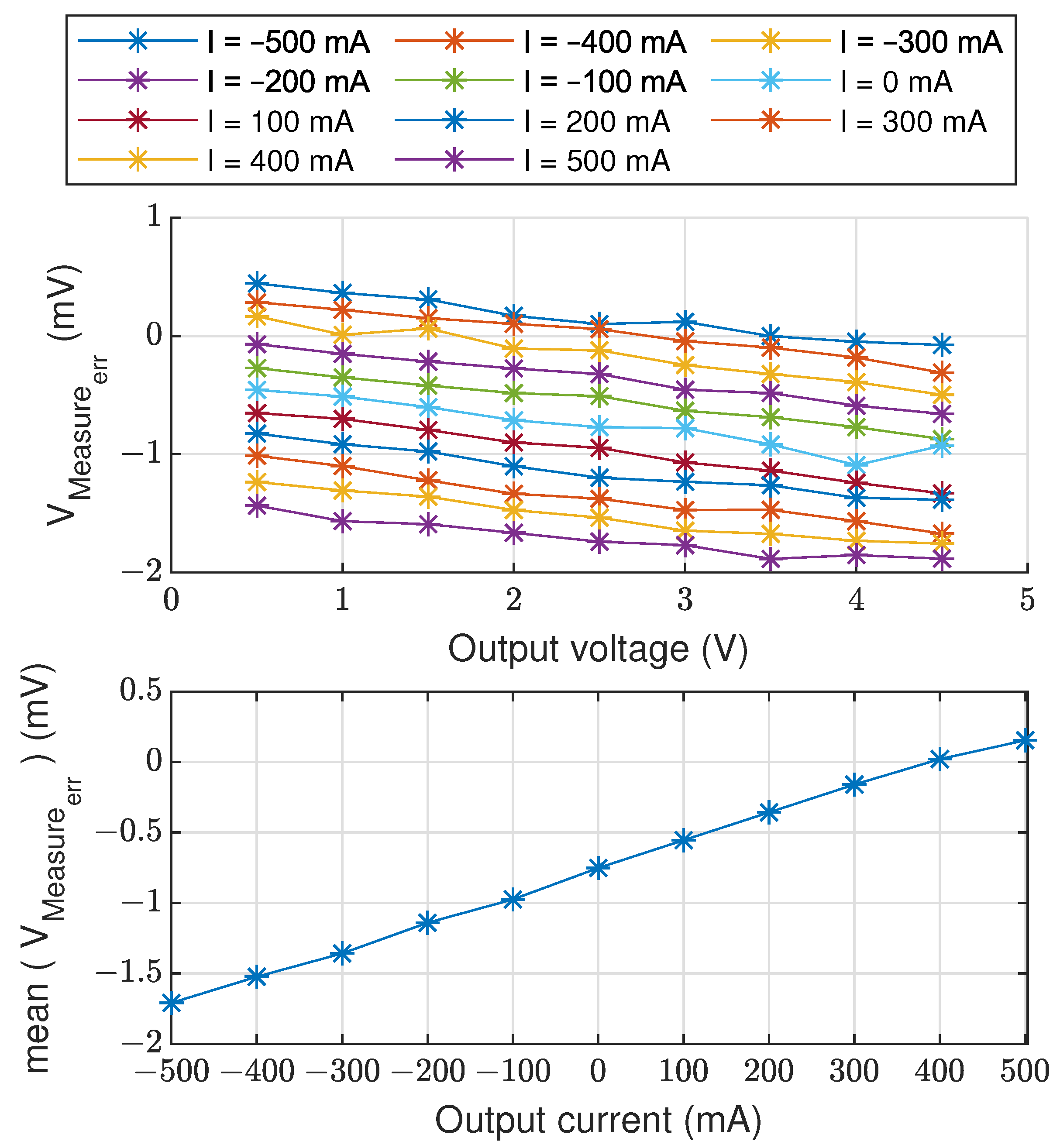
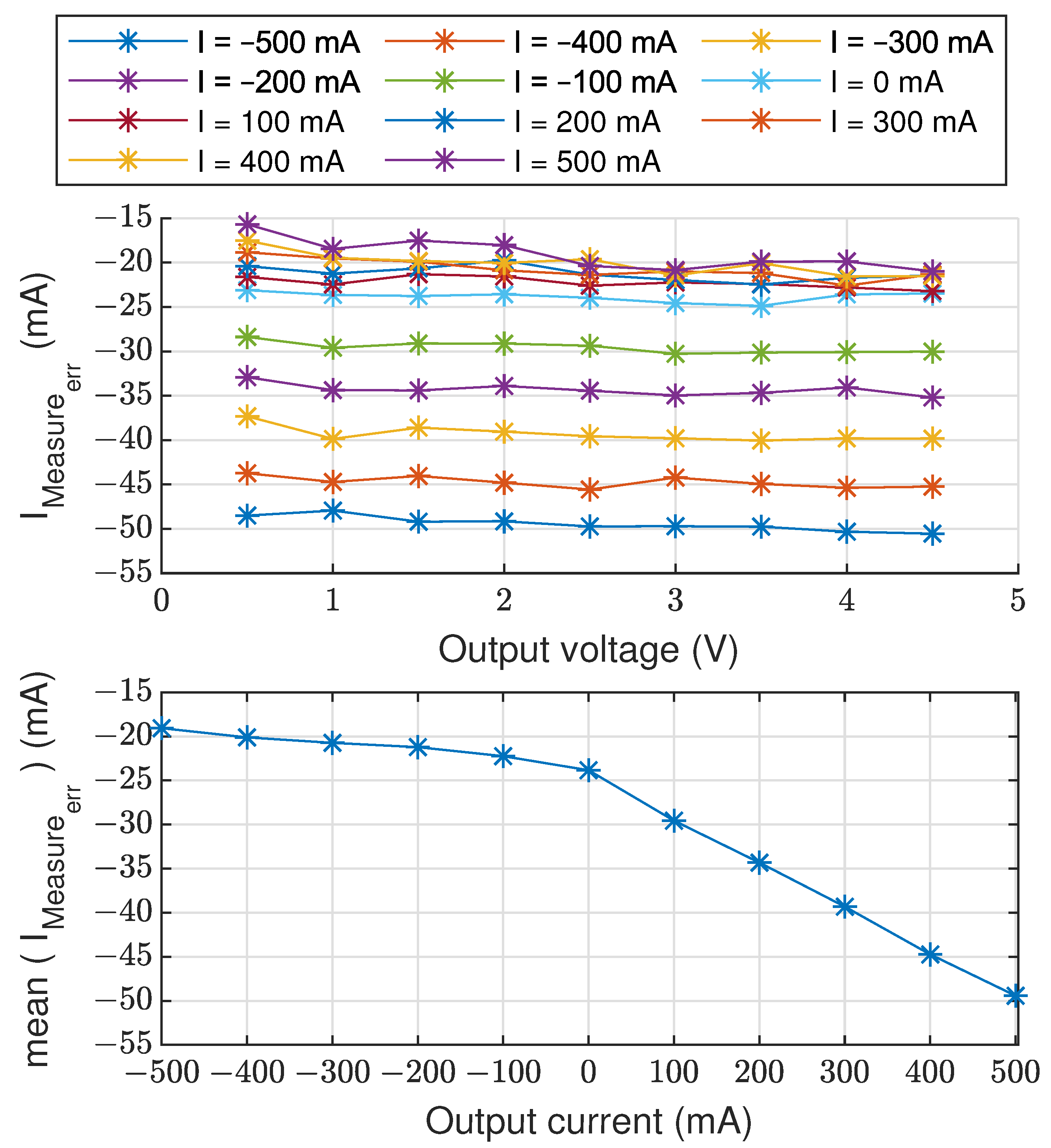
5.1. Characterization Test Results for the Emulator Cell #1
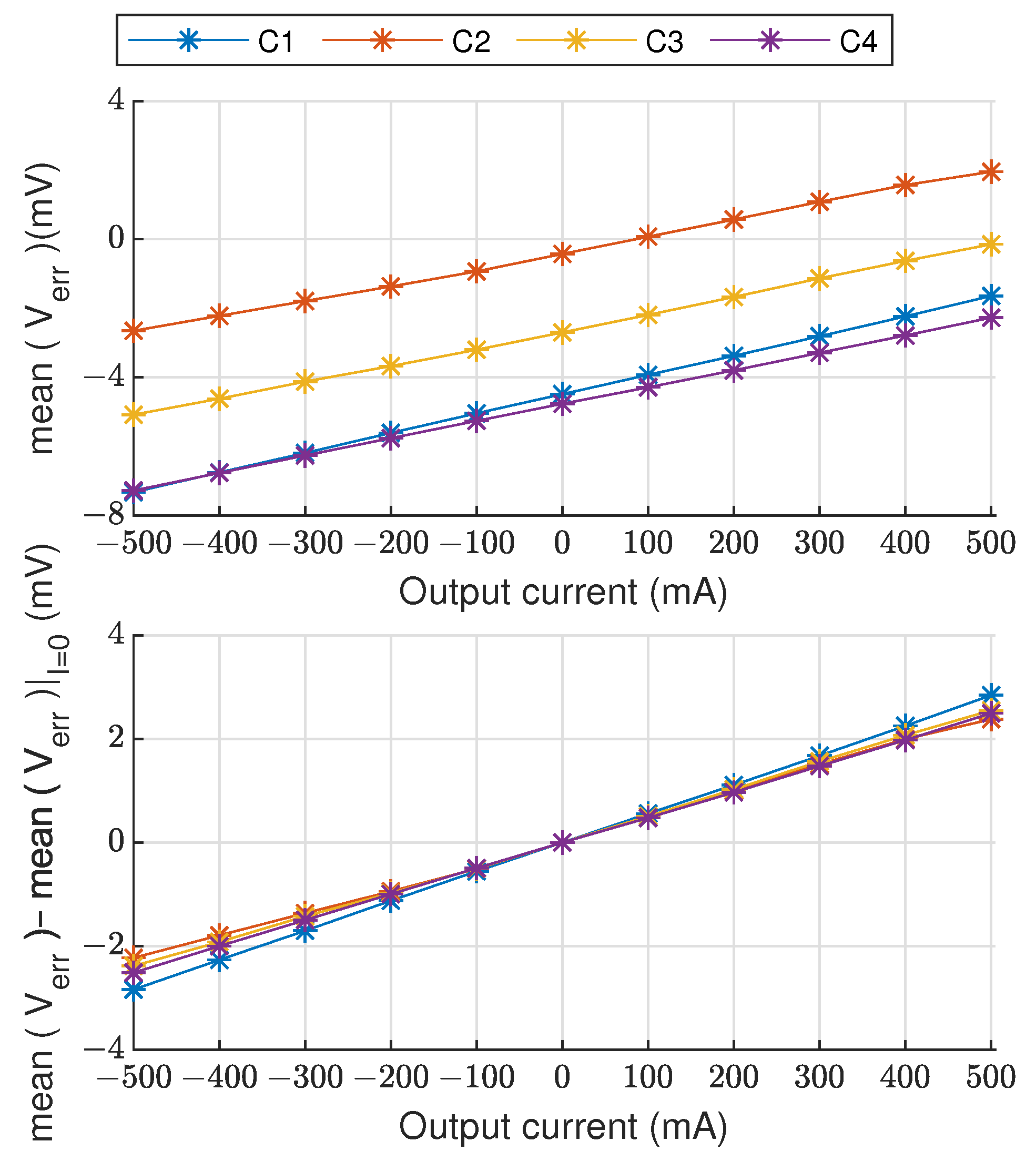
5.2. Comparison of 4 Cell Emulator Instances
6. Discussion and Future Developments
7. Conclusions
Author Contributions
Funding
Acknowledgments
Conflicts of Interest
References
- Wu, H. Hardware-in-loop verification of battery management system. In Proceedings of the 2011 4th International Conference on Power Electronics Systems and Applications, Hong Kong, China, 8–10 June 2011. [Google Scholar] [CrossRef]
- Barreras, J.V.; Fleischer, C.; Christensen, A.E.; Swierczynski, M.; Schaltz, E.; Andreasen, S.J.; Sauer, D.U. An Advanced HIL Simulation Battery Model for Battery Management System Testing. IEEE Trans. Ind. Appl. 2016, 52, 5086–5099. [Google Scholar] [CrossRef]
- Morello, R.; Baronti, F.; Tian, X.; Chau, T.; Di Rienzo, R.; Roncella, R.; Jeppesen, B.; Lin, W.H.; Ikushima, T.; Saletti, R. Hardware-in-the-loop simulation of FPGA-based state estimators for electric vehicle batteries. In Proceedings of the IEEE International Symposium on Industrial Electronics, Santa Clara, CA, USA, 8–10 June 2016; pp. 280–285. [Google Scholar] [CrossRef]
- Tschritter, C.D.; Wetz, D.A.; Turner, G.K.; Heinzel, J.M. Battery Management System (BMS) Test Stand Utilizing a Hardware-in-the-Loop (HIL) Emulated Battery. In Proceedings of the 2021 IEEE Electric Ship Technologies Symposium (ESTS), Arlington, TX, USA, 3–6 August 2021. [Google Scholar] [CrossRef]
- Bui, T.M.; Niri, M.F.; Worwood, D.; Dinh, T.Q.; Marco, J. An Advanced Hardware-in-the-Loop Battery Simulation Platform for the Experimental Testing of Battery Management System. In Proceedings of the 2019 23rd International Conference on Mechatronics Technology (ICMT), Salerno, Italy, 23–26 October 2019. [Google Scholar] [CrossRef] [Green Version]
- Mishra, S.; Tamballa, S.; Pallantala, M.; Raju, S.; Mohan, N. Cascaded Dual-Active Bridge Cell Based Partial Power Converter for Battery Emulation. In Proceedings of the 2019 20th Workshop on Control and Modeling for Power Electronics (COMPEL), Toronto, ON, Canada, 17–20 June 2019. [Google Scholar] [CrossRef]
- Di Rienzo, R.; Roncella, R.; Morello, R.; Baronti, F.; Saletti, R. Low-cost modular battery emulator for battery management system testing. In Proceedings of the 2018 IEEE International Conference on Industrial Electronics for Sustainable Energy Systems (IESES), Hamilton, New Zealand, 31 January–2 February 2018; pp. 44–49. [Google Scholar] [CrossRef] [Green Version]
- Van Sterkenburg, S.; Fleuren, T.; Veenhuizen, B.; Groenewegen, J. Design and test of a battery pack simulator. In Proceedings of the 2013 World Electric Vehicle Symposium and Exhibition (EVS27), Barcelona, Spain, 17–20 November 2013. [Google Scholar] [CrossRef]
- Collet, A.; Crebier, J.C.; Chureau, A. Multi-cell battery emulator for advanced battery management system benchmarking. In Proceedings of the 2011 IEEE International Symposium on Industrial Electronics, Gdansk, Poland, 27–30 June 2011; pp. 1093–1099. [Google Scholar] [CrossRef]
- Buccolini, L.; Orcioni, S.; Longhi, S.; Conti, M. Cell Battery Emulator for Hardware-in-the-Loop BMS Test. In Proceedings of the 2018 IEEE International Conference on Environment and Electrical Engineering and 2018 IEEE Industrial and Commercial Power Systems Europe (EEEIC/ICPS Europe), Palermo, Italy, 12–15 June 2018. [Google Scholar] [CrossRef]
- Bischof, S.; Kuecuek, C.; Blank, T.; Weber, M. A battery cell emulator for hardware in the loop tests of reconfigurable lithium-ion and post-lithium batteries. In Proceedings of the PCIM Europe 2018; International Exhibition and Conference for Power Electronics, Intelligent Motion, Renewable Energy and Energy Management, Nuremberg, Germany, 5–7 June 2018; pp. 245–251. [Google Scholar]
- Morello, R.; Zamboni, W.; Baronti, F.; Di Rienzo, R.; Roncella, R.; Spagnuolo, G.; Saletti, R. Comparison of state and parameter estimators for electric vehicle batteries. In Proceedings of the IECON 2015-41st Annual Conference of the IEEE Industrial Electronics Society, Yokohama, Japan, 9–12 November 2015; pp. 5433–5438. [Google Scholar] [CrossRef]
- Zhang, M.; Wang, K.; Zhou, Y.T. Online state of charge estimation of lithium-ion cells using particle filter-based hybrid filtering approach. Complexity 2020, 2020, 8231243. [Google Scholar] [CrossRef]
- Li, Q.; Li, D.; Zhao, K.; Wang, L.; Wang, K. State of health estimation of lithium-ion battery based on improved ant lion optimization and support vector regression. J. Energy Storage 2022, 50, 104215. [Google Scholar] [CrossRef]
- Modular Battery Emulator. Available online: https://github.com/batterylabunipi/Modular_Battery_Emulator (accessed on 18 February 2022).
- Carloni, A.; Baronti, F.; Di Rienzo, R.; Roncella, R.; Saletti, R. Open and Flexible Li-ion Battery Tester Based on Python Language and Raspberry Pi. Electronics 2018, 7, 454. [Google Scholar] [CrossRef] [Green Version]
- Morello, R.; Di Rienzo, R.; Roncella, R.; Saletti, R.; Baronti, F. Hardware-in-the-loop platform for assessing battery state estimators in electric vehicles. IEEE Access 2018, 6, 68210–68220. [Google Scholar] [CrossRef]
- Vereb, S.; Balazs, G.G.; Kokenycsi, T.; Suto, Z.; Varjasi, I. Application Dependent Optimization of Balancing Methods for Lithium-ion Batteries. In Proceedings of the 2018 IEEE 18th International Power Electronics and Motion Control Conference (PEMC), Budapest, Hungary, 26–30 August 2018; pp. 223–228. [Google Scholar] [CrossRef]
- Chen, M.; Rincon-Mora, G.A. Accurate Electrical Battery Model Capable of Predicting Runtime and I-V Performance. IEEE Trans. Energy Convers. 2006, 21, 504–511. [Google Scholar] [CrossRef]
- Tarascon, J.M.; Armand, M. Issues and challenges facing rechargeable lithium batteries. Nature 2001, 414, 359–367. [Google Scholar] [CrossRef] [PubMed]
- Di Rienzo, R.; Zeni, M.; Baronti, F.; Roncella, R.; Saletti, R. Passive balancing algorithm for charge equalization of series connected battery cells. In Proceedings of the 2020 2nd IEEE International Conference on Industrial Electronics for Sustainable Energy Systems (IESES), Cagliari, Italy, 1–3 September 2020; pp. 73–79. [Google Scholar] [CrossRef]
- Ghotekar, A.A.; Kushare, B.E. Review paper on recent active voltage balancing methods for supercapacitor energy storage system. In Proceedings of the 2019 5th International Conference On Computing, Communication, Control And Automation (ICCUBEA), Pune, India, 19–21 September 2019. [Google Scholar] [CrossRef]
- KiCad EDA-Schematic Capture PCB Design Software. Available online: https://www.kicad.org/ (accessed on 18 February 2022).


| Feature | Requirement |
|---|---|
| Voltage range | 0.5 to |
| Voltage resolution | ≈76 μV |
| Voltage update frequency | ≥100 |
| Maximum continuous source/sink current |
| Work | [5] | [9] | [10] | Our Work |
|---|---|---|---|---|
| Cell Architecture | Commercial (dSpace HIL) | OPAMP µC with internal 12b DAC/ADC | OPAMP µC with external 16b DAC/ADC | OPAMP 16b DAC/ADC |
| Voltage resolution | 120 μV | 1.2 mV 2 | 92 μV 3 | 76 μV |
| Voltage accuracy | ±1 | ±270 μV | ±2.17 | |
| Max Current | 2 | 3–5 | 3 | |
| Current accuracy | NS | 2 | ±462 μA | ±19.6 |
| set time | 31.25 μs | 5 μs | 1.26 μs | 340 μs |
| cost | very high | low | medium | very low |
Publisher’s Note: MDPI stays neutral with regard to jurisdictional claims in published maps and institutional affiliations. |
© 2022 by the authors. Licensee MDPI, Basel, Switzerland. This article is an open access article distributed under the terms and conditions of the Creative Commons Attribution (CC BY) license (https://creativecommons.org/licenses/by/4.0/).
Share and Cite
Di Rienzo, R.; Verani, A.; Baronti, F.; Roncella, R.; Saletti, R. Modular Battery Emulator for Development and Functional Testing of Battery Management Systems: The Cell Emulator. Electronics 2022, 11, 1215. https://doi.org/10.3390/electronics11081215
Di Rienzo R, Verani A, Baronti F, Roncella R, Saletti R. Modular Battery Emulator for Development and Functional Testing of Battery Management Systems: The Cell Emulator. Electronics. 2022; 11(8):1215. https://doi.org/10.3390/electronics11081215
Chicago/Turabian StyleDi Rienzo, Roberto, Alessandro Verani, Federico Baronti, Roberto Roncella, and Roberto Saletti. 2022. "Modular Battery Emulator for Development and Functional Testing of Battery Management Systems: The Cell Emulator" Electronics 11, no. 8: 1215. https://doi.org/10.3390/electronics11081215