1. Introduction
The center-tap rectifier (CTR) without an output inductor is widely used in many switching converters in low output-voltage and high output-current applications, since it has a simple structure, low voltage stresses, and small conduction losses resulting from two diodes in the secondary side. The asymmetric/symmetric half-bridge (HB) and full-bridge (FB) converters with pulse-width modulation (PWM) control and resonant converters with pulse-frequency modulation (PFM) control normally adopt the CTR for the DC/DC power conversion. The CTR has many advantages, such as a simple structure, low component count, and flexibility in designing an asymmetric turns-ratio between the secondary turns. However, it has a limitation in making high input/output (I/O) voltage gain, due to a disadvantageous transformer turns-ratio. For example, if an HB LLC resonant converter, as shown in
Figure 1a, operates in a resonant region, the voltage (V
M) on the magnetizing inductor (L
M) of the center-tap transformer is half of the input voltage (V
S/2), and is transferred to the output (V
O) through the transformer turns-ratio (n), i.e., V
O = V
S/(2n), i.e., n = N
P/N
S.
To relieve this drawback, the voltage doubler rectifier (VDR) in
Figure 1b is frequently used in many applications requiring a higher transformer turns-ratio (n). For example, if an HB LLC resonant converter with the VDR operates in a resonant region, the voltage (V
M) on the magnetizing inductor (L
M) of the transformer with the VDR is half of the input voltage (V
S/2), and is transferred to the voltage (V
D) on a doubler capacitor (C
D) through the transformer turns-ratio (n), i.e., V
D = V
S/(2n). Since the output voltage (V
O) is the sum of V
D and the voltage (V
NS) across the secondary turn (N
S), i.e., V
NS = V
S/(2n) and V
O = V
D + V
NS, V
O is V
S/n, which means that n can be doubled, compared with the center-tap transformer in
Figure 1a.
In addition, there are several approaches to obtain a higher I/O voltage gain [
1,
2,
3,
4,
5,
6,
7,
8].
Table 1 shows comparisons with “prior arts.” In column [
1] of
Table 1, the HB LLC resonant converter can achieve a higher I/O voltage gain by increasing the transformer secondary turns. However, it utilizes one additional diode and switch, and additional transformer secondary windings, which cause circuit complexity. Moreover, in the mode of increasing I/O voltage gain, the offset current in the transformer occurs due to the primary unbalanced current, which results from only one powering operation in the secondary side. The offset current in the transformer causes the size of the transformer to be increased. In column [
2] of
Table 1, the HB LLC converter with a boost pulse-width modulation (PWM) control method is proposed. In the mode of increasing I/O voltage gain, the added switch is turned on or off with PWM control. While the added switch is turned on, the energy stored in the resonant capacitor (C
r) is stored in the resonant inductor (L
r) by the resonance between L
r and C
r. Meanwhile, if the added switch is turned off, the energy stored in L
r is transferred to the output through the transformer; thus, a higher I/O voltage gain can be obtained. However, one additional switch is needed, and the additional switch cannot be clamped due to the leakage inductor of the transformer, which has high voltage stress. Moreover, as in column [
1] in
Table 1, the offset current in the transformer occurs due to the primary unbalanced current, which results from only one powering operation in the secondary side. This increases the transformer size. In column [
3] of
Table 1, the HB LLC converter with the asymmetric PWM control method is proposed. This paper does not consider additional devices in order to obtain higher I/O voltage gain. However, in a situation of obtaining higher I/O voltage gain, asymmetric PWM control is used. Since it causes “only one powering operation during small duty-cycle” in one switching period, the primary current becomes unbalanced; thus, the offset current in the transformer occurs. The offset current in the transformer causes the size of the transformer to be increased, similar to [
1,
2].
In column [
4] of
Table 1, a boost converter, which is utilized as a power factor correction (PFC) stage, is used to obtain higher I/O voltage gain. For higher I/O voltage gain, the boost inductor (L
B) in the PFC stage is replaced with a coupled inductor with secondary winding in the secondary side of the DC/DC stage, and one diode (D
A) and switch (Q
A) are added in the secondary side of the DC/DC stage. In a situation of obtaining higher I/O voltage gain, the HB flyback converter with a single-ended rectifier is operated with a coupled inductor in the PFC stage and one diode and switch in the secondary side, finishing the operation of main HB LLC converter. This does not have offset current in the transformer, but too many components would be additionally required. In column [
5] of
Table 1, the HB LLC converter is proposed with additional “one primary switch (Q
A)” and “one resonant tank”, including one transformer and a resonant inductor and a capacitor. If higher I/O voltage gain is required, an additional primary switch (Q
A) is always turned on, and Q
P1 and Q
P2 are alternatively switched. In this case, since the input voltage (V
S) is applied to each transformer in two “parallel-connected” resonant tanks, high I/O voltage gain can be obtained. Meanwhile, if Q
P1 and Q
P2 are together turned on or off, alternatively with Q
A, two transformers in two resonant tanks are connected in series. Since half (V
S/2) of the input voltage is applied to each transformer, low I/O voltage gain is achieved. This does not have offset current in the transformer, but too many components would be additionally required. In column [
6] of
Table 1, the HB LLC converter is proposed by “replacing two diodes with two switches” and “applying phase-shifted control” in the secondary full-bridge rectifier. If higher I/O voltage gain is needed, the phase-shifted control between the primary switches (Q
1 and Q
2) and the secondary switches (SR
1 and SR
2) is applied. Since the energy stored in a resonant inductor (L
r) is further increased, as the free-wheeling period in the secondary side is larger, higher I/O voltage gain can be achieved. However, this cannot be applied in a center-tapped rectifier, but only in a full-bridge rectifier. Moreover, this requires two additional secondary switches. In column [
7] in
Table 1, the HB LLC converter is proposed by “adding one switch (Q
A) and one resonant capacitor (C
RA)”. If higher I/O voltage gain is required, the additional switch is turned on; thus, the resonant capacitance is increased. Since Q factor is reduced, higher I/O voltage gain can be achieved. However, this requires additional on/off control and additional devices, which cause the complexity of the system. In column [
8] of
Table 1, the HB LLC converter is proposed by “replacing two diodes with two switches (Q
SR1 and Q
SR2)” and “adding one blocking capacitor (C
B)” in the secondary full-bridge rectifier. In the “normal full-bridge control” in the secondary side, an additional blocking capacitor (C
B) has only a function of current-balancing during the resonant region operation. Meanwhile, if higher I/O voltage gain is needed, low-side switches in the secondary full-bridge legs are both turned on. During this period, an additional blocking capacitor (C
B) stores V
S/(2 × n), where Vs and n, respectively, indicate the input voltage and the transformer turns-ratio. Then, the V
S/(2 × n) stored in the C
B is transferred to the output, with the transformer voltage reflected in the secondary side, i.e., V
S/(2 × n). Thus, the proposed converter in column [
8] of
Table 1 can obtain higher I/O voltage gain. However, this requires complex secondary gate control and two switches, which cannot be applied in a center-tapped rectifier but only in a full-bridge rectifier.
In this paper, new rectifiers to obtain higher voltage gain are proposed; a voltage tripler rectifier and a voltage quadrupler rectifier, which require one more capacitor in the secondary side compared with the CTR, or no elements compared with the VDR. Moreover, compared with columns [
1,
2,
4,
5,
6,
7,
8] in
Table 1, the proposed rectifiers can achieve high I/O voltage gain with “smaller number of elements.” In addition, although the proposed voltage tripler has a “transformer offset current,” it has a very small transformer offset current compared with columns [
1,
2,
3] in
Table 1, due to the “large transformer turns-ratio” resulting from higher I/O voltage gain. Meanwhile, the proposed voltage quadrupler has no transformer offset current. As a result, the proposed rectifiers can have a small volume, due to the low component count and the small-sized transformer, compared with prior arts. They have a simple structure with one capacitor and two diodes, and three and four times higher voltage gain with the same transformer turns-ratio.
The validity of these proposed rectifiers in the half-bridge (HB) LLC resonant converter is verified by the experimental results from a 100 W/200 V output prototype.
2. Comparison and Analysis
Figure 1 shows the circuit diagram of the conventional and proposed rectifiers.
Figure 1a,b show the CTR and VDR, respectively. The CTR in
Figure 1a has two secondary turns (N
S1 and N
S2), and two diodes are series-connected to each turn.
Meanwhile, the VDR in
Figure 1b has a secondary turn (N
S), and the doubler capacitor (C
D) is series-connected to that. If the secondary current (i
Sec) reflected from the primary flows in the secondary undot direction, the secondary diode (D
S2) is conducted. During this interval, assuming resonant operation, since half of the input voltage (V
S/2) is applied to L
M in the primary undot direction, V
S/(2n) is applied to N
S in the undot direction, and the voltage (V
D) on C
D is V
S/(2n). Since V
O is V
S/n in the VDR in resonant operation, as explained in
Section 1, V
D is V
O/2, i.e., V
D = V
S/(2n) = V
O/2. On the other hand, if the secondary current (i
Sec) reflected from the primary flows in the secondary dot direction, the secondary diode (D
S1) is conducted, and the i
sec flows through N
S, D
S1, and C
D. During this interval, assuming resonant operation, since half of the input voltage (V
S/2) is applied to L
M in the primary dot direction, V
S/(2n) is applied to N
S in the dot direction. Since the output voltage (V
O) is the sum of V
D and the voltage (V
NS) across the secondary turn (N
S), i.e., V
NS = V
S/(2n) and V
O = V
D + V
NS, V
O is V
S/n. Thus, two times higher input/output (I/O) voltage gain can be achieved with an equal turns-ratio, compared with the CTR in
Figure 1a.
On the other hand,
Figure 1c and
Figure 1d show the proposed voltage tripler and quadrupler, respectively, and
Figure 2 shows their operational modes. To achieve higher I/O voltage gain, the proposed rectifier has new secondary windings from the VDR.
The voltage tripler has a new N
S2, which is series-connected with D
S2. If the secondary current (i
Sec) reflected from the primary flows in the secondary undot direction, the secondary diode (D
S2) is conducted, and the secondary current flows through N
S1, C
D, D
S2, and N
S2, as shown in
Figure 2a. During this interval, assuming resonant operation, since half of the input voltage (V
S/2) is applied to L
M in the primary undot direction, V
S/(2n) is applied, respectively, to N
S1 and N
S2 in the undot direction, and the voltage (V
D) on C
D is V
S/n. On the other hand, if the secondary current (i
Sec) reflected from the primary flows in the secondary dot direction, the secondary diode (D
S1) is conducted, the i
sec flows through N
S1, D
S1, and C
D., and D
S2 is blocked, as shown in
Figure 2b. During this interval, assuming resonant operation, since half of the input voltage (V
S/2) is applied to L
M in the primary dot direction, V
S/(2n) is applied to N
S1 in the dot direction. Since the output voltage (V
O) is the sum of V
D and the voltage (V
NS1) across the secondary turn (N
S1), i.e., V
NS1 = V
S/(2n) and V
O = V
D + V
NS1, V
O is 3V
S/(2n). That is, since V
D is V
S/n, V
D is equal to 2V
O/3.
The voltage quadrupler is operated similarly to the voltage tripler. It has new windings N
S2 and N
S3, which are series-connected with D
S2 and D
S1, respectively. If the secondary current (i
Sec) reflected from the primary flows in the secondary undot direction, the secondary diode (D
S2) is conducted, and the secondary current flows through N
S1, C
D, D
S2, and N
S2, as shown in
Figure 2c. During this interval, assuming resonant operation, since half of the input voltage (V
S/2) is applied to L
M in the primary undot direction, V
S/(2n) is respectively applied to N
S1 and N
S2 in the undot direction, and the voltage (V
D) on C
D is V
S/n. On the other hand, if the secondary current (i
Sec) reflected from the primary flows in the secondary dot direction, the secondary diode (D
S1) is conducted, the i
sec flows through N
S1, N
S3, D
S1, and C
D., and D
S2 is blocked, as shown in
Figure 2d. During this interval, assuming resonant operation, since half of the input voltage (V
S/2) is applied to L
M in the primary dot direction, V
S/(2n) is respectively applied to N
S1 and N
S3 in the dot direction. Since the output voltage (V
O) is the sum of V
D and voltages (V
NS1 and V
NS3) across the secondary turns (N
S1 and N
S3), i.e., V
NS1 = V
NS3 = V
S/(2n) and V
O = V
D + V
NS1 + V
NS3, V
O is 2V
S/n. That is, since V
D is V
S/n, V
D is equal to V
O/2.
Consequently, in the proposed voltage tripler and quadrupler, three and four times higher input/output (I/O) voltage gain can be achieved with an equal turns-ratio, compared with the CTR shown in
Figure 1a.
Table 2 and
Table 3 show the comparison of rectifiers in terms of the transformer turns-ratio, the voltage and RMS current of C
D, and the voltage and current stresses of D
S1 and D
S2. It is assumed that the HB LLC resonant converter operates in a resonant region, the diodes (D
S1 and D
S2) have the same conduction time, N
P is the transformer primary turns, and the rectifiers have equal output voltage (V
O) and output current (I
O).
2.1. Transformer Turns-Ratio and Magnetizing Offset Current
Since the I/O voltage gains of the conventional CTR and VDR and the proposed tripler and quadrupler rectifiers are, respectively, VS/(2n), VS/n, 3VS/(2n), and 2VS/n, the turns-ratios (n = NP/NSk, k = 1, 2, 3) of the VDR and the tripler and quadrupler rectifiers are 2, 3, and 4, respectively, under n = 1 in the CTR. Thus, a larger turns-ratio (n = NP/NS) is required to obtain the same output voltage in the proposed tripler and quadrupler, compared with the CTR and the VDR.
Meanwhile, in the HB LLC resonant converter with the CTR, the secondary resonant current is flowing alternately in the secondary dot or undot direction during half of a switching period (T
S/2), and their average should be the output current (I
O). Thus, each average of the i
Sec flowing in the secondary dot or undot direction should be half of the output current (I
O/2). If the i
sec is reflected in the primary side of the transformer, each average of the reflected primary current (i
Pri,
Rf) is I
O/(2n) or −I
O/(2n) during T
S/2, as shown in
Figure 3a. Due to the current-second balance on the primary resonant capacitor, the transformer magnetizing offset current is zero in the CTR. In
Figure 3, M
1 and M
2, respectively, indicate operational modes 1 and 2.
Second, in the VDR, the secondary resonant current, which only flows in the secondary dot direction, is transferred to the output through C
D during T
S/2, and its average should be the output current (I
O). Meanwhile, the secondary resonant current, flowing in the secondary undot direction, does not pass through the output, but through C
D and D
S2. Due to the current-second balance on C
D, its average should be −I
O during the undot-direction operation. If the i
sec is reflected in the primary side of the transformer, each average of the reflected primary current (i
Pri,
Rf) is I
O/n or −I
O/n during T
S/2, as shown in
Figure 3b. Due to the current-second balance on the primary resonant capacitor, the transformer magnetizing offset current is also zero in the VDR.
Third, in the proposed tripler rectifier, the secondary resonant current (i
Sec = i
DS1), which only flows in the secondary dot direction of N
S1, is transferred to the output through C
D and D
S1 during T
S/2, as shown in
Figure 2b, and its average should be the output current (I
O), as shown in
Figure 3c. Meanwhile, the secondary resonant current, flowing in the secondary undot direction of N
S1 and N
S2, does not pass through the output, but through C
D and D
S2, as shown in
Figure 2a. Due to the current-second balance on C
D, its average should be −I
O during the undot-direction operation. If the i
sec is reflected in the primary side of the transformer, the average of the reflected primary current (i
Pri,
Rf) in the dot direction is I
O/n, and the average of i
Pri,
Rf in the undot direction is −2I
O/n, as shown in
Figure 3c. Due to the current-second balance on the primary resonant capacitor, the transformer magnetizing offset current is I
O/n in the proposed tripler rectifier.
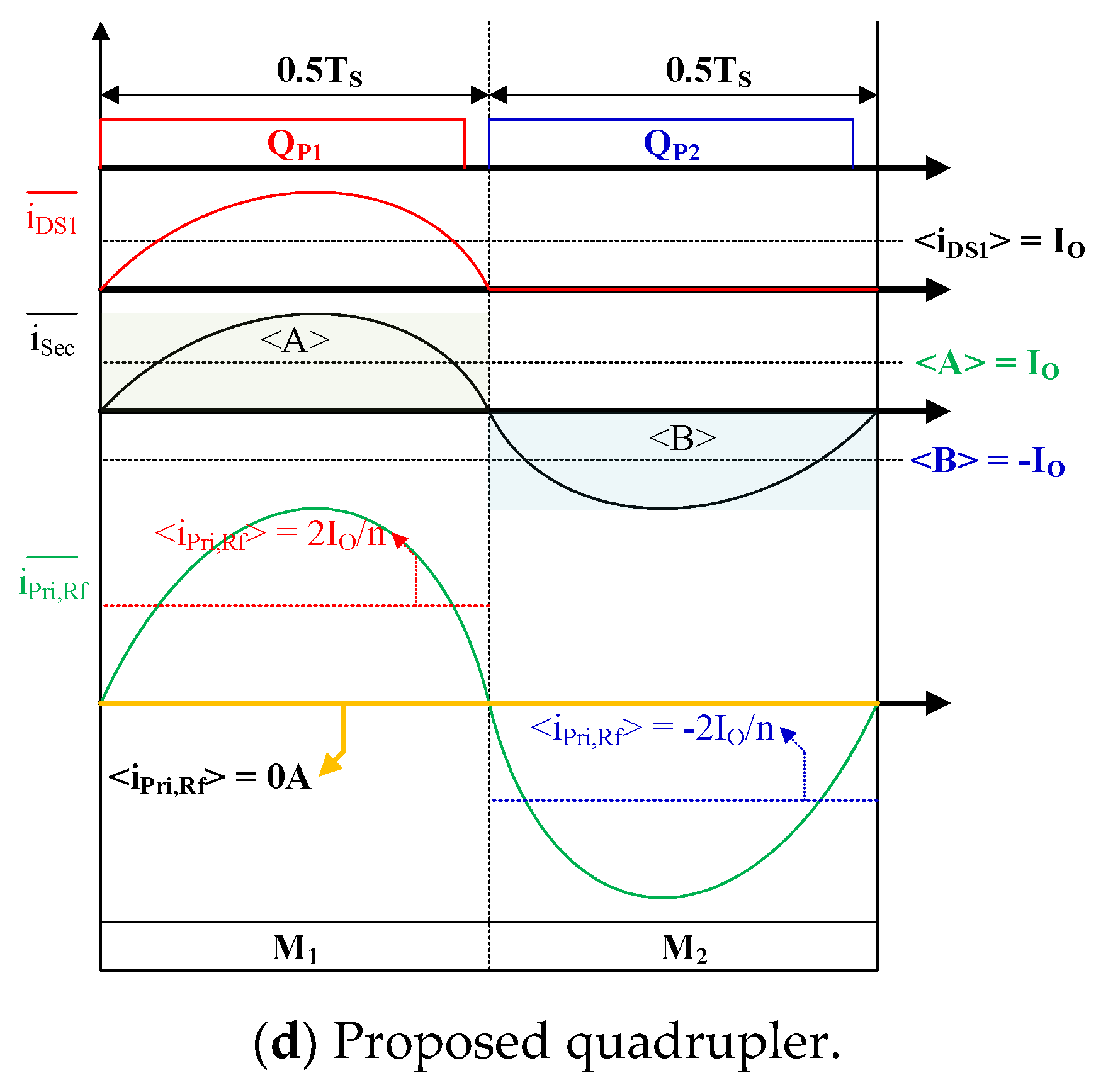
Fourth, in the proposed quadrupler rectifier, the secondary resonant current (i
Sec = i
DS1), which only flows in the secondary dot direction of N
S1 and N
S3, is transferred to the output through C
D and D
S1 during T
S/2, as shown in
Figure 2d, and its average should be the output current (I
O), as shown in
Figure 3d. Meanwhile, the secondary resonant current, flowing in the secondary undot direction of N
S1 and N
S2, does not pass through the output, but through C
D and D
S2, as shown in
Figure 2c. Due to the current-second balance on C
D, its average should be −I
O during the undot-direction operation. If the i
sec is reflected in the primary side of the transformer, each average of the reflected primary current (i
Pri,
Rf) is 2I
O/n or −2I
O/n during T
S/2, as shown in
Figure 3d. Due to the current-second balance on the primary resonant capacitor, the transformer magnetizing offset current is also zero in the proposed quadrupler rectifier.
2.2. Voltage and Current Stress on CD
As explained in
Section 2, in the VDR, and in the proposed tripler and quadrupler rectifiers, each voltage (V
D) on the secondary capacitor (C
D) is V
O/2, 2V
O/3, and V
O/2, respectively.
Meanwhile, in the VDR and the proposed tripler and quadrupler rectifiers, as explained in
Section 2.1, if the secondary resonant current only flows in the secondary dot direction, the secondary resonant current is transferred to the output during T
S/2. Assuming resonant operation, its average should be the output current (I
O), and the peak (i
Sec,
Pk) of the secondary resonant current can be obtained as πI
O from Equation (1), in the VDR and in the proposed tripler and quadrupler rectifiers. Since the secondary resonant current (i
Sec) flows through C
D, the current stress on C
D is πI
O.
Moreover, due to the current-second balance on CD, the secondary resonant current (iSec) can be expressed as πIO×sin(wt) during a period; thus, the rms current on CD is πIO/(2)0.5, in the VDR and in the proposed tripler and quadrupler rectifiers.
2.3. Voltage and Current Stress on DS1 and DS2
The voltage stress on a diode is determined when a diode is blocked.
In the CTR, if the secondary current (i
Sec) reflected from the primary flows in the secondary dot direction, D
S1 is conducted and D
S2 is blocked. Thus, the voltage across N
S1 is the output voltage (V
O), and the voltage stress on D
S2 is 2V
O by the secondary turns-ratio of the transformer, assuming N
S1 = N
S2. In the opposite situation, the voltage stress on D
S1 is 2V
O. Moreover, the secondary resonant current is twice transferred to the output during a period. Assuming resonant operation, its average should be the output current (I
O), and the peak (i
Sec,
Pk) of the secondary resonant current can be obtained as πI
O/2 from Equation (2).
Since the secondary resonant current (iSec) flows through DS1 or DS2, the current stress on DS1 and DS2 is πIO/2.
In the VDR, if the secondary current (iSec) reflected from the primary flows in the secondary dot direction, DS1 is conducted and DS2 is blocked. Thus, the voltage stress on DS2 is VO. On the other hand, if the secondary current (iSec) reflected from the primary flows in the secondary undot direction, DS2 is conducted and DS1 is blocked. Thus, the voltage stress on DS1 is VO.
In the proposed tripler rectifier, if the secondary current (iSec) reflected from the primary flows in the secondary dot direction, DS1 is conducted and DS2 is blocked. Since VD is 2VO/3, the voltage (VNS1) across NS1 is VO/3. Assuming NS1 = NS2, the voltage (VNS2) across NS2 is VO/3 in the dot direction; thus, the voltage stress on DS2 is 4VO/3. Meanwhile, if the secondary current (iSec) reflected from the primary flows in the secondary undot direction, DS2 is conducted and DS1 is blocked. Due to VD = 2VO/3, and assuming NS1 = NS2, the voltage (VNS2) across NS2 is VO/3 in the undot direction by the secondary turns-ratio of the transformer; thus, the voltage stress on DS1 is 2VO/3.
In the proposed quadrupler rectifier, if the secondary current (iSec) reflected from the primary flows in the secondary dot direction, DS1 is conducted and DS2 is blocked. Since VD is VO/2, the voltages (VNS1, VNS2, and VNS3) across NS1, NS2, and NS3 are VO/4 in the dot direction by the secondary turns-ratio of the transformer, assuming NS1 = NS2 = NS3. As a result, the voltages (VNS2 and VNS3) across NS2 and NS3 are cancelled, and the voltage stress on DS2 is VO. Meanwhile, if the secondary current (iSec) reflected from the primary flows in the secondary undot direction, DS2 is conducted and DS1 is blocked. Due to VD =VO/2, and assuming NS1 = NS2 = NS3, the voltages (VNS1, VNS2, and VNS3) across NS1, NS2, and NS3 are VO/4 in the undot direction by the secondary turns-ratio of the transformer. As a result, the voltages (VNS2 and VNS3) across NS2 and NS3 are cancelled, and the voltage stress on DS1 is VO.
On the other hand, in the VDR and in the proposed tripler and quadrupler rectifiers, due to once powering in a switching period, as explained in
Section 2.2, the average currents on D
S1 and D
S2 are I
O, and they are increased two times compared with that (I
O/2) in the CTR. Moreover, since the secondary resonant current (i
Sec) flows through D
S1 or D
S2, the current stresses on D
S1 or D
S2 are πI
O, which is equal to the current stress on C
D. Consequently, the multipliers have lower voltage stress and higher current stress than the CTR.
3. Design Guideline of Proposed Rectifiers
3.1. Design of Transformer Turns-Ratio
The I/O voltage gain (M = V
O/V
S) of the proposed voltage tripler is 3/(2n) at resonant frequency, as mentioned in
Section 2, Comparison and Analysis. Since “the input voltage (V
S) and output voltage (V
O) are, respectively, 400 V and 100 V” and “the highest efficiency is indicated at resonant frequency,” n is 6.
Meanwhile, the I/O voltage gain (M = V
O/V
S) of the proposed voltage quadrupler is 2/n at resonant frequency, as mentioned in
Section 2, Comparison and Analysis. Since “the input voltage (V
S) and output voltage (V
O) are, respectively, 400 V and 100 V” and “the highest efficiency is indicated at resonant frequency,” n is 8.
3.2. Design of Resonant Tanks (LR, CR, and LM)
The voltage gain (M = V
O/V
S) of the HB LLC converter can be expressed as follows [
7]:
where k = L
M/L
R, Q = (L
R/C
R)
0.5/R
O, f
R = 1/[2π(L
RC
R)
0.5], n = N
P/N
S, and f
S is the switching frequency.
Here, n’ indicates, respectively, 3/(2n) and 2/n in the proposed tripler and quadrupler rectifiers. Moreover, α indicates, respectively, 1/3 and 1/4 in the proposed tripler and quadrupler rectifiers. Assuming VS = 400 V and VO = 100 V, n should be 6 and 8 at resonant frequency in the proposed tripler and quadrupler rectifiers. In addition, since n′ and α × n are equal to 1/4 and 2 in both rectifiers, both voltage gains are the same.
Figure 4 shows equal voltage gain (M = V
O/V
S) in the proposed tripler and quadrupler rectifiers at full load condition, where I/O voltage gain is the lowest. Since Vs is 400 V and V
O is 100 V, the voltage gain (M) is 0.25. From
Figure 4, it is noted that M is 0.25 at resonant frequency (f
R = 80 kHz). By considering “double gain margin” and frequency variation range, L
M and L
R are designed at 500 μH and 62 μH, i.e., k = L
M/L
R ≈ 8. To operate at resonant frequency (f
R = 80 kHz) for high efficiency, C
R is designed at 62nF, i.e., f
R = 1/[2π(L
RC
R)
0.5] ≈ 80 kHz.
3.3. Design of Main Transformer
The core area (AC) is included in LM·iLM,Max = NP·BMax·AC, where iLM,Max is the maximum magnetizing inductor current, NP is the primary turns of the transformer, and BMax is the maximum flux density.
In the tripler rectifier, since the voltages (V
D and V
NS1) on C
D and secondary turns (N
S1) are 2V
O/3 and V
O/3 during 0.5 T
S of undot direction operation in
Figure 2a, the voltage (V
M) on the magnetizing inductor (L
M) is nV
O/3; thus, the ripple (∆i
LM) of the magnetizing inductor current is nV
O/(6·L
M·F
S). Meanwhile, the tripler rectifier has a transformer magnetizing offset current (i
LM,
Offset), i.e., i
LM,
Offset = I
O/n; thus, i
LM,
Max is the sum of i
LM,
Offset and ∆i
LM/2, i.e., i
LM,
Max = i
LM,
Offset (=I
O/n) + ∆i
LM/2[=nV
O/(12·L
M·F
S)]. Generally, the transformer turns-ratio (n) of the HB LLC resonant converter with the CTR is 2, but with the proposed tripler rectifier, it is is 6. As a result, the proposed tripler rectifier has a much smaller transformer magnetizing offset current, compared with [
1,
2,
3].
In the quadrupler rectifier, since the voltages (V
D and V
NS1) on C
D and secondary turns (N
S1) are V
O/2 and V
O/4 during 0.5 T
S of the undot direction operation, as shown in
Figure 2c, the voltage (V
M) on the magnetizing inductor (L
M) is nV
O/4; thus, i
LM,
Max is nV
O/(16·L
M·F
S).
On the other hand, the window area (AW) indicates the area to wind the primary and secondary windings. AW can be expressed as (NP·iLR,RMS + NS1·iNS1,RMS + NS2·iNS2,RMS)/(KU·J) in the tripler rectifier and (NP·iLR,RMS + NS1·iNS1,RMS + NS2·iNS2,RMS + NS3·iNS3,RMS)/(KU·J) in the quadrupler rectifier, where, respectively, iLR,RMS and iNSn,RMS mean the RMS current on the primary turns (NP) and the secondary turns (NSn) in the transformer, and KU and J mean the utilization factor of the window area and the current density of the primary and secondary wires in the transformer.
The turns-ratio (n) of the proposed tripler and quadrupler rectifiers were determined to be 6 and 8 by applying I/O voltage gain at resonant frequency. Moreover, LM was determined to be 500μH by considering “double gain margin” and frequency variation range. Assuming NP and AC are 48 and 170 mm2 because of VO = 100 V and FS = 80 kHz, the maximum flux density (BMax) is 0.097 T and 0.077 T, respectively, in the tripler and quadrupler rectifiers, which are within the saturation flux (BSat), i.e., BSat = 0.3 T. Due to iLM,Offset in the tripler rectifier, BMax in the tripler rectifier is higher. For high efficiency in high switching frequency, the variation (∆B) of the flux density, related to the core loss, is generally designed below 0.15 T. ∆B are equal to 0.153 T, because ∆iLM in both rectifiers are equal to 2.5 A. By considering ∆B and core volume (Ve), related to the core loss, the primary turns and core of the transformer are chosen at 48 turns and PQ3220 with “AC = 170 mm2 and PL-13 material.”
Meanwhile, in the tripler and quadrupler rectifiers, the peak (i
LR,
PK) of the primary current (i
LR) is πI
in, using a relationship that the average of the input current with i
LR and 0 A in half a cycle is equal to the input current (I
in); thus, the RMS (i
LR,
RMS) of i
LR is πI
in/2, i.e., i
LR,
RMS = 1.11 A. In the tripler and quadrupler rectifiers, the current (i
NS1) on N
S1 is equal to that on C
D from
Figure 2, and its RMS current (i
NS1,
RMS) is πI
O/2 from
Table 2, i.e., i
NS1,
RMS = 4.44 A. Moreover, in both rectifiers, the currents (i
NS2 and i
NS3) on N
S2 and N
S3 are the same as the half-cycle shape of the current on C
D from
Figure 2. As a result, their RMS currents (i
NS2,
RMS and i
NS3,
RMS) are all πI
O/2, i.e., i
NS2,
RMS = i
NS3,
RMS = 3.14 A. If K
U is 0.25 and J is 6 A/mm
2, A
W in the tripler and quadrupler rectifiers are, respectively, 76 mm
2 and 78.4 mm
2, which are suitable for PQ3220 with A
W = 80.8 mm
2.
Consequently, PQ3220 with PL-13 material, A
C = 170 mm
2, and A
W = 80.8 mm
2 was selected for the transformer in both rectifiers, by considering reasonable A
C and A
W as following
Table 4.
4. Experimental Results
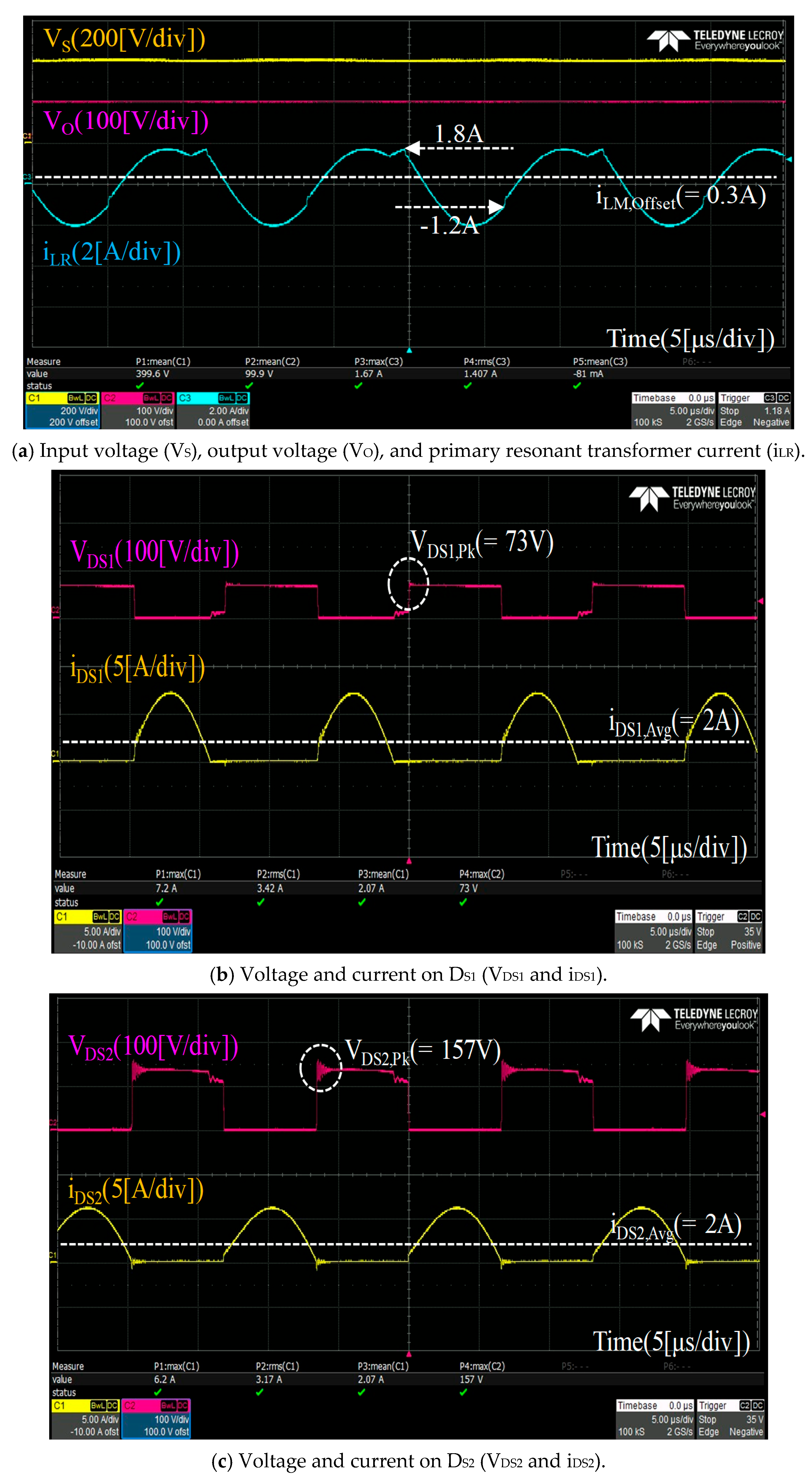
To verify the operation and analysis of the proposed rectifiers, the prototype was implemented using the half-bridge (HB) LLC resonant converter with the proposed voltage tripler and quadrupler rectifiers.
Table 5 and
Figure 5 show the experimental specifications, components, and circuits with used parameters of each component. The specifications are 400 V input and 100 V/200 W output. The transformer turns-ratios are 48:8:8, and 48:6:6:6 for the voltage tripler and quadrupler, respectively. From
Table 2, it is noted that the number of the secondary turns between the voltage tripler and quadrupler is three-fourths different, under the same primary turns.
Figure 6 and
Figure 7 show the experimental waveforms based on the realized H/W of the primary current (i
LR), and the voltages (V
DS1 and V
DS2) and currents (i
DS1 and i
DS2) of the secondary diodes in the voltage tripler and quadrupler, respectively.
The voltage tripler has asymmetric waveform in the primary current (i
LR), due to the magnetizing offset current about 0.33A (= I
O/n), as shown in
Figure 6a. This results from operations shown in
Figure 2a,b. During “undot direction like
Figure 2a” and “dot direction like
Figure 2b,” −2I
O/n and I
O/n are on average reflected to the primary side, respectively. In addition, “initial resonant currents” in i
LR are different at 1.8 A and −1.2 A, as shown in
Figure 6a, due to the magnetizing offset current. This results in “below or above operation” alternatively in a switching period. However, the primary current (i
LR) is symmetrical, due to there being no magnetizing offset current in the voltage quadrupler, as shown in
Figure 7a. This results from the operations, as shown in
Figure 2c,d. During “undot direction like
Figure 2c” and “dot direction like
Figure 2d,” −2I
O/n and 2I
O/n are on average reflected to the primary side, respectively. Therefore, i
LR in
Figure 6a and
Figure 7a has different shapes, due to the magnetizing offset current.
On the other hand, the average and peak values of the diode currents (i
DS1 and i
DS2) are about 2A (= I
O) and 6.3A (= πI
O), which are the same in the two rectifiers, as shown in
Figure 6b,c and
Figure 7b,c. The voltage stresses (V
DS1 and V
DS2) of D
S1 and D
S2 in the voltage tripler are 73 V (= 2V
O/3 [=67 V] + Ringing [=6 V]) and 157 V (= 4V
O/3 [=134 V] + Ringing [=23 V]), respectively, as shown in
Figure 6b,c. Those in the voltage quadrupler are 140 V (= V
O [=100 V] + Ringing [=40 V]) and 137 V (= V
O [=100 V] + Ringing [=37 V]), as shown in
Figure 7b,c. The difference in the voltage stresses on the secondary diodes results from the parasitic pattern leakage inductance.
Finally, the efficiencies of the voltage tripler and quadrupler are measured at about 94.1% and 93.7% at full load condition, respectively.
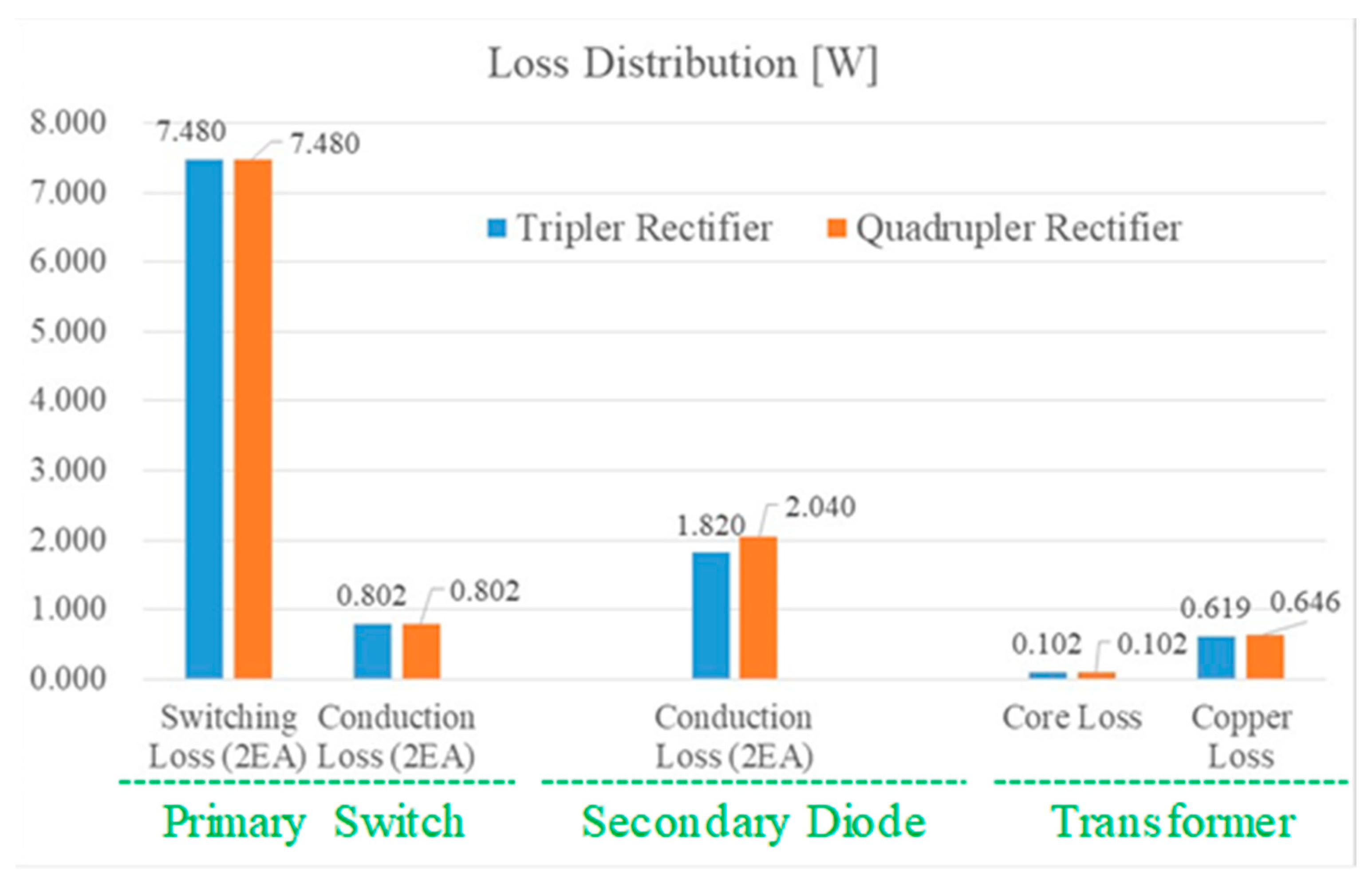
Figure 8 shows theoretical loss distribution in both voltage rectifiers. Both rectifiers use equal components “except for the secondary turns of the transformer and secondary diodes,” due to a very small magnetizing offset current (i
LM,
Offset = I
O/n) resulting from a large transformer turns-ratio (n), although the voltage tripler has i
LM,
Offset.
As shown in
Figure 8, the voltage tripler has less conduction loss on the secondary diodes (D
S1 and D
S2). This results from the small forward voltage of V20100C with a 100 V rating, compared with V20150C with a 150 V rating in the voltage quadrupler. Moreover, since the voltage tripler has fewer total secondary turns (16T) than those (18T) of the voltage quadrupler, it has slightly less copper loss in the transformer.
Consequently, the voltage tripler has slightly higher efficiency, due to the smaller conduction and copper losses in the secondary side than those of the voltage quadrupler; however, both rectifiers have almost equal efficiency.
5. Conclusions
New rectifiers are proposed in this paper. The proposed voltage tripler and quadrupler rectifiers have a simple structure with one capacitor and two diodes, and higher voltage gain with an equal turns-ratio or the same voltage gain with a larger turns-ratio. The proposed tripler and quadrupler rectifiers have several advantages, such as low component counts, a smaller transformer magnetizing offset current resulting from a larger turns-ratio, and no additional controls, compared with eight previous examples that can obtain additional I/O voltage gains in HB LLC resonant converters.
The rectifiers were compared and analyzed in respect of the transformer turns-ratio, the magnetizing offset current, and the voltage and current stresses of the secondary capacitor and diodes. Moreover, the design details, including the transformer turns-ratio, the resonant tanks, and the main transformer, which are different from those of conventional HB LLC resonant converters, were presented in this paper.
The validity of the basic operation and features was confirmed by the experiment using the half-bridge LLC resonant converter with 400 V input and 100 V/200 W output. Even though the diodes were adopted in the secondary side, the proposed tripler and quadrupler rectifiers achieved 94.1% and 93.7%, respectively. Moreover, the proposed tripler has the same size of transformer as the quadrupler rectifier, due to a much higher transformer turns-ratio, although it has a transformer magnetizing offset current.
This research will be helpful in applications requiring both high efficiency and a high step-up ratio in the half-bridge LLC resonant converter.


