
Review of Ka-Band Power Amplifier


Abstract
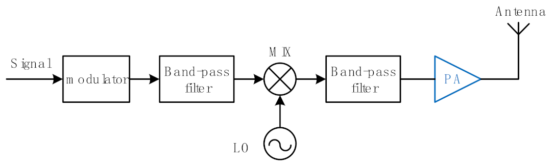
:1. Introduction
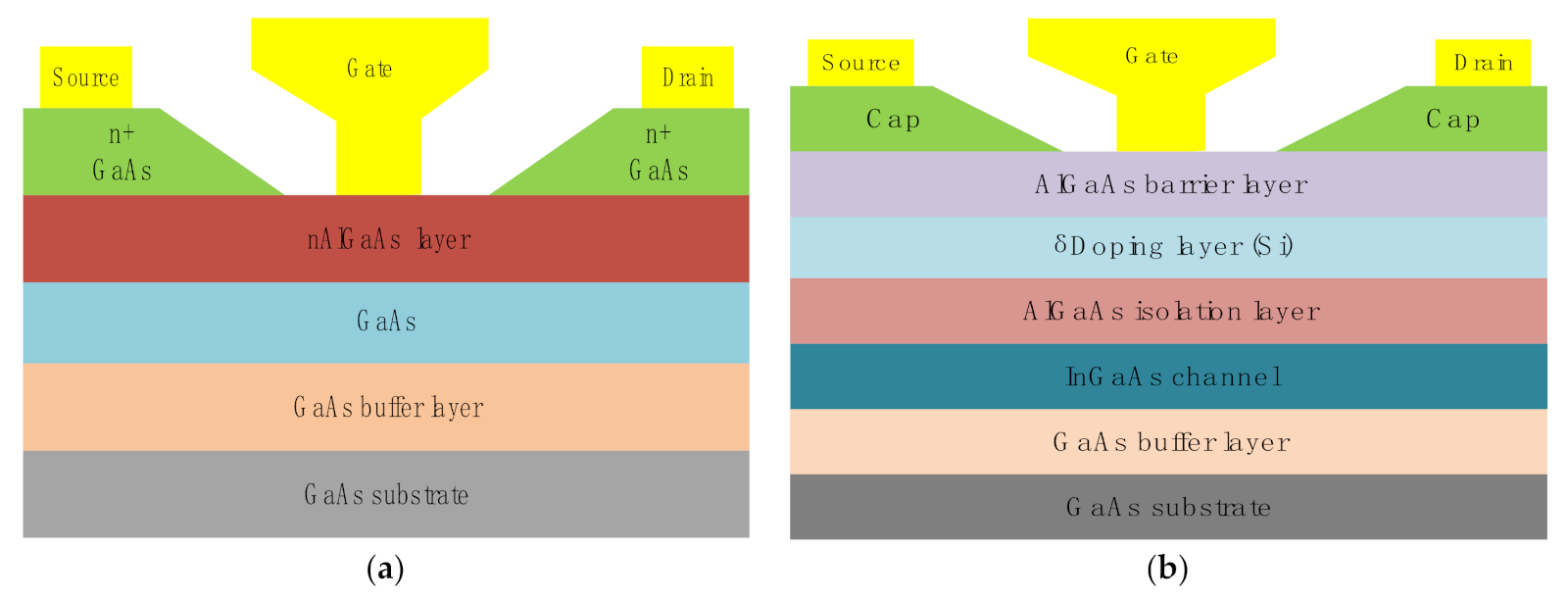
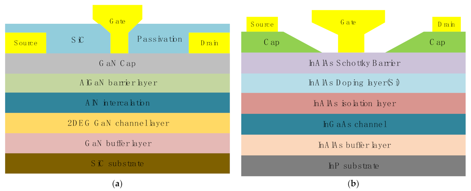
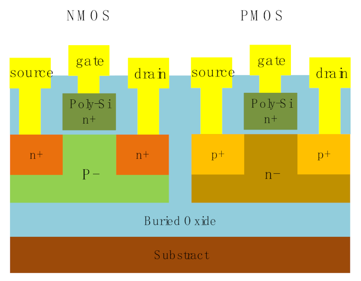
2. Technology
3. Topologies
3.1. Common Source
3.2. Cascode
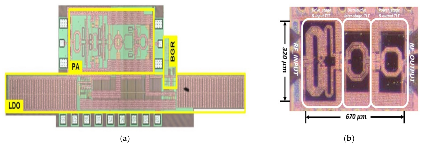
3.3. Stacked FET
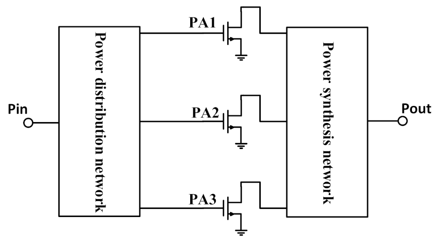
3.4. Power Combining
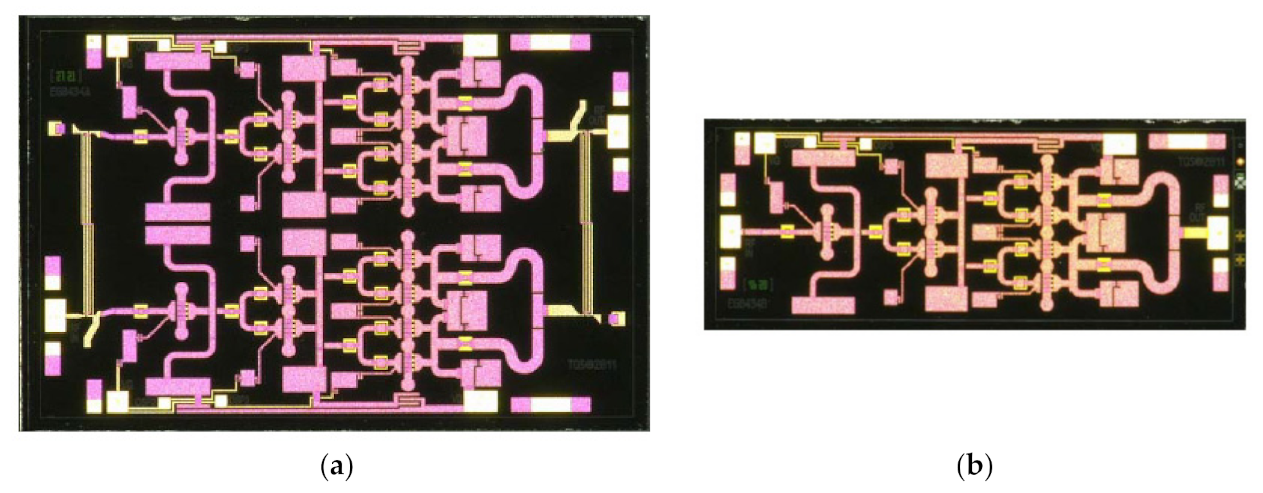
3.4.1. Corporate Combiner
3.4.2. Balanced Amplifier
3.4.3. Differential Amplifier
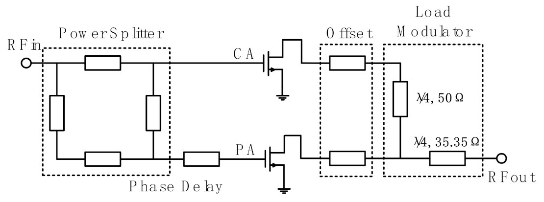
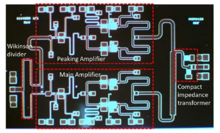
3.5. Doherty Power Amplifier
4. Conclusions
Author Contributions
Funding
Informed Consent Statement
Conflicts of Interest
References
- Xu, X.; Wang, N.; Wang, C. Reflection on the Development of Satellite Communications and the Integration with Terrestrial Mobile Communications. Aerosp. China 2021, 22, 59–66. [Google Scholar]
- Panagopoulos, A.D.; Arapoglou, P.; Cottis, P.G. Satellite communications at KU, KA, and V bands: Propagation impairments and mitigation techniques. Commun. Surv. Tutor. IEEE 2004, 6, 2–14. [Google Scholar] [CrossRef]
- Evans, J.V.; Proposed, U.S. Global satellite systems operating at Ka-Band. In Proceedings of the Aerospace Conference, Snowmass, CO, USA, 28–28 March 1998. [Google Scholar]
- Hasanuddin, Z.B.; Fujisaki, K.; Ishida, K.; Tateiba, M. Measurement of Ku-band rain attenuation using several VSATs in Kyushu Island, Japan. IEEE Antennas Wirel. Propag. Lett. 2002, 1, 116–119. [Google Scholar] [CrossRef]
- ViaSat-1 Led the Innovation of a New Class of Ka-Band Satellite Systems. Available online: http://www.viasat.com (accessed on 24 October 2021).
- High-Capacity Satellite System and ViaSat-1. Available online: https://www.viasat.com/space-innovation/satellite-fleet/viasat-1/ (accessed on 24 October 2021).
- ViaSat-1. Available online: http://www.ssloral.com (accessed on 24 October 2021).
- Deng, H.; Fei, P.; Yuan, J.; Shen, Y.; Pan, J. High Throughput Satellite System Capacity Analysis and Application Forecast. China Aerosp. 2016, 17, 30–40. [Google Scholar]
- Standard 3GPP Std.release 15; 3GPP 5G Mobile Broadband Standard Release 15. Available online: https://www.3gpp.org/release-15 (accessed on 26 October 2021).
- Sung, M.; Cho, S.-H.; Kim, J.; Lee, J.K.; Lee, J.H.; Chung, H.S. Demonstration of IFoF-Based Mobile Fronthaul in 5G Prototype With 28-GHz Millimeter wave. J. Lightwave Technol. 2018, 36, 601–609. [Google Scholar] [CrossRef]
- Gunnarsson, S.E.; Karnfelt, C.; Zirath, H.; Kozhuharov, R.; Kuylenstierna, D.; Alping, A.; Fager, C. Highly integrated 60 GHz transmitter and receiver MMICs in a GaAs pHEMT technology. IEEE J. Solid-State Circuits 2005, 40, 2174–2186. [Google Scholar] [CrossRef]
- Shinohara, K.; Regan, D.C.; Tang, Y.; Corrion, A.L.; Brown, D.F.; Wong, J.C.; Robinson, J.F.; Fung, H.H.; Schmitz, A.; Oh, T.C.; et al. Scaling of GaN HEMTs and Schottky Diodes for Submillimeter-Wave MMIC Applications. IEEE Trans. Electron Devices 2013, 60, 2982–2996. [Google Scholar] [CrossRef]
- Hamada, H.; Tsutsumi, T.; Matsuzaki, H.; Sugiyama, H.; Nosaka, H. 475-GHz 20-dB-Gain InP-HEMT Power Amplifier Using Neutralized Common-Source Architecture. In Proceedings of the 2020 IEEE/MTT-S International Microwave Symposium (IMS), Los Angeles, CA, USA, 4–6 August 2020. [Google Scholar]
- Iwai, H. Future of nano CMOS technology. Solid-State Electron. 2015, 112, 56–67. [Google Scholar] [CrossRef]
- Harame, D.L.; Ahlgren, D.C.; Coolbaugh, D.D.; Dunn, J.S.; Freeman, G.G.; Gillis, J.D.; Groves, R.A.; Hendersen, G.N.; Johnson, R.A.; Joseph, A.J.; et al. Current status and future trends of SiGe BiCMOS technology. IEEE Trans. Electron Device 2001, 48, 2575–2594. [Google Scholar] [CrossRef]
- Flandre, D.; Raskin, J.P.; Vanhoenacker-Janvier, D. Soi Cmos Transistors for RF and Microwave Applications. Int. J. High Speed Electron. Syst. 2001, 11, 1159–1248. [Google Scholar] [CrossRef]
- Yonezu, H.; Kobayashi, K.; Minemura, K.; Sakuma, I. GaAs-Al x Ga 1-x as double heterostructure laser for optical fiber communication system. In Proceedings of the 1973 International Electron Devices Meeting, Washington, DC, USA, 3–5 December 1973. [Google Scholar]
- Cho, A.; Casey, H. Molecular beam epitaxy: A technique for growth of GaAs-AlxGa1-xAs heterostructure lasers. IEEE J. Quantum Electron. 1974, 10, 791. [Google Scholar] [CrossRef]
- Lavanga, S.; Chini, A.; Coppa, A.; Corsaro, F.; Nanni, A.; Pantellini, A.; Romanini, P.; Lanzieri, C. High Voltage Breakdown pHEMTs for C-band HPA. In Proceedings of the Microwave Integrated Circuits Conference, Paris, France, 27–28 September 2010. [Google Scholar]
- Lang, D.V.; Logan, R.A.; Jaros, M. Trapping characteristics and a donor-complex (DX) model for the persistent-photoconductivity trapping center in Te-doped Al × Gal- ×As. Phys. Rev. B 1979, 19, 1015. [Google Scholar] [CrossRef]
- Ketterson, A.A.; Masselink, W.T.; Gedymin, J.S.; Klem, J.; Peng, C.-K.; Kopp, W.F.; Morkoc, F.; Gleason, K.R. Characterization of InGaAs/AlGaAs pseudomorphic modulation-doped field-effect transistors. IEEE Trans. Electron Devices 1986, 33, 564–571. [Google Scholar] [CrossRef]
- Li, X.J.; Ao, J.P.; Wang, R.; Liu, W.-J.; Wang, Z.-G.; Zeng, Q.-M.; Liu, S.-Y.; Liang, C.-G. An 850 nm wavelength monolithic integrated photoreceiver with a single-power-supplied transimpedance amplifier based on GaAs PHEMT technology. In Proceedings of the GaAs IC Symposium. IEEE Gallium Arsenide Integrated Circuit Symposium, 23rd Annual Technical Digest 2001 (Cat. No.01CH37191), Baltimore, MD, USA, 21–24 October 2001. [Google Scholar]
- Yung, Y.S. A tutorial on GaAs vs silicon. In Proceedings of the IEEE International Asic Conference & Exhibit, Rochester, NY, USA, 21–25 September 1992. [Google Scholar]
- Chien, F.-T.; Lin, D.-W.; Yang, C.-W.; Fu, J.S.; Chiu, H.-C. A low insertion loss GaAs pHEMT switch utilizing dual n+-doping AlAs etching stop layers design. Solid State Electron. 2010, 54, 231–234. [Google Scholar] [CrossRef]
- Barabi, A.; Ross, N.; Wolfman, A.; Shaham, O.; Socher, E. A +27 dbm psat 27 db gain w-band power amplifier in 0.1 μm gaas. In Proceedings of the 2018 IEEE/MTT-S International Microwave Symposium—IMS, Philadelphia, PA, USA, 10–15 June 2018. [Google Scholar]
- Elazar, T.; Socher, E. 95GHz 13dBm IQ-combined PA in 65nm CMOS. In Proceedings of the 2020 50th European Microwave Conference (EuMC), Utrecht, The Netherlands, 12–14 January 2021. [Google Scholar]
- Kumazaki, Y.; Ohki, T.; Kotani, J.; Ozaki, S.; Niida, Y.; Makiyama, K.; Minoura, Y.; Okamoto, N.; Nakamura, N.; Watanabe, K. Remarkable Current Collapse Suppression in GaN HEMTs on Free-standing GaN Substrates. In Proceedings of the 2019 IEEE BiCMOS and Compound semiconductor Integrated Circuits and Technology Symposium (BCICTS), Nashville, TN, USA, 3–6 November 2019. [Google Scholar]
- Shur, M.S. GaN based transistors for high power applications. Solid-State Electron. 1998, 42, 2131–2138. [Google Scholar] [CrossRef]
- Roberg, M.; Kywe, T.; Irvine, M.; Marrufo, O.; Nayak, S. 40 W Ka-Band Single and Dual Output GaN MMIC Power Amplifiers on SiC. In Proceedings of the IEEE BiCMOS and Compound Semiconductor Integrated Circuits and Technology Symposium, San Diego, CA, USA, 15–17 October 2018. [Google Scholar]
- Liao, M.; Shen, B.; Wang, Z. (Eds.) Ultra-Wide Bandgap Semiconductor Materials; Elsevier: Amsterdam, The Netherlands, 2019. [Google Scholar]
- Griffith, Z.; Urteaga, M.; Rowell, P. 180–265 GHz, 17–24 dBm output power broadband, high-gain power amplifiers in InP HBT. In Proceedings of the 2017 IEEE/MTT-S International Microwave Symposium—IMS, Honololu, HI, USA, 4–9 June 2017. [Google Scholar]
- Griffith, Z.; Urteaga, M.; Rowell, P. 190-260GHz High-Power, Broadband PA’s in 250nm InP HBT. In Proceedings of the Compound Semiconductor Integrated Circuit Symposium. IEEE, Honololu, HI, USA, 4–9 June 2017. [Google Scholar]
- Rizvi, A.; Jaiswal, P. Review on Present Trends in CMOS Scaling Technologies. Int. J. Sci. Eng. Technol. Res. 2016, 5, 953–956. [Google Scholar]
- Park, J.; Kang, S.; Hong, S. Design of a Ka-Band Cascode Power Amplifier Linearized with Cold-FET Interstage Matching Network. IEEE Trans. Microwave Theory Tech. 2021, 69, 1429–1438. [Google Scholar] [CrossRef]
- Adan, A.O.; Naka, T.; Kagisawa, A.; Shimizu, H. SOI as a mainstream IC technology. In Proceedings of the IEEE International Soi Conference, Stuart, FL, USA, 5–8 October 1998. [Google Scholar]
- Truyen, D.; Leduc, E.; Braud, F. Elimination of Single Event Latch-Up in the ATMEL ATMX150RHA Rad-Hard CMOS 150nm Cell-Based ASIC Family. In Proceedings of the 2015 15th European Conference on Radiation and Its Effects on Components and Systems (RADECS), Moscow, Russia, 14–18 September 2015. [Google Scholar]
- Udrea, F.; Popescu, A.; Milne, W. Breakdown analysis in JI, SOI and partial SOI power structures. In Proceedings of the IEEE International Soi Conference, Fish Camp, CA, USA, 6–9 October 1997. [Google Scholar]
- Sarkas, I.; Balteanu, A.; Dacquay, E.; Tomkins, A.; Voinigescu, S. A 45nm SOI CMOS Class-D mm-Wave PA with >10Vpp differential swing. In Proceedings of the Solid-state Circuits Conference Digest of Technical Papers, San Francisco, CA, USA, 19–23 February 2012. [Google Scholar]
- Bhat, R.; Chakrabarti, A.; Krishnaswamy, H. Large-scale power-combining and linearization in watt-class mmWave CMOS power amplifiers. In Proceedings of the Radio Frequency Integrated Circuits Symposium (RFIC), Seattle, WA, USA, 2–4 June 2013. [Google Scholar]
- Chakrabarti, A.; Krishnaswamy, H. High power, high efficiency stacked mmWave Class-E-like power amplifiers in 45nm SOI CMOS. In Proceedings of the Custom Integrated Circuits Conference (CICC), San Jose, CA, USA, 9–12 September 2012. [Google Scholar]
- Inac, O.; Uzunkol, M.; Rebeiz, G.M. 45-nm CMOS SOI Technology Characterization for Millimeter-Wave Applications. IEEE Trans. Microw. Theory Tech. 2014, 62, 1301–1311. [Google Scholar] [CrossRef]
- Lee, S.H.; Lee, J.Y.; Kim, S.H.; Bae, H.-C.; Lee, S.-Y.; Kang, J.-Y.; Kim, B.W. A 5.8 GHz MMIC Down-Conversion Mixer for DSRC Receiver using SiGe BiCMOS Process. In Proceedings of the 2005 Asia-Pacific Conference on Communications, Perth, WA, Australia, 5 October 2005. [Google Scholar]
- Pekarik, J.J.; Adkisson, J.; Gray, P.; Liu, Q.; Camillo-Castillo, R.; Khater, M.; Jain, V.; Zetterlund, B.; DiVergilio, A.; Tian, X.; et al. A 90nm SiGe BiCMOS technology for mm-wave and high-performance analog applications. In Proceedings of the Bipolar BiCMOS Circuites and Technology Meeting, Coronado, CA, USA, 28 September–1 October 2014. [Google Scholar]
- Pawlikiewicz, A.H.; Rai, S. RF CMOS or SiGE BiCMOS in RF and Mixed Signal Circuit Design. Mixed Design of Integrated Circuits and Systems, 2007. MIXDES ‘07. In Proceedings of the 14th International Conference on Mixed Design of Integrated Circuits and Systems, Ciechocinek, Poland, 21–23 June 2007. [Google Scholar]
- Lee, J.W.; Heo, S.M. A 27 GHz, 14 dBm CMOS Power Amplifier Using 0.18 Common-Source MOSFETs. IEEE Microw. Wirel. Compon. Lett. 2008, 18, 755–757. [Google Scholar] [CrossRef]
- Ali, S.N.; Agarwal, P.; Renaud, L.; Molavi, R.; Mirabbasi, S.; Pande, P.P.; Heo, D. A 40% PAE Frequency-Reconfigurable CMOS Power Amplifier with Tunable Gate–Drain Neutralization for 28-GHz 5G Radios. IEEE Trans. Microw. Theory Tech. 2018, 66, 2231–2245. [Google Scholar] [CrossRef]
- Chang, Y.-T.; Hung, L.-C.; Lu, H.-C. A 28 GHz Power Amplifier Combing Linearizer, Adaptive Bias and Gm Compensation to Improve Back-off and P1dB Efficiency. In Proceedings of the 2020 50th European Microwave Conference (EuMC), Utrecht, The Netherlands, 12–14 January 2021. [Google Scholar]
- Komijani, A.; Hajimiri, A. A 24GHz, +14.5dBm fully-integrated power amplifier in 0.18 um CMOS. In Proceedings of the IEEE 2004 Custom Integrated Circuits Conference (IEEE Cat. No.04CH37571), Orlando, FL, USA, 6 October 2004. [Google Scholar]
- Jeong, D.; Moon, K.; Lee, S.; Park, B.; Kim, J.; Son, J.; Kim, B. Linear CMOS power amplifier at Ka-band with ultra-wide video bandwidth. In Proceedings of the 2017 IEEE Radio Frequency Integrated Circuits Symposium (RFIC), Honolulu, HI, USA, 4–6 June 2017. [Google Scholar]
- Kim, B.; Park, B.; Jin, S. Design of an Advanced CMOS Power Amplifier. J. Electromagn. Eng. Sci. 2015, 15, 63–75. [Google Scholar] [CrossRef] [Green Version]
- Jin, S.; Kwon, M.; Moon, K.; Park, B.; Kim, B. Control of IMD Asymmetry of CMOS Power Amplifier for Broadband Operation Using Wideband Signal. IEEE Trans. Microw. Theory Tech. 2013, 61, 3753–3762. [Google Scholar] [CrossRef]
- Shuo-Hsuan, C.; Chun-Nien, C.; Huei, W. A Ka-Band Dual-Mode Power Amplifier in 65-nm CMOS Technology. IEEE Microw. Wirel. Compon. Lett. 2018, 28, 1–3. [Google Scholar]
- Aikio, J.P.; Rahkonen, T. A comprehensive analysis of AM-AM and AM-PM conversion in an LDMOS RF power amplifier. IEEE Trans. Microw. Theory Tech. 2009, 57, 262–270. [Google Scholar] [CrossRef]
- Cho, G.; Jeong, G.; Hong, S. 28-GHz CMOS Power Amplifier Linearized with Resistive Drain-Body Connection. IEEE Microw. Wirel. Compon. Lett. 2020, 30, 876–879. [Google Scholar] [CrossRef]
- Boroujeni, S.R.; Basaligheh, A.; Ituah, S.; Nezhad-Ahmadi, M.-R.; Safavi-Naeini, S. A Broadband High-Efficiency Continuous Class-AB Power Amplifier for Millimeter-Wave 5G and SATCOM Phased-Array Transmitters. IEEE Trans. Microw. Theory Tech. 2020, 68, 3159–3171. [Google Scholar] [CrossRef]
- Zhang, S.; Madic, J.; Bretchko, P.; Mokoro, J.; Shumovich, R.; McMorrow, R. A novel power-amplifier module for quad-band wireless handset applications. IEEE Trans. Microw. Theory Tech. 2003, 51, 2203–2210. [Google Scholar] [CrossRef]
- Huynh, C.; Nguyen, C. New Technique for Synthesizing Concurrent Dual-Band Impedance-Matching Filtering Networks and 0.18um SiGe BiCMOS 25.5/37-GHz Concurrent Dual-Band Power Amplifier. IEEE Trans. Microw. Theory Tech. 2013, 61, 3927–3939. [Google Scholar] [CrossRef]
- Fritsche, D.; Wolf, R.; Ellinger, F. Analysis and Design of a Stacked Power Amplifier with Very High Bandwidth. IEEE Trans. Microw. Theory Tech. 2012, 60, 3223–3231. [Google Scholar] [CrossRef]
- Park, B.; Jeong., D.; Kim, J.; Cho, Y.; Moon, K.; Kim, B. Highly linear CMOS power amplifier for mm-wave applications. In Proceedings of the 2016 IEEE MTT-S International Microwave Symposium (IMS), San Francisco, CA, USA, 22–27 May 2016. [Google Scholar]
- Nguyen, D.P.; Pham, A.V. An Ultra Compact Watt-Level Ka-Band Stacked-FET Power Amplifier. IEEE Microw. Wirel. Compon. Lett. 2016, 26, 516–518. [Google Scholar] [CrossRef] [Green Version]
- Lee, Y.C.; Chen, T.Y.; Liu, Y.C. An adaptively biased stacked power amplifier without output matching network in 90-nm CMOS. In Proceedings of the 2017 IEEE/MTT-S International Microwave Symposium—IMS 2017, Honololu, HI, USA, 4–9 June 2017. [Google Scholar]
- Zhou, Q.; Li, Z.; Cheng, G.; He, W.; Wang, H. A 26.5-40GHz SiGe Stacked Cascode Power Amplifier. In Proceedings of the 2018 14th IEEE International Conference on Solid-State and Integrated Circuit Technology (ICSICT), Qingdao, China, 31 October–3 November 2018. [Google Scholar]
- Chang, Y.; Lu, B.-Z.; Wang, Y.; Wang, H. A Ka-Band Stacked Power Amplifier with 24.8-dBm Output Power and 24.3% PAE in 65-nm CMOS Technology. In Proceedings of the 2019 IEEE MTT-S International Microwave Symposium (IMS), Boston, MA, USA, 2–7 June 2019. [Google Scholar]
- Ali, S.; Hasan, S. A 38-GHz Millimeter-Wave Double-Stacked HBT Class-F1 High-Gain Power Amplifier in 130-nm SiGe-BiCMOS. IEEE Trans. Microw. Theory Tech. 2020, 68, 3039–3044. [Google Scholar] [CrossRef]
- Wang, H.; Tsai, J.-H.; Lin, K.Y.; Tsai, Z.-M.; Huang, T.-W. MM-Wave Integration and Combinations. IEEE Microw. Mag. 2012, 13, 49–57. [Google Scholar] [CrossRef]
- Aust, M.V.; Sharma, A.K.; Fordham, O.; Grundbacher, R.; To, R.; Tsai, R.; Lai, R. A highly efficient Q-band MMIC 2.8 Watt output power amplifier based on 0.15μm InGaAs/GaAs pHEMT process technology. In Proceedings of the IEEE Compound Semiconductor Integrated Circuit Symposium, Palm Springs, CA, USA, 30 October–2 November 2005. [Google Scholar]
- Mi, C.; Zhu, X.; Meng, F.; Zhang, N. A Highly Efficient Combined Power Amplifier with Branch-line Couplers. In Proceedings of the 2018 IEEE Wireless Power Transfer Conference (WPTC), Montreal, QC, Canada, 3–7 June 2018. [Google Scholar]
- Jiang, Y.S.; Tsai, J.H.; Wang, H. A W-Band Medium Power Amplifier in 90 nm CMOS. IEEE Microw. Wirel. Compon. Lett. 2008, 18, 818–820. [Google Scholar] [CrossRef]
- Tirado-Mendez, A.; Jardon-Aguilar, H.; Flores-Leal, R.; Andrade-Gonzalez, E.; Reyes-Ayala, M. Low-harmonic distortion in single-ended and push-pull class E power amplifier by using slotted microstrip lines. AEU Int. J. Electron. Commun. 2010, 64, 66–74. [Google Scholar] [CrossRef]
- Lin, S.; Fathy, A.; Hegazi, G.M.; Chu, T.T. Multi—octave high power recycling combiner using coaxial line to improve overall efficiency of outphasing power amplifier. In Proceedings of the 2008 IEEE Radio and Wireless Symposium, Orlando, FL, USA, 22–24 January 2008; pp. 747–750. [Google Scholar]
- Komijani, A.; Natarajan, A.; Hajimiri, A. A 24-GHz, +14.5-dBm fully integrated power amplifier in 0.18-/spl mu/m CMOS. IEEE J. Solid-State Circuits 2005, 40, 1901–1908. [Google Scholar] [CrossRef]
- Danzillio, D. Advanced GaAs Integration for Single Chip mmWave Front-Ends. Microw. J. 2018, 61, 148–156. [Google Scholar]
- Kim, B.; Tserng, H.Q.; Shih, H.D. 44-GHz monolithic GaAs FET amplifier. IEEE Electron Device Lett. 1986, 7, 95–97. [Google Scholar] [CrossRef]
- Matsunaga, K.; Miura, I.; Iwata, N. A CW 4-W Ka-Band Power Amplifier Utilizing MMIC Multichip Technology. IEEE J. Solid-State Circuits 2000, 35, 1293–1297. [Google Scholar] [CrossRef]
- Campbell, C.F.; Dumka, D.C.; Kao, M.Y.; Fanning, D.M. High Efficiency Ka-Band Power Amplifier MMIC Utilizing a High Voltage Dual Field Plate GaAs PHEMT Process. In Proceedings of the 2011 IEEE Compound Semiconductor Integrated Circuit Symposium (CSICS), Waikoloa, HI, USA, 16–19 October 2011; pp. 1–4. [Google Scholar]
- Noh, Y.S.; Yom, I.B. A Linear GaN High Power Amplifier MMIC for Ka-Band Satellite Communications. IEEE Microw. Wirel. Compon. Lett. 2016, 26, 619–621. [Google Scholar] [CrossRef]
- Gasmi, A.; El Kaamouchi, M.; Poulain, J.; Wroblewski, B.; Lecourt, F.; Dagher, G.; Frijlink, P.; Leblanc, R. 10W power amplifier and 3W transmit/receive module with 3 dB NF in Ka band using a 100nm GaN/Si process. In Proceedings of the 2017 IEEE Compound Semiconductor Integrated Circuit Symposium (CSICS), Miami, FL, USA, 22–25 October 2017; pp. 1–4. [Google Scholar]
- Neininger, P.; John, L.; Bruckner, P.; Friesicke, C.; Quay, R.; Zwick, T. Design, Analysis and Evaluation of a Broadband High-Power Amplifier for Ka-Band Frequencies. In Proceedings of the 2019 IEEE MTT-S International Microwave Symposium (IMS), Boston, MA, USA, 2–7 June 2019; pp. 564–567. [Google Scholar]
- Neininger, P.; John, L.; Thome, F.; Friesicke, C.; Brückner, P.; Quay, R.; Zwick, T. Limitations and Implementation Strategies of Interstage Matching in a 6-W, 28-38-GHz GaN Power Amplifier MMIC. IEEE Trans. Microw. Theory Tech. 2021, 69, 2541–2553. [Google Scholar] [CrossRef]
- Chéron, J.; Campovecchio, M.; Quéré, R.; Schwantuschke, D.; Quay, R.; Ambacher, O. High-efficiency power amplifier MMICs in 100 nm GaN technology at Ka-band frequencies. In Proceedings of the 2013 European Microwave Integrated Circuit Conference, Nuremberg, Germany, 6–8 October 2013; pp. 492–495. [Google Scholar]
- Estella, N.; Camargo, E.; Schellenberg, J.; Bui, L. High-Efficiency, Ka-band GaN Power Amplifiers. In Proceedings of the 2019 IEEE MTT-S International Microwave Symposium (IMS), Boston, MA, USA, 2–7 June 2019; pp. 568–571. [Google Scholar]
- Hosseinzadeh, N.; Medi, A. Wideband 5 W Ka-Band GaAs Power Amplifier. IEEE Microw. Wirel. Compon. Lett. 2016, 26, 622–624. [Google Scholar] [CrossRef]
- Ingram, D.L.; Stones, E.I.; Elliott, J.H.; Wang, H.; Lai, R.; Biedenbender, M. A 6-W Ka-band power module using MMIC power amplifiers. IEEE Trans. Microw. Theory Tech. 1997, 45, 2424–2430. [Google Scholar] [CrossRef]
- Siddiqui, M.K.; Sharma, A.K.; Callejo, L.G.; Lai, R. A high-power and high-efficiency monolithic power amplifier at 28 GHz for LMDS applications. IEEE Trans. Microw. Theory Tech. 1998, 46, 2226–2232. [Google Scholar] [CrossRef]
- Kinayman, N.; Jenkins, A.; Helms, D.; Gresham, I. Design of 24 GHz SiGe HBT balanced power amplifier for system-on-a-chip ultra-wideband applications. In Proceedings of the 2005 IEEE Radio Frequency integrated Circuits (RFIC) Symposium-Digest of Papers, Long Beach, CA, USA, 12–14 June 2005; pp. 91–94. [Google Scholar]
- Campbell, C.F.; Kao, M.-Y.; Nayak, S. High efficiency Ka-band power amplifier MMICs fabricated with a 0.15µm GaN on SiC HEMT process. In Proceedings of the 2012 IEEE/MTT-S International Microwave Symposium Digest, Montreal, QC, Canada, 17–22 June 2012; pp. 1–3. [Google Scholar]
- Chen, S.; Nayak, S.; Campbell, C.; Reese, E. High Efficiency 5W/10W 32–38GHz Power Amplifier MMICs Utilizing Advanced 0.15m GaN HEMT Technology. In Proceedings of the 2016 IEEE Compound Semiconductor Integrated Circuit Symposium (CSICS), Austin, TX, USA, 23–26 October 2016; pp. 1–4. [Google Scholar]
- Jia, H.; Prawoto, C.C.; Chi, B.; Wang, Z.; Yue, C.P. A Full Ka-Band Power Amplifier with 32.9% PAE and 15.3-dBm Power in 65-nm CMOS. IEEE Trans. Circuits Syst. I Regul. Pap. 2018, 65, 2657–2668. [Google Scholar] [CrossRef]
- Chiang, K.-C.; Tsai, T.-C.; Huang, I.; Tsai, J.-H.; Huang, T.-W. A 27-GHz Transformer Based Power Amplifier with 513.8-mW/mm 2 Output Power Density and 40.7% Peak PAE in 1-V 28-nm CMOS. In Proceedings of the 2019 IEEE MTT-S International Microwave Symposium (IMS), Boston, MA, USA, 2–7 June 2019; pp. 1283–1286. [Google Scholar]
- Huang, W.C.; Wang, H. An Inductive-Neutralized 26-dBm K-/Kₐ-Band Power Amplifier with 34% PAE in 90-nm CMOS. IEEE Trans. Microw. Theory Tech. 2019, 99, 1–14. [Google Scholar]
- Chou, C.; Hsiao, Y.H.; Wu, Y.C.; Lin, Y.-H. Design of a V-Band 20-dBm Wideband Power Amplifier Using Transformer-Based Radial Power Combining in 90-nm CMOS. IEEE Trans. Microw. Theory Tech. 2016, 64, 1–16. [Google Scholar] [CrossRef]
- Lin, Y.T.; Chen, C.N.; Lin, J.L.; Wang, H. A 38 GHz Pre-Distortion Power Amplifier with OP 1dB and IM 3 Improvement in 65-nm CMOS Process. In Proceedings of the 2019 IEEE Asia-Pacific Microwave Conference (APMC), Singapore, 10–13 December 2019. [Google Scholar]
- Wang, F.; Li, T.W.; Wang, H. 4.8 A Highly Linear Super-Resolution Mixed-Signal Doherty Power Amplifier for High-Efficiency mm-Wave 5G Multi-Gb/s Communications. In Proceedings of the 2019 IEEE International Solid-State Circuits Conference—(ISSCC), San Francisco, CA, USA, 17–21 February 2019. [Google Scholar]
- Qunaj, V.; Reynaert, P. 26.2 A Doherty-Like Load-Modulated Balanced Power Amplifier Achieving 15.5dBm Average P out and 20% Average PAE at a Data Rate of 18Gb/s in 28nm CMOS. In Proceedings of the 2021 IEEE International Solid-State Circuits Conference (ISSCC), San Francisco, CA, USA, 13–22 February 2021. [Google Scholar]
- Curtis, J.; Pham, A.V.; Chirala, M. A Ka-Band doherty power amplifier with 25.1 dBm output power, 38% peak PAE and 27% back-off PAE. Radio Frequency Integrated Circuits Symposium (RFIC). In Proceedings of the 2013 IEEE Radio Frequency Integrated Circuits Symposium (RFIC), Seattle, WA, USA, 2–4 June 2014. [Google Scholar]
- Nguyen, D.P.; Pham, T.; Pham, A.V. A Ka-band asymmetrical stacked-FET MMIC Doherty power amplifier. In Proceedings of the Radio Frequency Integrated Circuits Symposium. IEEE Trans. Microwave Theory Tech. 2017, 66, 227–236. [Google Scholar] [CrossRef]
- Nguyen, D.P.; Curtis, J.; Pham, A.V. A Doherty Amplifier with Modified Load Modulation Scheme Based on Load-Pull Data. IEEE Trans. Microw. Theory Tech. 2017, 66, 1–10. [Google Scholar] [CrossRef]
- Indirayanti, P.; Reynaert, P. A 32 GHz 20 dBm-PSAT transformer-based Doherty power amplifier for multi-Gb/s 5G applications in 28 nm bulk CMOS. In Proceedings of the Radio Frequency Integrated Circuits Symposium, Honolulu, HI, USA, 4–6 June 2017; pp. 45–48. [Google Scholar]
- Chen, Y.-C.; Lin, Y.-H.; Lin, J.-L.; Wang, H. AKa-Band Transformer-Based Doherty Power Amplifier for Multi-Gb/s Application in 90-nm CMOS. IEEE Microw. Wirel. Compon. Lett. 2018, 28, 4430–4452. [Google Scholar] [CrossRef]
- Tsai, J.H.; Huang, T.W. A 38–46 GHz MMIC Doherty Power Amplifier Using Post-Distortion Linearization. IEEE Microw. Wirel. Compon. Lett. 2007, 17, 388–390. [Google Scholar] [CrossRef]
- Chen, Y.; Chen, C.N.; Chiong, C.C.; Wang, H. A Compact 40-GHz Doherty Power Amplifier with 21% PAE at 6-dB Power Back Off in 0.1-. IEEE Microw. Wirel. Compon. Lett. 2019, 29, 545–547. [Google Scholar] [CrossRef]
- Nguyen, D.P.; Pham, B.L.; Pham, A.V. A compact 29% PAE at 6 dB power back-off E-mode GaAs pHEMT MMIC Doherty power amplifier at Ka-band. In Proceedings of the 2017 IEEE MTT-S International Microwave Symposium (IMS), Honololu, HI, USA, 4– 9 June 2017. [Google Scholar]
- Chen, W.; Lv, G.; Xin, L.; Feng, Z. Energy-efficient doherty power amplifier MMIC and beamforming-oriented digital predistortion for 5G massive MIMO application. In Proceedings of the IEEE Asia Pacific Microwave Conference, Kuala Lumpur, Malaysia, 13–16 November 2017. [Google Scholar]
- Lin, Y.A.; Ji, J.R.; Chien, T.H.; Chang, T.-Z.; Wang, Y.-C. A Ka-band 25-dBm output power high efficiency monolithic Doherty power amplifier in 0.15-μm GaAs E-mode pHEMT process. In Proceedings of the 2017 IEEE Asia Pacific Microwave Conference, Kuala Lumpur, Malaysia, 13–16 November 2017. [Google Scholar]
- Rostomyan, N.; Ozen, M.; Asbeck, P. 28 GHz Doherty Power Amplifier in CMOS SOI with 28% Back-Off PAE. IEEE Microw. Wirel. Compon. Lett. 2018, 28, 446–448. [Google Scholar] [CrossRef]
- Wang, F.; Wang, H. 24.1 A 24-to-30GHz Watt-Level Broadband Linear Doherty Power Amplifier with Multi-Primary Distributed-Active-Transformer Power-Combining Supporting 5G NR FR2 64-QAM with >19dBm Average Pout and >19% Average PAE. In Proceedings of the 2020 IEEE International Solid- State Circuits Conference—(ISSCC), San Francisco, CA, USA, 16–20 February 2020. [Google Scholar]


| Ref. | Tech | Frequency (GHz) | Gain (dB) | (dBm) | (dBm) | (%) | Area (mm2) | Topology |
|---|---|---|---|---|---|---|---|---|
| [45] | 180 nm CMOS | 24 | 14.5 | 14 | / | 13.2 | 0.84 | 3-stage CS |
| [46] | 65 nm CMOS | 24/28 | 9.1/8.1 | 14.7/14.4 | 13.9/13.6 | 42.6/40.1 | 0.11 | 1-stage CS |
| [47] | 90 nm CMOS | 28 | 21.3 | 17.7 | 16.7 | 23.6 | 0.49 | 3-stage CS |
| Ref. | Tech | Frequency (GHz) | Gain (dB) | (dBm) | (dBm) | (%) | Area (mm2) | Topology |
|---|---|---|---|---|---|---|---|---|
| [48] | 180 nm CMOS | 24 | 7 | 14.5 | / | / | 1.26 | 2-stage cascode |
| [49] | 65 nm CMOS | 28 | 22 | 14 | / | 21.8 | 0.53 | 3-stage CS cascode |
| [52] | 65 nm CMOS | 34 | 13.8/10.5 | 19.9/17 | 17/14 | 25.8/22.8 | 0.365 | 2-stage cascode |
| [54] | 40 nm CMOS | 28 | 20.1 | 20.3 | 18.3 | 25 | 0.214 | 2-stage Differential cascode |
| [55] | 130 nm SiGe | 28 | / | 14 | 12 | 25 | 0.14 | 1-stage cascode |
| [34] | 65 nmCMOS | 31 | 18.9 | 20.3 | / | 38.2 | 0.345 | 2-stage cascode |
| [57] | 180 nm SiGe BiCMOS | 25.5/37 | 20.5 | 14.6 | 13.1 | 35.8 | 0.3 | 2-stage CE cascode |
| Ref | Tech | Frequency (GHz) | Gain (dB) | (dBm) | (dBm) | (%) | Area (mm2) | Topology |
|---|---|---|---|---|---|---|---|---|
| [59] | 28 nm CMOS | 28 | 10/13.6 | 10.1/15.1 | 14/18.6 | 36.5/43.3 | 0.28# | 1-Stage CS differential /2-stage stacked |
| [60] | 150 nm GaAs | 26–31 | 16.7 | 31.5 | / | 33 | 2.08 | 3-stage stacked |
| [61] | 90 nm CMOS | 32 | 17.2 | 17.6 | 13.2 | 25.3 | 0.3 # | 3-stage stacked |
| [62] | 180 nm SiGe BiCMOS | 26.5–40 | 20.1 | 25.3 | 23.6 | 31.7 | 1.26 | cascode stacked |
| [63] | 65 nm CMOS | 38 | 17.5 | 24.8 | 21.7 | 24.3 | 0.146 # | 3-stage stacked |
| [64] | 130 nm SiGe BiCMOS | 38 | 22.1 | 21.2 | 17.5 | 30.1 | 0.75 * | 2-stage Class-F−1 stacked |
| Ref. | Tech | Frequency (GHz) | Gain (dB) | (dBm) | (dBm) | (%) | Area (mm2) | Topology |
|---|---|---|---|---|---|---|---|---|
| [74] | 350 nm GaAs | 26.5–28.5 | / | 34.8 | / | / | 84.0 | 4-MMICs parallel combined |
| [75] | 150 nm GaAs | 35 | 23 | 37.2 | / | 30 | 14.7 | 3-stage combined |
| [76] | 150 nm GaN | 28 | 10.6 | 39.9 | / | 35 | 8.5 | 3-stage combined |
| [77] | 100 nm GaN/Si | 29–33 | 25 | 40 | / | 30 | 15.75 | 3-stage combined |
| [78] | 100 nm GaN/SiC | 26–33 | 22 | 38 | / | 25 | 15.8 | 3-stage combined |
| [79] | 150 nm GaN/SiC | 28–39 | 15 | 38.2 | / | 26.1 | 14.0 | 3-stage reactive combined |
| [80] | 100 nm GaN/SiC | 29 | 14 | 36.7 | / | 28 | 9.0 | 2-stage combined |
| [81] | 200 nm GaN | 31.5 | 25 | 40 | / | 36 | 16.7 | 2-stage combined |
| [82] | 100 nm GaN | 31–40 | 20 | 37 | 35 | 28.2 | 11.9 | Combined with IBVW |
| [83] | 150 nm GaAs | 33 | 11.5 | 35.4 | / | 28 | 6 | 2-stage MMIC balanced |
| [84] | 150 nm GaAs | 28 | 16 | 32 | / | 35 | / | 2-stage balanced |
| [85] | SiGe | 24 | 18 | 12 | / | / | / | 3-stage CE balanced |
| [86] | 150 nm GaN | 28.5/29 | 24/25 | 39.4/37 | / | 26/30 | 9.7/4.8 | 2-stage/4-stage balanced |
| [87] | 150 nm GaN | 38 | 13 | 37.1 | / | 33 | 9.9 | Two 3-stage balanced combined |
| [88] | 65 nm CMOS | 32 | 20.8 | 15.3 | 12.9 | 32.6 | 0.11 # | 2-stage CS differential |
| [89] | 28 nm CMOS | 27 | 13.1 | 17.9 | 14.7 | 40.7 | 0.12 | 1-stage CS differential |
| [90] | 90 nm CMOS | 28 | 16.3 | 26 | 23.2 | 34.1 | 0.401 | 2-stage cascode differential |
| [92] | 65 nmCMOS | 38 | 19.7 | 16.8 | 14.2 | 33.6 | 0.31 | 2-stage CS differential |
| Ref. | Tech | Frequency (GHz) | Gain (dB) | (dBm) | PBO † (%) | (%) | Area (mm2) | Topology |
|---|---|---|---|---|---|---|---|---|
| [95] | 150 nm GaAs | 26.4 | 10.3 | 25.3 | 27 | 38 | 25 | Doherty PA |
| [96] | 150 nm GaAs | 25.5–29.5 | 15 | / | 27 | 37 | 4.93 | Doherty PA |
| [97] | 150 nm GaAs | 28.5–31.5 | 10.5 | / | 32 | 38 | 4.59 | Doherty PA |
| [98] | 28 nm CMOS | 32 | 6.7 | 19.8 | / | 21 | 1.87 | Doherty PA |
| [99] | 90 nm CMOS | 28.7–41.9 | 19.8 | 20.7 | 13.1 | 32.7 | 0.203 * | Doherty PA |
| [100] | 150 nm GaAs | 38–46 | 7 | 21.8 | 17 | / | 2 | Doherty PA |
| [103] | 150 nm GaAs | 29–31.8 | / | 25.7–26.8 | 21–32 †† | 31–38 | 3.57 | Doherty PA |
| [104] | 150 nm GaAs | 25.8 | 7 | 25.1 | 12.6 | 16.5 | 2.25 | Doherty PA |
| [105] | 45 nm SOI CMOS | 28 | 10 | 22.4 | 28 | 40 | 0.63 * | Doherty PA |
| [106] | 130 nm SiGeBiCMOS | 28 | 20.5 | 28.3 | 27.8 | 30.4 | 4.19 | Doherty PA |
Publisher’s Note: MDPI stays neutral with regard to jurisdictional claims in published maps and institutional affiliations. |
© 2022 by the authors. Licensee MDPI, Basel, Switzerland. This article is an open access article distributed under the terms and conditions of the Creative Commons Attribution (CC BY) license (https://creativecommons.org/licenses/by/4.0/).
Share and Cite
Wang, Z.; Hu, S.; Gu, L.; Lin, L. Review of Ka-Band Power Amplifier. Electronics 2022, 11, 942. https://doi.org/10.3390/electronics11060942
Wang Z, Hu S, Gu L, Lin L. Review of Ka-Band Power Amplifier. Electronics. 2022; 11(6):942. https://doi.org/10.3390/electronics11060942
Chicago/Turabian StyleWang, Zhong, Shanwen Hu, Ling Gu, and Lujun Lin. 2022. "Review of Ka-Band Power Amplifier" Electronics 11, no. 6: 942. https://doi.org/10.3390/electronics11060942