Article

A Novel Single-Stage Common-Ground Transformerless Buck–Boost Inverter

1
Department of Electrical Engineering, Chonnam National University, Gwangju 61186, Korea
2
Faculty of Electrical and Electronics Engineering, Ho Chi Minh City University of Technology and Education, Ho Chi Minh City 700000, Vietnam
3
Faculty of Electrical Engineering Technology, Industrial University of Ho Chi Minh City, Ho Chi Minh City 700000, Vietnam
*
Authors to whom correspondence should be addressed.
Electronics 2022, 11(5), 829; https://doi.org/10.3390/electronics11050829
Submission received: 28 January 2022 / Revised: 2 March 2022 / Accepted: 4 March 2022 / Published: 7 March 2022
(This article belongs to the Special Issue Innovative Technologies in Power Converters)

Abstract

:
In this article, a novel single-stage transformerless buck–boost inverter is introduced. The proposed inverter can share a common ground between the DC input side and the grid; this leads to having a zero-leakage current. The proposed inverter also provides the buck and boost voltage capabilities. Additionally, the power switches are operated at high frequency in the half-cycle of the sinusoidal wave, so the efficiency of the proposed inverter can be improved. Operating analysis, design consideration, comparison, and simulation study are presented. Finally, a 500 W laboratory prototype is also built to confirm the correctness and feasibility of the proposed inverter.

1. Introduction

In recent years, the nearly exhausted fossil fuels and environmental deterioration have promoted the development of renewable energy sources such as wind power, photovoltaic (PV), fuel cells, and ocean waves [1,2,3,4]. Among these renewable energy sources, the PV market has several advantages, which include being inexhaustible, as well as its easy availability and pollution-free operation. Moreover, the main technological evolution for the PV system is the inverter. The inverter can be divided into two types with transformer topologies [5,6,7] or transformerless topologies [8,9,10]. Although transformer-based inverters can provide galvanic isolation and protection, they have undesirable properties such as high cost and weight, with additional losses [9,10]. On the other hand, transformerless inverters have reduced costs and sizes, and improved efficiency, but the isolation between the PV panel and the inverter system leads to the occurrence of leakage current. This leakage current causes a rise in harmonic distortion, in both output voltage and current, which also results in electromagnetic interference between the PV system and grid. To eliminate leakage current, the DC current injection from the inverter should also be reduced, as presented in the standards IEEE 1547 and IEC 61727 [11,12]. Moreover, the transformerless inverter topologies can be classified into two groups—namely, two-stage configurations and single-stage configurations. In two-stage configurations, the power processing is divided into two stages. A DC–DC boost converter is added between the inverter side and DC input power supply side, which boosts a low-voltage input to the high voltage required for the second stage [13,14,15]. The next stage is an inverter that converts DC voltage to AC voltage to connect with the grid. Two-stage transformerless inverter topologies can have some disadvantages, including low efficiency, increased cost, and complexity control in a two-stage configuration. In contrast, single-stage configurations have all the functions of boosting ability and maximum power extraction, as well as DC–AC conversion. Compared with two-stage configurations, single-stage configurations have more benefits, including compactness, lower device count, lower costs, and greater efficiency [16]. From this point of view, single-stage inverters are reported in the literature, and their comprehensive review is given in [17,18,19,20,21,22,23,24,25,26,27]. Common-ground transformerless inverter topologies were introduced in [21,22,23,24,25,28,29,30], which directly connect the ground of the grid to the negative of the DC input source. The common-mode voltage is equal to zero, and it also protects against any high-frequency content. Therefore, there is no common-mode leakage current in the presented topologies.
In order to improve the boosting capability and provide common ground with single-stage configuration, single-stage, common-ground transformerless inverters have been used in [23] without a continuous input current. However, the power switches are operated at high frequency. This leads to an increase in the switching loss of the inverter. Similarly, a buck–boost inverter in [24] with five switches is proposed to achieve the common-ground condition and wide buck–boost voltage operation. However, three switches are operated at a high switching frequency in the half-line period. The single-phase transformerless grid-connected PV inverter introduced in [25,26] also focuses on a doubly grounded inverter with single-stage conversion and uses fewer components. Nevertheless, the disadvantage of this inverter is also the high switching frequency of its power switches. To further improve the voltage gain, a novel step-up transformerless inverter is presented in [27]. This inverter can provide the common ground between the output and input sides with a single stage. However, it requires more switches, which increases the size and cost of the inverter package.
In this article, a novel single-stage common-ground transformerless buck–boost inverter (CGBBI) is proposed to eliminate leakage current elimination and achieve voltage boosting capability. Moreover, the PWM control method of the proposed inverter can reduce the high switching loss on semiconductor devices. The remainder of this article is organized as follows: First, the inverter configuration, PWM control method, and operating principle of the proposed inverter are presented in Section 2. Design guidelines of the devices are given in Section 3. A comparative study is provided in Section 4, drawing on other existing common-ground buck–boost inverter topologies. Simulation and experimental results are presented in Section 5 to evaluate the accurate performance of the proposed inverter. Finally, the conclusions of the study are drawn in Section 6.

2. Derivation of Proposed CGBBI

The proposed CGBBI topology is shown in Figure 1. The major characteristic of the proposed CGBBI topology is to have a common point between the output side and the negative terminal of the input DC power supply, which avoids the leakage current [9]. The proposed CGBBI topology includes five power switches S1S5, three diodes D1D3, two inductors L1L2, two capacitors C1C2, and one output filter inductor Lf. It can be seen that the proposed CGBBI topology is composed of one buck–boost module, one boost module, and one power switch operating at low frequency. The buck–boost module comprises three power switches S1S3, two diodes D1D2, and a pair of L1 and C1. Similarly, the boost module has one power switch S4, one diode D3, one inductor L2, and one capacitor C2.

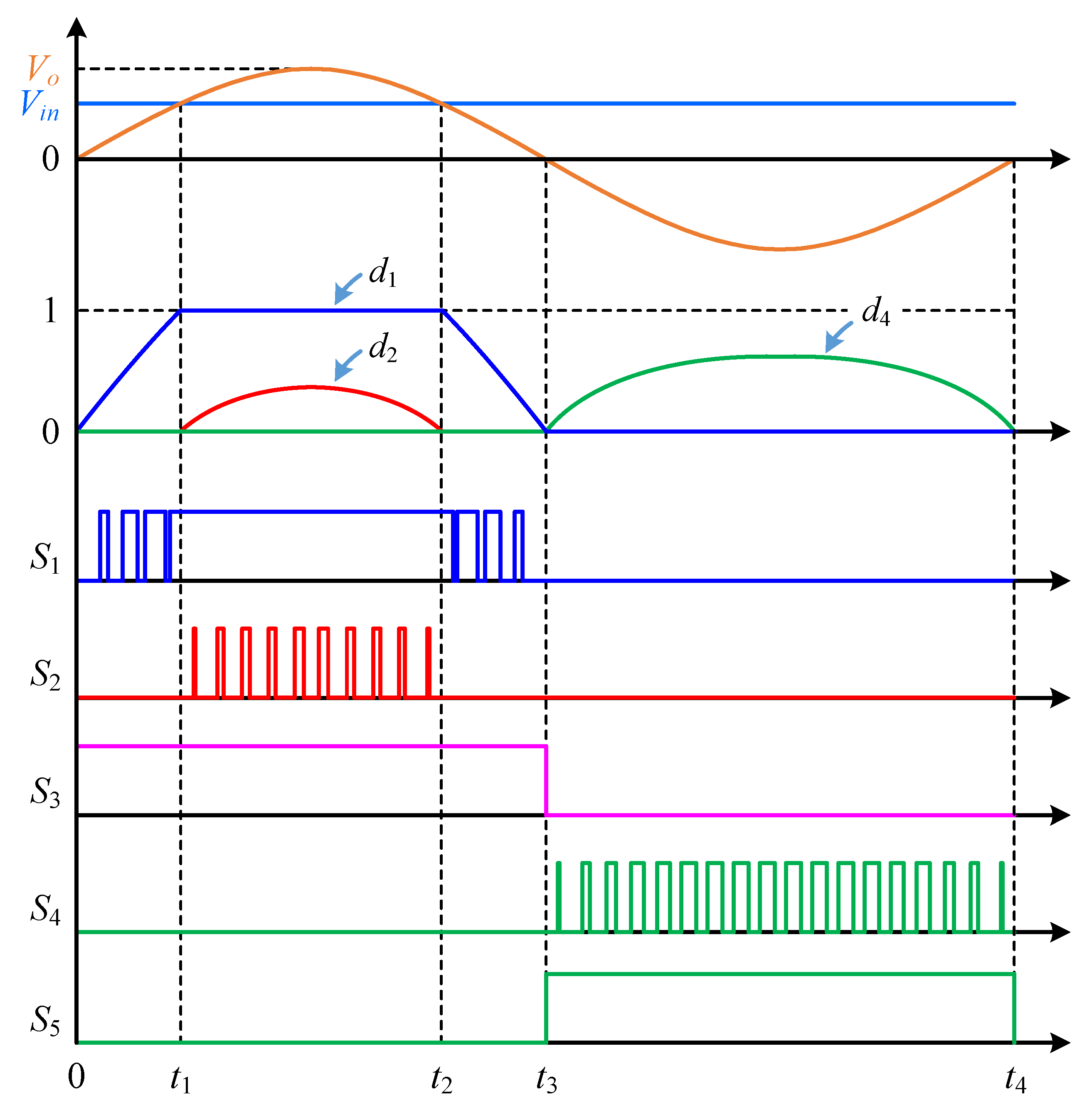
2.1. PWM Control Method for the Proposed CGBBI Topology

Figure 2 presents the PWM control method for the proposed CGBBI topology. When output voltage vo is higher than 0, switch S3 is turned on, and S4 and S5 are turned off. However, switches S1 and S2 are turned on/off alternately at high frequency. When the output voltage vo is negative, three switches S1, S2, and S3 are turned off, while S5 is turned on. In this case, only switch S4 is operated at high frequency during this negative half-line cycle.

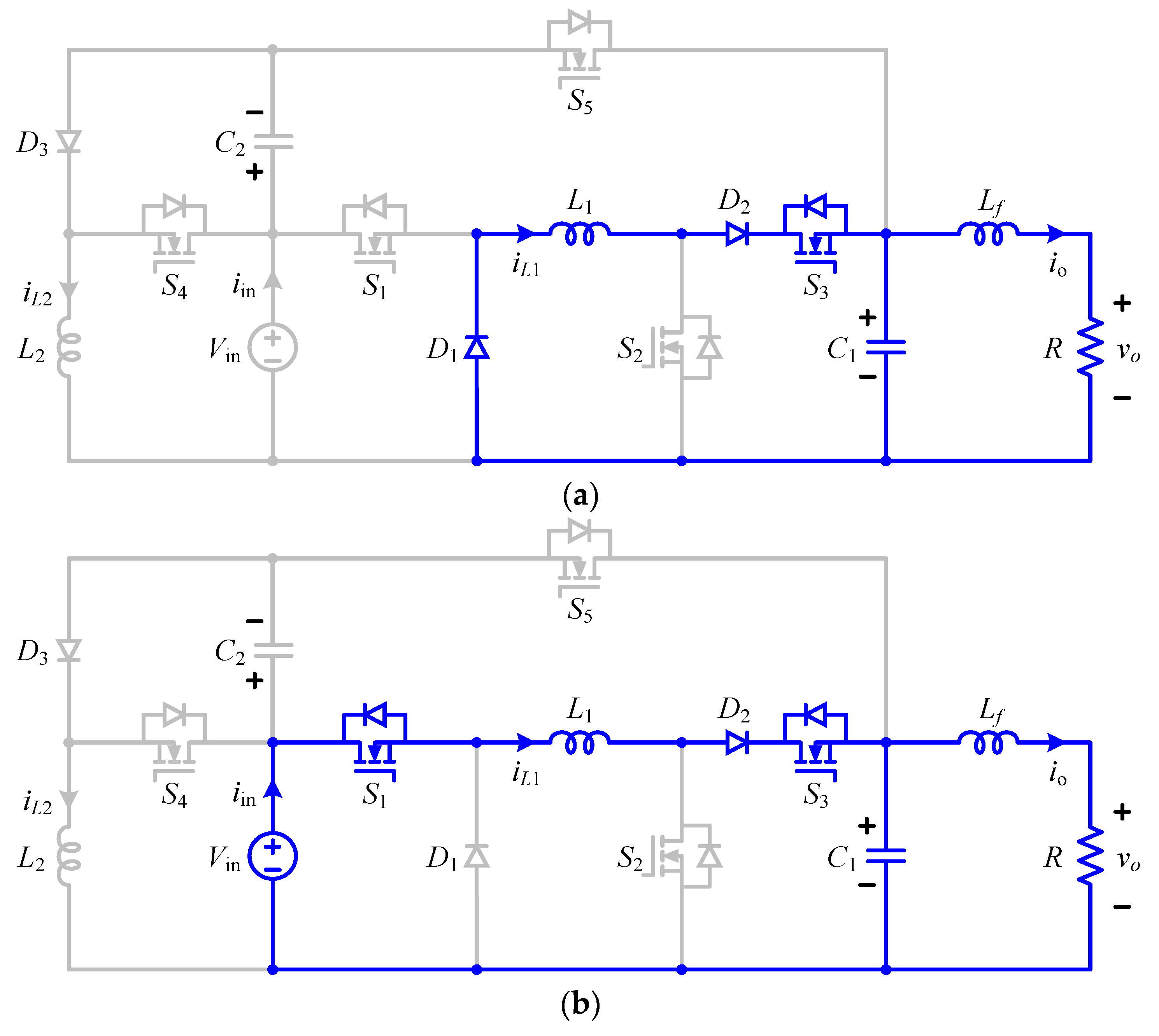
2.2. Operating of the Proposed CGBBI Topology

Interval 1 ([0, t1] or [t2, t3]): This interval appears when the voltage Vin is higher than vo. In this case, only the buck–boost module is operated. Switch S3 is turned on, while S2, S4, and S5 are turned off. It can be seen that only switch S1 is turned on and off at high frequency. Voltage vC1 is equal to vo. In terms of the inductor current, iL1 approximates the output current, while iL2 is zero.
Mode 1 (Figure 3a): Switch S1 is turned off, and diodes D1D2 are forward biased. Inductor L1 is connected to the capacitor C1 and load, to which it charges energy. In this mode, capacitor C1 provides energy to the load and maintains the constant output voltage across the load. We have
{ L 1 d i L 1 d t = v o C 1 d v C 1 d t = i L 1 i o
Mode 2 (Figure 3b): Switch S1 is turned on, diode D1 is reverse biased and D2 is forward biased. Inductor L1 is charged by an input voltage Vin, capacitor C1, and the load. The inductor current iL1 increases linearly. The equations in this mode can be derived as follows:
{ L 1 d i L 1 d t = V i n v o C 1 d v C 1 d t = i L 1 i o
By applying voltage-second balance condition to an inductor L1, the relationship between vo and Vin can be obtained as
v o = d 1 V i n
where d1 is the duty ratio of S1.
Interval 2 ([t1, t2]): This interval appears when the input voltage Vin is lower than vo. In this case, only the buck–boost module operates. Switch S1 is turned on, while S4 and S5 are kept off. Only switch S2 is turned on and off at high frequency. Voltage vC1 is equal to vo, while inductor current iL1 is larger than output current, and inductor current iL2 is zero.
Mode 1 (Figure 4a): Switch S2 in the buck–boost converter is turned on. Consequently, diodes D1 and D2 are reverse biasED. The voltage in inductor L1 equals the input voltage Vin. Inductor current iL1 increases linearly, and capacitor C1 charges the load. The related equations are as follows:
{ L 1 d i L 1 d t = V i n C 1 d v C 1 d t = i o
Mode 2 (Figure 4b): Switch S2 is turned off, diode D1 is reverse biased, and D2 is forward biased. The power supply and inductor L1 charge energy to filter the capacitor and the load, so capacitor C1 is charged, and inductor current iL1 decreases linearly. We have
{ L 1 d i L 1 d t = V i n v o C 1 d v C 1 d t = i L 1 i o
The relationship between vo and Vin can be obtained from (4) and (5).
v o = V i n 1 d 2
where d2 is the duty ratio of S2.
Interval 3 ([t3, t4]): The output voltage is negative, and it can be observed that only the boost module operates in this interval. Switch S5 is turned on and switches S1, S2, and S3 are turned off. In this case, only switch S4 is controlled at high frequency. Voltage vC1 is equal to output voltage vo. Capacitor voltage vC2 is the total voltage of input voltage and output voltage, while inductor current iL1 is equal to 0, and inductor current iL2 is higher than the output current.
Mode 1 (Figure 5a): Switch S4 is turned on, and diode D3 is reverse biased in this mode. Inductor L2 is charged from the input voltage, and the inductor current iL2 increases linearly. The capacitor C2 transfers power to the load. The equations of this mode can be found as follows:
{ L 2 d i L 2 d t = V i n C 2 d v C 2 d t = i i n i L 2 C 1 d v C 1 d t = i i n i L 2 i o
Mode 2 (Figure 5b): Switch S4 is turned off, and diode D3 is forward biased. Inductor L2 transfers energy to capacitor C2 through diode D3. In this mode, the energy of inductor L2 is also transferred to capacitor C1 and the load through S5 and D3, so the inductor current iL2 decreases linearly. We have
{ L 2 d i L 2 d t = V i n v C 2 C 2 d v C 2 d t = i i n C 1 d v C 1 d t = i i n i o i L 2
From (7) and (8), we have
v o = d 4 V i n d 4 1
where d4 is the duty ratio of S4.
When vo > 0, the voltage in capacitors C1 and C2 can be given as
{ v C 1 = V o s i n ω t v C 2 = V i n
When vo < 0, the voltage in capacitors C1 and C2 can be rewritten as
{ v C 1 = V o s i n ω t v C 2 = V i n V o s i n ω t
where Vo is the peak value of output voltage, and ω is the angular frequency.
The relationship between the input voltage and the peak value of output voltage can be determined as follows:
M = V o V i n
where M is the modulation index.
The resulting duty cycles for the PWM modulation are visualized in Figure 2 and are calculated based on (12).
From (3), (6), (9), (12), the corresponding duty cycles for the PWM control method are defined in (13) and (14) as follows:
{ d 1 ( t ) = M s i n ω t d 2 ( t ) = 1 1 M s i n ω t d 4 ( t ) = 0 ,   w h e n   v o > 0
{ d 1 ( t ) = 0 d 2 ( t ) = 0   d 4 ( t ) = M s i n ω t M s i n ω t 1 ,   w h e n   v o < 0
According to (13) and (14), the maximum values of the corresponding duty cycles can be expressed as
{ D 1 . m a x = M D 2 . m a x = 1 1 M   w i t h   M > 1 D 2 . m a x = 0   w i t h   M 1 D 4 . m a x = M M + 1
In order to determine the switching state in the PWM control method, shown in Figure 2, interval 2 is executed when the output voltage is higher than the input voltage. The values of t1 and t2 are calculated as follows:
{ t 1 = 1 ω s i n 1 ( 1 M ) t 2 = π 1 ω s i n 1 ( 1 M )

3. Parameter Design

3.1. Selection of the Inductors

Using (1), (2), (4), (5), (7), and (8), applying the volt-second balance principle on L1 and L2, the inductors L1 and L2 currents can be calculated using (17) and (18).
i L 1 = { I o s i n ω t ,   0 < t t 1   a n d   t 2 < t t 3 I o s i n ω t 1 d 2 ,   t 1 < t t 2 0 ,   t 3 < t t 4
i L 2 = { 0 ,   0 < t t 3 I o s i n ω t d 4 1 ,   t 3 < t t 4
where Io is the peak value of output current.
According to (17), (18), and (12), the peak value of inductors L1 and L2 currents can be given by (19) and (20).
I L 1 = { I o ,   M 1 M I o ,   M > 1
I L 2 = ( M + 1 ) I o
The inductors can be designed by using the equation of their current ripple, using (17), (18), and (15), while the peak-to-peak current ripple of inductors L1 and L2 can be defined by (21) and (22).
Δ i L 1 . m a x = { V i n 4 f s L 1 ,   M 1 ( M 1 ) V i n M f s L 1 ,   M > 1
Δ i L 2 . m a x = M V i n ( M + 1 ) f s L 2
where fs denotes the switching frequency.
According to (19)–(22), the inductance values of L1 and L2 can be calculated using (23) and (24) as follows:
L 1 = { V i n 4 f s x % I o ,   M 1 ( M 1 ) V i n M 2 f s x % I o ,   M > 1
L 2 = M V i n ( M + 1 ) 2 f s x % I o
where x% is the inductors L1 and L2 ripple.
Based on the maximum value of the current through the inductors L1, L2 in (19) and (20). The stored energy of the inductor is given by
W m = 1 2 L I L . m a x 2
The required area product of the inductor, as cited in [31,32], is
A p = 2 W m K u B m J m
where Ku, Bm, and Jm are the core window of the fill factor, the amplitude of a magnetic flux density in the core, and the amplitude in current density of the winding conductor, respectively.

3.2. Selection of the Capacitors

Using the equations given in (15), the peak-to-peak voltage ripple of capacitors C1 and C2 can be defined as
Δ v C 1 . m a x = { V i n 32 L 1 C 1 f s 2 ,   M 1 ( M 1 ) I o M f s C 1 ,   M > 1
Δ v C 2 . m a x = M I o ( M + 1 ) f s ( C 1 + C 2 )
According to (27) and (28), the capacitance values of C1 and C2 are calculated as follows:
C 1 = { V i n 32 y L 1 f s 2 ,   M 1 ( M 1 ) I o M f s y % V o ,   M > 1
C 2 = M I o ( M + 1 ) f s y % V o C 1
where y% is the capacitors C1 and C2 ripple.

3.3. Selection of Switching Devices

The voltage stress across the switches and the diodes are given in (31)–(34).
{ V D S 1 = V D 1 = V i n V D S 2 = V D S 3 = V D S 5 = V D 2 = V o   V D S 4 = V D 3 = V i n + V o
The current stresses of switches S1S5 reach the maximum when the output current has its peak value (Io), as given by (32)–(34).
{ I S 1 = I S 3 = I D 1 = I D 2 = I L 1 = I o I S 2 = 0 ,   M 1
{ I S 1 = I S 2 = I S 3 = I D 2 = I L 1 = M I o I D 1 = I o s i n ω t 1   ,   M > 1
I S 5 I S 4 = I D 3 = I L 2 = ( M + 1 ) I o

3.4. Power Loss Calculation

3.4.1. Power Loss of Power Switches

The total power loss of the switches is equal to the sum of the conduction losses and switching losses, given by
P S _ t o t = P S _ c o n + P S _ s w
P S _ c o n = i = 1 5 R d s i I S i . r m s 2
P S _ s w = i = 1 5 V S i I S i . a v g ( t r i + t f i ) f s
where Rdsi, tri, and tfi are the on-state drain-source resistance, the turn-on and turn-off delay times of each MOSFET, respectively.
The average and RMS current values through the switches are calculated as
{ I S 1 . a v g = 1 2 π [ 2 0 t 1 i L 1 ( t ) d 1 ( t ) d ( ω t ) + t 1 t 2 i L 1 ( t ) d ( ω t ) ] I S 1 . r m s = 1 2 π [ 2 0 t 1 i L 1 2 ( t ) d 1 ( t ) d ( ω t ) + t 1 t 2 i L 1 2 ( t ) d ( ω t ) ]  
{ I S 2 . a v g = 1 2 π [ t 1 t 2 i L 1 ( t ) d 2 ( t ) d ( ω t ) ] I S 2 . r m s = 1 2 π [ t 1 t 2 i L 1 2 ( t ) d 2 ( t ) d ( ω t ) ]
{ I S 3 . a v g = 1 2 π [ t 1 t 2 i L 1 ( t ) [ 1 d 2 ( t ) ] d ( ω t ) ] I S 3 . r m s = 1 2 π [ t 1 t 2 i L 1 2 ( t ) [ 1 d 2 ( t ) ] d ( ω t ) ]  
{ I S 4 . a v g = 1 2 π [ π 2 π i L 2 ( t ) d 4 ( t ) d ( ω t ) ] I S 4 . r m s = 1 2 π [ π 2 π i L 2 2 ( t ) d 4 ( t ) d ( ω t ) ]  
{ I S 5 . a v g = 1 2 π [ π 2 π [ i L 2 ( t ) I i n ] [ 1 d 4 ( t ) ] d ( ω t ) ] I S 5 . r m s = 1 2 π [ π 2 π [ i L 2 ( t ) I i n ] 2 [ 1 d 4 ( t ) ] d ( ω t ) ]  

3.4.2. Power Loss of Diodes

The power loss in the diodes includes conduction loss and reverse recovery loss. The power loss of the diodes is calculated as
P D _ t o t = P D _ c o n + P D _ s w
P D _ c o n = i = 1 3 ( V F i I D i . a v g + R D i I D i . r m s 2 )
P D _ s w = i = 1 3 Q r r i V D i f s
where VFi, RDi, and Qrri are the forward voltage, the ON-state resistance, and the reverse recovery charge of each diode, respectively.
The average and RMS current values through the switches are calculated as
{ I D 1 . a v g = 1 π 0 t 1 i L 1 ( t ) [ 1 d 1 ( t ) ] d ( ω t ) I D 1 . r m s = 1 π 0 t 1 i L 1 2 ( t ) [ 1 d 1 ( t ) ] d ( ω t )  
{ I D 2 . a v g = 1 2 π t 1 t 2 i L 1 ( t ) [ 1 d 2 ( t ) ] d ( ω t ) I D 2 . r m s = 1 2 π t 1 t 2 i L 1 2 ( t ) [ 1 d 2 ( t ) ] d ( ω t )
{ I D 3 . a v g = 1 2 π π 2 π i L 2 ( t ) [ 1 d 4 ( t ) ] d ( ω t ) I D 3 . r m s = 1 2 π π 2 π i L 2 2 ( t ) [ 1 d 4 ( t ) ] d ( ω t )  

3.4.3. Power Loss of Inductors

The power loss in the inductors includes the core loss and copper loss. The inductor loss is defined as
P L = 2 · k · B β · f s α · A e · l e + r L ( I L 1 . r m s 2 + I L 2 . r m s 2 )  
where B is the AC magnetic flux; fs is the frequency; Ae is the core cross-sectional area; le is the core mean magnetic path length; IL1.rms and IL2.rms are RMS currents of the inductors; rL is wire resistance. k, α, and β can be found in the manufacturer’s datasheet.
RMS values IL1.rms and IL2.rms can be calculated as
{ I L 1 . r m s = 1 2 π ( 2 0 t 1 i o 2 ( t ) d ( ω t ) + t 1 t 2 [ i o ( t ) 1 d 2 ( t ) ] 2 d ( ω t ) ) I L 2 . r m s = 1 2 π π 2 π [ i o ( t ) 1 d 4 ( t ) ] 2 d ( ω t )  

3.4.4. Power Loss of Capacitors

The power loss of capacitors is calculated as
P C = r C 1 I C 1 . r m s 2 + r C 2 I C 2 . r m s 2  
where rC1 and rC2 are the equivalent series resistance (ESR) of the C1 and C2 capacitors, respectively; IC1.rms and IC2.rms are the RMS capacitor currents and are calculated as
{ I C 1 . r m s = 1 2 π ( t 1 t 2 i o 2 ( t ) d 2 ( t ) d ( ω t ) + π 2 π [ I i n i L 2 ( t ) i o ( t ) ] 2 d ( ω t ) ) I C 2 . r m s = 1 2 π ( π 2 π [ I i n i L 2 ( t ) ] 2 d 4 ( t ) d ( ω t ) + π 2 π I i n 2 [ 1 d 4 ( t ) ] d ( ω t ) )  

4. Comparison with Other Common-Ground Transformerless Inverters

Currently, the research literature is often focused on extending the buck–boost ability with higher efficiency, reducing the number of devices, and decreasing voltage stress across semiconductor devices. To show the potential capability of the proposed CGBBI topology, a comparative analysis between the proposed CGBBI topology and other common-ground transformerless inverters is presented in Table 1. It can be seen that the number of devices in the inverters proposed by [21,23] is lower than that of the inverters developed by [22,24,25], as well as the proposed CGBBI of this study. Moreover, the total number of devices in the proposed CGBBI is lower than that of the inverter in [22,24]. Having considered voltage stress across the power switches, the inverter developed by [22] and our proposed CGBBI have total switch voltage stress of 2Vin + 4Vo, which is lower than that of the inverter in [21,23,24,25]. As is clear from Table 1, the number of high-frequency switches in each period in the proposed CGBBI topology is the least when compared with other inverters. When comparing diode voltage stress values, it is revealed that the inverter used in [25] and the proposed CGBBI have lower voltage stress values than the inverters in [22,24]. Compared with the inverters in [28,29], the proposed CGBBI requires a smaller number of power switches than that in [28,29] and the number of high-frequency switches in each period in the inverters developed by [28,29] is higher than that of the proposed CGBBI. In addition, the number of devices in the inverter used in [30] is equal to that of the proposed CGBBI. However, the total voltage stress of semiconductor devices in the proposed CGBBI is smaller than that in the inverter [30]. Considering the comparison in terms of component count, the voltage stress on semiconductor devices, and the number of high-frequency switches, the proposed CGBBI topology is a better solution than other common-ground buck–boost inverters mentioned in the literature.

5. Simulation and Experiment Verifications

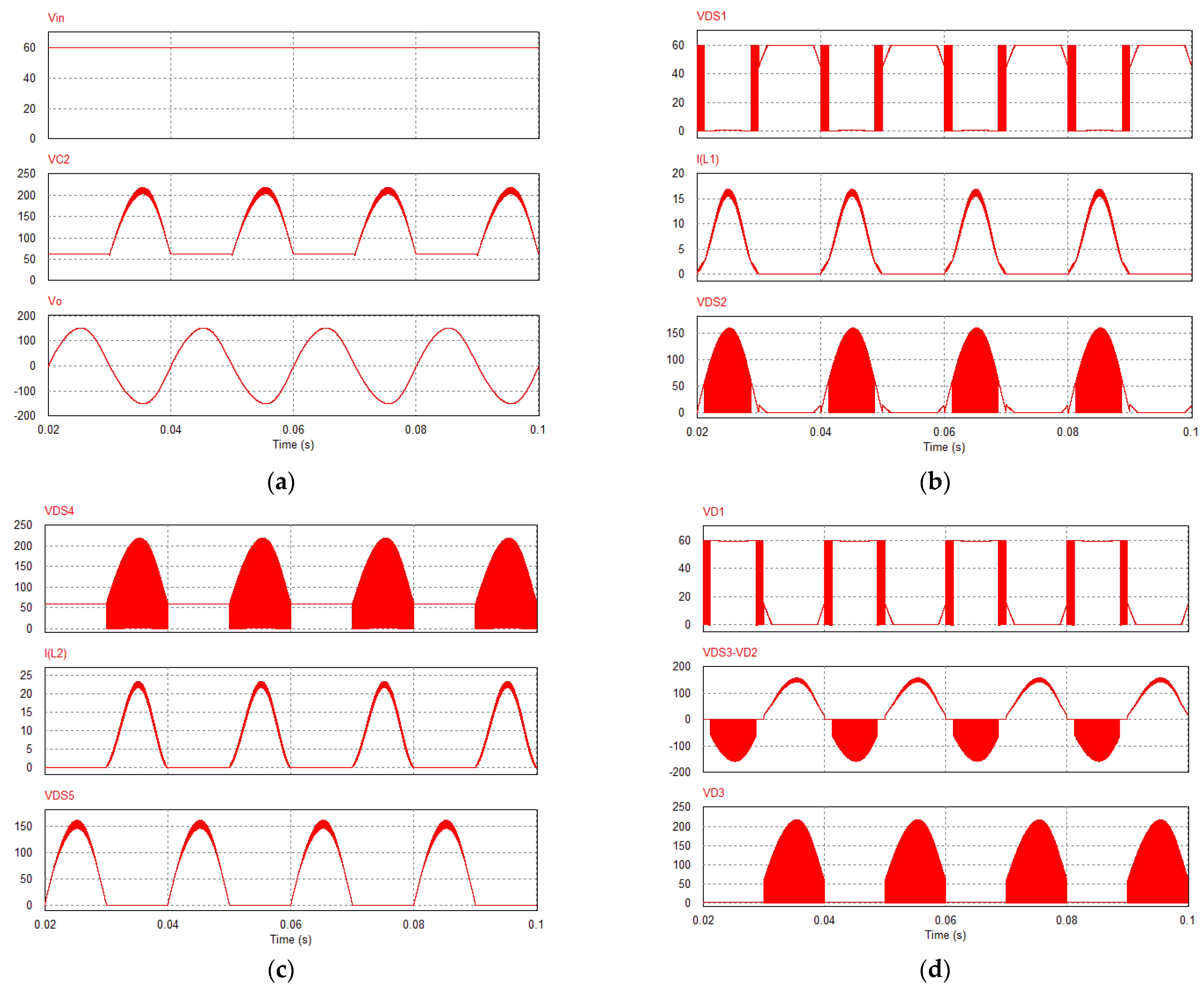
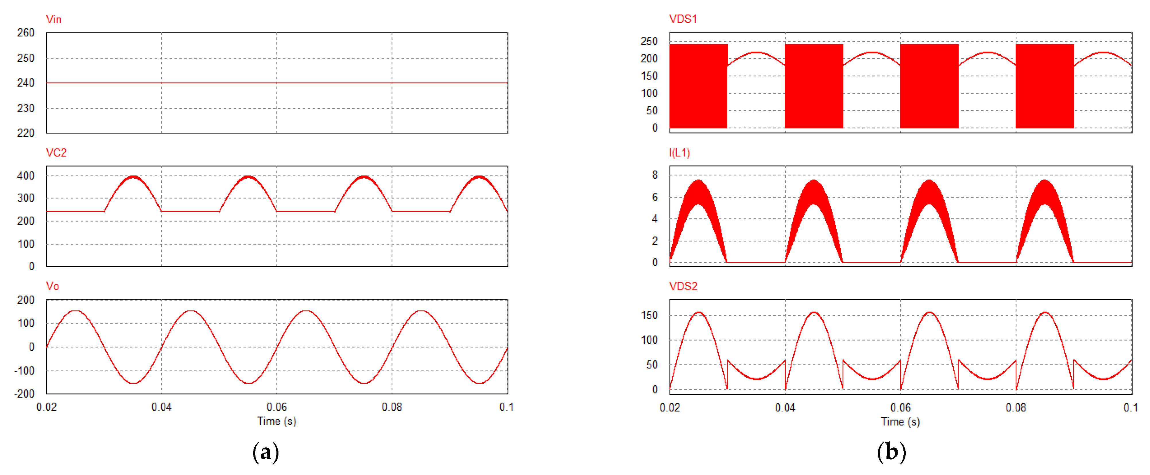
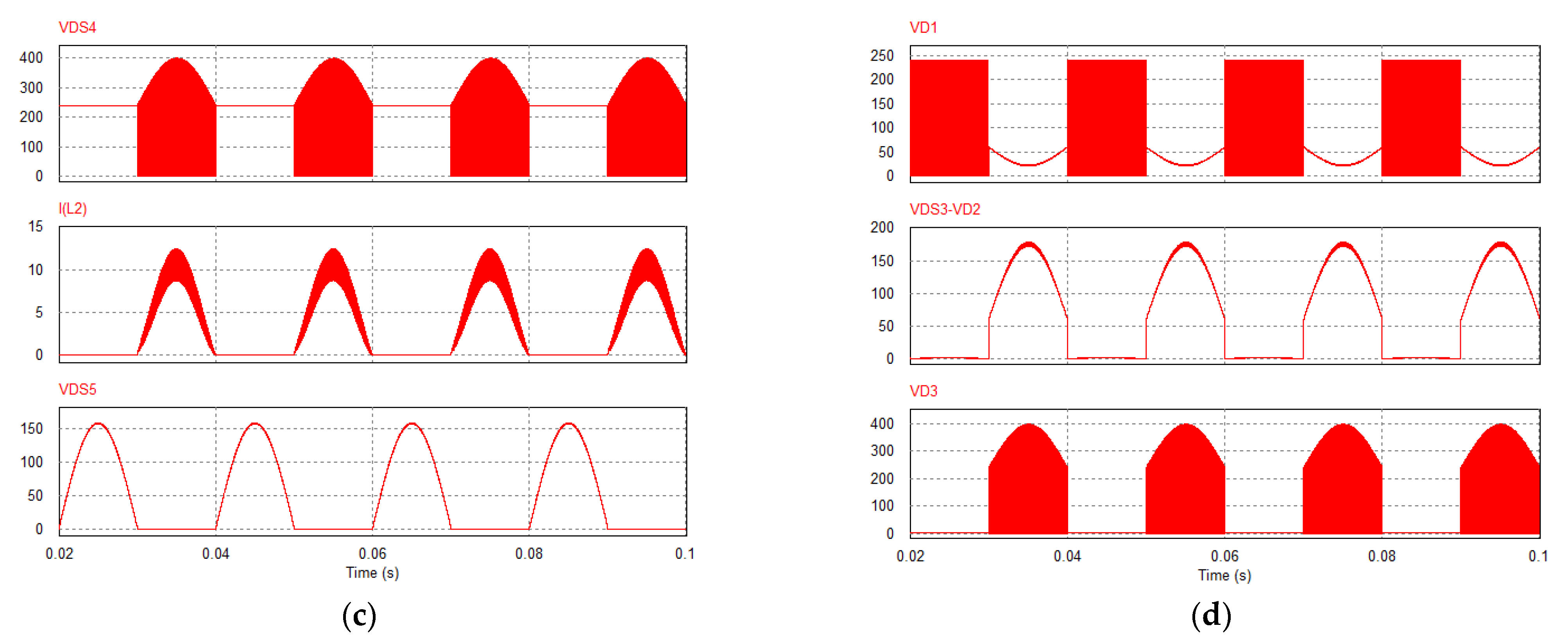
5.1. Simulation Results

The operating analysis of the proposed CGBBI topology was verified in the PSIM simulation version 9.1 [33]. The specifications for simulation are shown in Table 2. The drain-to-source on-resistance and body-diode threshold voltage of the MOSFETs S1, S4, and S2, S3, S5 were set to 25.5 mΩ, 45 mΩ, and 8 mΩ, respectively. The forward voltage of diodes D1 to D3 was set to 1.12 V, 0.7 V, and 1.4 V, respectively. Figure 6 and Figure 7 present the simulation waveforms of the proposed CGBBI topology in both buck and boost operations. The RMS values of the output voltage and output frequency were set at 110 V and 50 Hz. The input voltage values were 60 V and 240 V. In the case of Vin = 60 V, the modulation index and maximum values of duty cycles were M = 2.58, D1.max = 2.58, D2.max = 0.61, D4.max = 0.72. Additionally, with Vin = 240 V, the modulation index and maximum values of duty cycles were M = 0.64, D1.max = 0.64, D2.max = 0, D4.max = 0.39. The high-switching frequency of semiconductor devices was 50 kHz. From the design guideline in Section 3, the parameters of passive devices were chosen as follows: L1 = L2 = 0.5 mH, C1 = 5 µF, C2 = 1 µF. The input voltage, capacitor C2 voltage, output voltage, voltage stresses of semiconductor devices are shown in Figure 6 and Figure 7. Moreover, the THD values of the output voltage waveforms were measured at 1.2% and 0.5% for the input voltage of 60 V and 240 V, respectively. It can be observed that the simulation results well agreed with the theoretical analysis. The conduction and switching losses of the proposed CGBBI, together with the simulation results, are shown in Table 3. It can be seen that the simulation results are close to the power loss analysis.

5.2. Experimental Results

A 500 W prototype circuit was fabricated and tested to verify the performance of the proposed CGBBI topology. The specifications for testing are also shown in Table 2. Figure 8 presents the experimental waveforms of the proposed CGBBI topology when the inverter operated in boost mode. The maximum value of the output voltage was boosted to 155 V from an input voltage of 60 V, which corresponds to M = 2.58. Figure 8a shows the input voltage, capacitor C2 voltage, and output voltage for the load value of 24 Ω and filter inductor of 0.5 mH. The capacitor voltage VC2 was half-sinusoidal with DC offset Vin in the positive half of the output cycle. Therefore, the peak voltage across the capacitor C2 was approximately 220 V. In the negative half of the output cycle, the voltage across the capacitor C1 was equal to the input voltage. The RMS value and THD of the output voltage waveform were 109 V and 1.6%, respectively. Figure 8b shows the voltage stress on switches S1, S2, and the current of inductor L1. Figure 8c shows the voltage stress on switches S4, S5, and the current of inductor L2. The peak currents of inductors L1 and L2 were about 16 A and 23 A, respectively. The high-frequency ripple of inductors L1 and L2 current were about 2.5 A and 3 A, respectively. Figure 8d shows the voltage stress on diode D1, the voltage stress on switch diodes S3D2, and voltage stress on diode D3. Similarly, the proposed CGBBI topology was tested with an input voltage of 240 V, as shown in Figure 9. It can be seen that the experimental results are verified with the simulation and the theoretical analyses.
Moreover, the efficiency of the proposed CGBBI topology was measured at Vin = 60 V and Vin = 240 V. In this case, the output power of the inverter changed from 25 W to 500 W. When Vin = 240 V, the proposed CGBBI topology achieved the highest efficiency of 96.1%. When the input voltage decreased to 60 V, the efficiency of the proposed CGBBI topology also achieved the highest efficiency of 95% at 350 W. From Figure 10, the EU efficiency of the proposed CGBBI topology can be obtained at 95.24%. The parameters for the power losses calculation are presented in Table 4. Figure 11 depicts the power loss distribution of the proposed CGBBI when Vin = 60 V and 240 V, vo = 110 Vrms, and Po = 500 W.

6. Conclusions

In this article, a common-ground buck–boost inverter topology was introduced, and its theoretical analysis was discussed in detail. In the proposed inverter, there is no common-mode leakage current because the ground of the output side is directly connected to the negative of the DC input power source. The proposed common-ground buck–boost inverter topology also provides buck–boost capability by controlling the duty cycle of power switches. In addition, few power switches operated with high-switching frequency, so the efficiency of the proposed inverter can be improved. Furthermore, the simulation and experimental verification were presented with a 500 W prototype inverter. The results highlighted that the proposed inverter can steadily operate and have good performance.

Author Contributions

D.-V.V. determined topology and prepared the original draft. M.-K.N. contributed to the manuscript’s review and editing. T.-D.D. contributed to validating the simulation work. T.-T.T. contributed to validating the experimental work. Y.-C.L. provided resources and supervision. J.-H.C. provided resources and funding acquisition. All authors have read and agreed to the published version of the manuscript.

Funding

This research received no external funding.

Institutional Review Board Statement

Not applicable.

Informed Consent Statement

Not applicable.

Data Availability Statement

Data are contained within the article.

Conflicts of Interest

The authors declare no conflict of interest.

References

  1. Jo, K.-Y.; Duong, T.-D.; Choi, J.-H. Emerging Technologies in Power Systems. Electronics 2022, 11, 71. [Google Scholar] [CrossRef]
  2. Sarvar, H.N.; Muhammad, U.A.; Zafar, A.; Sadam, H.; Tahir, M.; Muhammad, J.A.; Raghavendra, K.V.G.; Kim, H.J. An Optimized Methodology for a Hybrid Photo-Voltaic and Energy Storage System Connected to a Low-Voltage Grid. Electronics 2019, 8, 2. [Google Scholar]
  3. Mattia, F.; Marta, M.; Eneko, O.O. A flexible power electronics configuration for coupling renewable energy sources. Electronics 2015, 4, 2. [Google Scholar]
  4. Duong, T.-D.; Nguyen, M.-K.; Tran, T.-T.; Lim, Y.-C.; Choi, J.-H. Transformerless High Step-Up DC-DC Converters with Switched-Capacitor Network. Electronics 2019, 8, 1420. [Google Scholar] [CrossRef] [Green Version]
  5. Kouro, S.; Leon, J.I.; Vinnikov, D.; Franquelo, L.G. Grid-connected photovoltaic systems: An overview of recent research and emerging PV converter technology. IEEE Ind. Electron. Mag. 2015, 9, 47–61. [Google Scholar] [CrossRef]
  6. Alluhaybi, K.; Batarseh, I.; Hu, H. Comprehensive Review and Comparison of Single-Phase Grid-Tied Photovoltaic Microinverters. IEEE J. Emerg. Sel. Top. Power Electron. 2020, 8, 1310–1329. [Google Scholar] [CrossRef]
  7. Chiu, H.; Lo, Y.; Yang, C.; Cheng, S.; Huang, C.; Kou, M.; Huang, Y.; Jean, Y.; Huang, Y. A module-integrated isolated solar micro-inverter. IEEE Trans. Ind. Electron. 2013, 60, 781–788. [Google Scholar] [CrossRef]
  8. Meneses, F.; Blaabjerg, X.E.; Garc, O.A.; Cobos, J.A. Review and comparison of step-up transformerless topologies for photovoltaic ac module application. IEEE Trans. Power Electron. 2013, 28, 2649–2663. [Google Scholar] [CrossRef] [Green Version]
  9. Li, W.; Gu, Y.; Luo, H.; Cui, W.; He, X.; Xia, C. Topology Review and Derivation Methodology of Single-Phase Transformerless Photovoltaic Inverters for Leakage Current Suppression. IEEE Trans. Ind. Electron. 2015, 62, 4537–4551. [Google Scholar] [CrossRef]
  10. Barater, D.; Lorenzani, E.; Concari, C.; Franceschini, G.; Buticchi, G. Recent advances in single-phase transformerless photovoltaic inverters. IET Renew. Power Gener. 2016, 10, 260–273. [Google Scholar] [CrossRef]
  11. IEC Standard 61727-2004; Photovoltaic (PV) Systems—Characteristics of the Utility Interface. International Electrotechnical Commission (IEC): Geneva, Switzerland, 2004.
  12. IEEE Standard 1547.2-2008; IEEE Standard for Interconnecting Distributed Resources with Electric Power Systems. IEEE Application Guide for IEEE Std 1547. IEEE: New York, NY, USA, 2009; pp. 1–207.
  13. Nimrod, V.; Jeziel, V.; Joaquin, V.; Claudia, H.; Esli, V.; Rene, O. Integrating two stages as a common-mode transformerless photovoltaic converter. IEEE Ind. Electron. 2017, 64, 7498–7507. [Google Scholar]
  14. Vázquez, N.; Rosas, M.; Hernández, C.; Vázquez, E.; Perez-Pinal, F. A new common-mode transformerless photovoltaic inverter. IEEE Trans. Ind. Electron. 2015, 62, 6381–6391. [Google Scholar] [CrossRef]
  15. Arshadi, S.A.; Poorali, B.; Farzanehfard, H. High step-up dc–ac inverter suitable for ac module applications. IEEE Trans. Ind. Electron. 2016, 63, 832–839. [Google Scholar] [CrossRef]
  16. Wu, T.-F.; Chang, C.-H.; Lin, L.-C.; Kuo, C.-L. Power loss comparison of single-stage and two-stage grid-connected photovoltaic systems. IEEE Trans. Energy Convers. 2011, 26, 707–715. [Google Scholar] [CrossRef]
  17. Hu, H.; Harb, S.; Kutkut, N.H.; Shen, Z.J.; Batarseh, I. A single-stage microinverter without using electrolytic capacitors. IEEE Trans. Power Electron. 2013, 28, 2677–2687. [Google Scholar] [CrossRef]
  18. Choi, W.-Y.; Yang, M.-K. Transformerless Quasi-Z-Source Inverter to Reduce Leakage Current for Single-Phase Grid-Tied Applications. Electronics 2019, 8, 312. [Google Scholar] [CrossRef] [Green Version]
  19. Xia, Y.; Roy, J.; Ayyanar, R. A capacitance-minimized doubly grounded transformer less photovoltaic inverter with inherent active power decoupling. IEEE Trans. Power Electron. 2017, 32, 5188–5201. [Google Scholar] [CrossRef]
  20. Yao, Z.; Zhang, Y.; Hu, X. Transformerless grid-connected PV inverter without common mode leakage current and shoot-through problems. IEEE Trans. Circuits Syst. II Exp. Briefs. 2020, 67, 3257–3261. [Google Scholar] [CrossRef]
  21. Wang, H.; Lu, Z. A New Converter for Non-Isolated PV Systems. Electronics 2021, 10, 1716. [Google Scholar] [CrossRef]
  22. Weimin, W.; Junhao, J.; Frede, B. Aalborg Inverter—A New Type of “Buck in Buck, Boost in Boost” Grid-Tied Inverter. IEEE Power. Electron. 2015, 30, 4784–9827. [Google Scholar]
  23. Xuefeng, H.; Penghui, M.; Benbao, G.; Meng, Z. An integrated step-up inverter without transformer and leakage current for grid-connected photovoltaic system. IEEE Power. Electron. 2019, 34, 9814–9827. [Google Scholar]
  24. Hafiz, F.A.; Mohamed, S.E.M.; Bashar, Z.; Khalifa, A.H. Single-phase photovoltaic inverters with common-ground and wide buck–boost voltage operation. IEEE Ind. Inform. 2021, 17, 8275–8287. [Google Scholar]
  25. Hiren, P.; Vivek, A. A single-stage single-phase transformer-less doubly grounded grid-connected PV interface. IEEE Energy Conversion. 2009, 24, 93–101. [Google Scholar]
  26. Mehdi, T.T.; Mehran, S.; Ebrahim, B.; Farhad, A.A.M. Modified Single-Phase Single-Stage Grid-Tied Flying Inductor Inverter with MPPT and Suppressed Leakage Current. IEEE Ind. Electron. 2018, 65, 221–231. [Google Scholar]
  27. Phani, K.C.; Mohamed, S.E.M.; Vinod, K.; Khalifa, H.A.H.; Tarek, H.M.E.F. Novel Step-Up Transformerless Inverter Topology for 1-Φ Grid-Connected Photovoltaic System. IEEE Ind. Appl. 2021, 57, 2801–2815. [Google Scholar]
  28. Lee, S.-S.; Gorla, N.-B.-Y.; Sanjib, K.-P.; Lee, K.-B.; Yam, P.-S.; Reze, B. A Common-Ground-Type Single-Stage Buck-Boost Inverter with Sinusoidal Output Voltage. In Proceedings of the ICPE-ECCE Asia, Singapore, 10–14 October 2021; pp. 397–401. [Google Scholar]
  29. Naser, V.; Seyed, H.-H.; Mehran, S. A New Single-Phase Transformerless Grid-Connected Inverter with Boosting Ability and Common Ground Feature. IEEE Ind. Electron. 2020, 67, 9313–9325. [Google Scholar]
  30. Zhilei, Y.; Zhong, W. Single-Stage Doubly Grounded Transformerless PV Grid-Connected Inverter with Boost Function. IEEE Power Electron. 2022, 37, 2237–2249. [Google Scholar]
  31. Kazimierczuk, M.K.; Sekiya, H. Design of AC resonant inductors using area product method. In Proceedings of the 2009 IEEE Energy Conversion Congress and Exposition, San Jose, CA, USA, 20–24 September 2009. [Google Scholar]
  32. Wang, Q.; Gao, T. Simulation. In Proceedings of the IEEE 2017 International Conference on Computer Network, Electronicand Automation (ICCNEA), Xi’an, China, 23–25 September 2017; pp. 336–340. [Google Scholar]
  33. Górecki, P.; Górecki, K. Methods of Fast Analysis of DC–DC Converters—A Review. Electronics 2021, 10, 2920. [Google Scholar] [CrossRef]
Figure 1. Proposed single-stage common-ground buck–boost inverter.
Electronics 11 00829 g001
Figure 2. PWM control method of the proposed CGBBI topology.
Electronics 11 00829 g002
Figure 3. Equivalent circuits of the proposed CGBBI topology in interval 1 when 0 < vo < Vin: (a) mode 1 and (b) mode 2.
Electronics 11 00829 g003
Figure 4. Equivalent circuits of the proposed CGBBI topology in interval 2 when vo > Vin: (a) mode 1 and (b) mode 2.
Electronics 11 00829 g004
Figure 5. Equivalent circuits of the proposed CGBBI topology in interval 3 when vo < 0: (a) mode 1 and (b) mode 2.
Electronics 11 00829 g005
Figure 6. Simulation results with Vin = 60 V: (a) the input, output and capacitor C2 voltages, (b) the voltage stress on switches S1, S2, and the current of inductor L1, (c) the voltage stress on switches S4, S5, and the current of inductor L2, and (d) the voltage stress on diodes D1, D2, D3 and the voltage stress on switch S3.
Electronics 11 00829 g006
Figure 7. Simulation results with Vin = 240 V. (a) the input, output and capacitor C2 voltages, (b) the voltage stress on switches S1, S2, and the current of inductor L1, (c) the voltage stress on switches S4, S5, and the current of inductor L2, and (d) the voltage stress on diodes D1, D2, D3 and the voltage stress on switch S3.
Electronics 11 00829 g007aElectronics 11 00829 g007b
Figure 8. Experimental results with Vin = 60 V. (a) the input, output and capacitor C2 voltages, (b) the voltage stress on switches S1, S2, and the current of inductor L1, (c) the voltage stress on switches S4, S5, and the current of inductor L2, and (d) the voltage stress on diodes D1, D2, D3 and the voltage stress on switch S3.
Electronics 11 00829 g008aElectronics 11 00829 g008b
Figure 9. Experimental results with Vin = 240 V. (a) the input, output and capacitor C2 voltages, (b) the voltage stress on switches S1, S2, and the current of inductor L1, (c) the voltage stress on switches S4, S5, and the current of inductor L2, and (d) the voltage stress on diodes D1, D2, D3 and the voltage stress on switch S3.
Electronics 11 00829 g009aElectronics 11 00829 g009b
Figure 10. Efficiency measurement with Vin = 60 V and Vin = 240 V.
Electronics 11 00829 g010
Figure 11. Power loss distribution of the proposed CGBBI.
Electronics 11 00829 g011
Table 1. Comparison between the proposed CGBBI topology and other common-ground transformerless inverters.
Inverter in [21]Inverter in [22]Inverter in [23]Inverter in [24]Inverter in [25]Inverter in [28]Inverter in [29]Inverter in [30]Proposed CGBBI
Switches465558755
Diodes250430133
Inductors222521022
Capacitors212321222
Total devices10149171210101212
Switches stressS1 to S4: 2VoS1, S4: Vin
S2, S3: Vo
S5, S6: Vo
S1 to S5:
Vin + Vo
S1 to S5:
Vin + Vo
S1: Vin + Vo
S2 to S5: Vo
S1: Vin
S2: Vo
S3: Vin
S4, S7: Vin + Vo
S5: Vo
S6, S8: Vo
S1, S2: Vin
S3: 3Vin
S4, S5: 2Vin
S6: 2Vin
S7: 4Vin
S1, S2: Vin + Vo
S3, S4: Vo
S5: Vo
S1: Vin
S2, S3, S5: Vo
S4: Vin + Vo
HF-switches in each period4P
4N
3P
3N
2P
2N
3P
1N
3P
1N
5P
3N
4P
5N
2P
1N
2P
1N
Diodes stress-D1, D4: Vin
D2, D3, D5: Vo
-D1 to D4:
Vin + Vo
D1: Vin + Vo
D2: Vin
D3: Vo
-D: VinD1: Vo
D2: Vin + Vo
D3: VoVin
D1: Vin
D2: Vo
D3: Vin + Vo
P and N are the number of high-frequency switching in positive and negative half-line periods, respectively.
Table 2. Parameters of the proposed CGBBI topology.
ParameterSymbolPart No./Value
Input voltage rangeVin60–240 V
Output Voltagevo110 Vrms
Output frequencyfo50 Hz
Output PowerPo500 W
Switching frequencyfsw50 kHz
CapacitorsC15 µF/200 V
C21 µF/450 V
InductorsL1, L20.5 mH
Filter inductorLf0.5 mH
MOSFETsS1IRFP4868PbF (300 V, 70 A, Rdson = 25.5 mΩ)
S2, S3, S5IRFP4668PbF (200 V, 130 A, Rdson = 8 mΩ)
S4IPW60R045CPA (600 V, 60 A, Rdson = 45 mΩ)
DiodesD1FF60UP30DN (300 V, 60 A, VF = 1.12 V)
D2STPS60SM200C (200 V, 30 A, VF = 0.7 V)
D3DSEI30-06A (600 V, 37 A, VF = 1.4 V)
Table 3. The power loss of the proposed CGBBI with simulation.
ComponentsVin = 60 VVin = 240 V
Currents (A)Losses (W)Currents (A)Losses (W)
AverageRMSConductionSwitchingAverageRMSConductionSwitching
S14.17.081.280.751.042.40.151.25
S22.145.330.232.970000
S324.670.172.772.053.260.092.84
S44.128.533.271.331.032.990.41.63
S524.540.162.772.053.650.112.84
D15.24 × 10−20.260.060.031.012.191.280.13
D224.671.902.053.261.680
D325.624.380.942.064.053.71.73
L14.157.092.01-2.053.250.42-
L26.1210.224.18-3.095.041.02-
C11.9 × 10−34.770.11-3.86 × 10−31.770.02-
C29.22 × 10−31.480-9.32 × 10−30.770-
Ploss--29.31--19.29
Table 4. Parameters for power loss analysis.
ParametersValues
Inductors L1, L2CoreCM777125 (142 nH/N2)
Parastic Resistor40 mΩ
CapacitorsESR of C1 49 mΩ
ESR of C214 mΩ
MOSFETs IRFP4668PbF (200 V, 130 A, Rdson = 8 mΩ)
IRFP4868PbF (300 V, 70 A, Rdson = 25.5 mΩ)
IPW60R045CPA (600 V, 60 A, Rdson = 45 mΩ)
DiodesSTPS60SM200C (200 V, 30 A, VF = 0.7 V)
FF60UP30DN (300 V, 60 A, VF = 1.12 V)
DSEI30-06A (600 V, 37 A, VF = 1.4 V)
Publisher’s Note: MDPI stays neutral with regard to jurisdictional claims in published maps and institutional affiliations.

