1. Introduction
In recent years, a considerable portion of the electronics field has been focused on bioengineering applications. The modern internet of medical things (IoMTs) or the body area networks (BANs), as well as the less recent implantable neural prostheses, are proof that more and more attention is being paid to these kinds of applications. Looking to neurological and mental disorders, their impacts can often be alleviated by bioelectronics and neuroprosthetics medicine. Implantable neural prostheses, such as deep brain the Ref. [
1], cortical [
2] or nerve [
3] stimulators and cochlear implants [
4] are examples of clinically adopted neuro-technology to revert impaired or lost functions.
In general clinically adopted implantable neural prostheses, a micro-electrode array is kept in contact with the tissue and it is electrically linked, often by using cables, to a unit aimed at recording neuronal activities and/or for neural stimulation. The design principle has its roots back to the first fully implantable battery-powered pacemaker [
5]. Since then, several variations of this design principle were used in many successful applications, despite having several critical limitations. For instance, the excessive intrusiveness and mechanical stresses that cables and connectors can have on human tissues are weak points of the system, often leading to failure. Moreover, due to its size, the implanted unit cannot be located close to the target tissue. Instead, it is placed in a remote location and wires are used to connect them to micro-electrode arrays for stimulation.
To get rid of this drawback, more recently adopted implantable neurostimulators have employed a wireless link for power and data transfer from/to the implanted IC. This constitutes a technological challenge in neurostimulation, whose state-of-the-art culminates with arrays of free-standing smart electrodes, not relying on powered units and wired connections [
6]. Such smart electrodes should integrate all the required elements to receive power and operational commands (downlink communication), while the preserve size should be compatible with the intended application, ideally smaller than 1
. For this reason, the miniaturisation of the implantable device is crucial to achieve safe and noninvasive surgical implantation. Such a system is better-known with the acronym IMD, which stands for an “implanted medical device”.
In this framework, as a part of wireless IMDs, we propose a new solution of a Binary Phase-Shift Keying (BPSK) demodulator in order to design a robust, low-area and low-power downlink for ultrasound (US)-powered implanted units. The implemented system is fully digital and PLL-free, thus reducing area occupation and making it fully synthesizable. Simulation results are reported using a 28 nm Bulk CMOS technology provided by TSMC.
The paper is organized as follows.
Section 2 reports a system overview of US-powered implanted medical devices. Then, starting from the US-link characterization shown in
Section 3, the proposed fully digital BPSK demodulator is introduced and described in each single block in
Section 4.
Section 5 shows post-layout simulation results of the proposed circuit as also compared with the state-of-the-art. Finally, the last section reports the conclusions of this work.
2. US-Powered IMDs: A System Overview
The system represented in
Figure 1 is an illustrative description of the US-powered integrated circuit to be implanted in the human brain. It is worth noting that the same IC could be used for any specific biomedical application, such as heart-beat stimulations, gastrointestinal activities manipulation, and other kinds of controls and actuations applied to patients affected by chronic diseases [
7,
8,
9,
10]. The IMDs are powered-up, exploiting US-acoustic waves generated from external piezo-transducers (
TX-PIEZO, in
Figure 1) kept under the electrical resonance condition and placed in contact with the skin. Thus, once the acoustic waves reach the depth of a second power-receiving piezo-transducer (
RX-PIEZO), they can be efficiently rectified and conditioned to power up a storage capacitor, namely C
STOR, in the Figure mentioned above. In fact, the described system is battery-less and plainly covers the concept of Energy Harvesting, exploiting the electro-acoustic coupling of two small, thick and low-invasive piezoelectric devices.
As depicted in most of the works presented in the literature on the Power Management Integrated Circuit (PMIC) for Energy Harvesting systems, as reviewed in the Ref. [
11], the power conditioning circuit is often made up of an impedance matching network [
12], an active AC/DC converter [
13,
14], a voltage reference [
15] and a low-dropout voltage regulator (LDO) [
16] that provides a regulated rectified voltage (i.e.,
V in
Figure 1). Moreover, starting from the experimental measurements conducted by the authors, a diode-clamping circuit could be necessary for those cases in which the maximum voltage amplitude raises the maximum allowable voltage for the adopted IC technology. Moreover, a Power-On Reset (POR) circuit, as the one shown in the Ref. [
17], is often needed to enable/disable the load circuitry.
On the other hand, two further subsections are presented in
Figure 1, namely, the demodulator and stimulation circuit, both powered by the PMIC. Indeed, the presence of a communication sub-system for an IMD is mandatory, since it allows to establish data communication between the IMDs and the external world for long-term monitoring and stimulation purposes. In particular, the feature of collecting data and communicating them to the external world, namely Data Up-Link, has revealed a promising solution for bioelectronic medicine that exploits these devices [
7]. Furthermore, the ability to act on neurons, nerves, the heart-beat, and gastrointestinal activities, made up through the manipulation of electrical transducers, could optimise therapeutic protocols and help relieve patients’ pain [
10]. These kinds of stimulations come from the modulation of a powering signal generated from an externally placed unit coupled to the implanted receivers for power/data exchanging. The established communication is also defined as a Data Down-Link. Thus, an incoming-signal demodulator is needed to acquire an external signal to properly drive the above-mentioned electrical transducers. Then, the received information is elaborated into an implanted processing unit (i.e., a Digital Signal Processor, DSP, or a Field Programmable Gate array, FPGA) that works together with a Digital-to-Analog Converter (DAC), allowing for the electrical stimulation of the nerves/brain, as schematically represented in
Figure 1.
This work mainly concerns the design of a US-Data Down-Link embedding the proposed fully digital BPSK demodulator. Indeed, the state-of-the-art presents several modulation schemes, such as the ASK [
18,
19], PWM-ASK [
20], OOK [
19,
21,
22], and OOK-PM [
23,
24], while the BPSK demodulation has often been used for RF-powered IMDs [
25,
26,
27,
28,
29,
30,
31].
The choice of this modulation scheme arises from three main reasons. The first one regards the presence of a clamping circuit that often makes the amplitude demodulation on the incoming acoustic waves difficult; indeed, a variation of the voltage amplitude on the driving
TX-PIEZO could not be proficiently detected once impinged on the implanted IC. The second motivation is the necessity of a continuous powering of the IMDs, making the efficient use of the On–Off Shift Keying (OOK) proposed in the Refs. [
19,
21,
22] difficult. Finally, the last motivation arises from inspection of the graph reported in
Figure 2. It shows the Bit-Error-Rate (BER) for different modulation schemes as a function of the Signal-to-Noise Ratio (SNR) defined as the ratio
, where
is the energy-per-bit and
is the noise power. Specifically, the compared schemes modulate the received signal amplitude (BASK), its frequency (BFSK), its phase (BPSK) or its phase with differential modulation (DPSK). It is possible to observe that the BPSK presents the lowest BER, for a given value of the SNR. Furthermore, if the BPSK demodulation system does not require any synchronization between the data transmitter and the data receiver, it is defined as a non-coherent BPSK modulation.
Assuming BPSK modulated the input signal, the external powering and modulating electronic system depicted in the left-most side of
Figure 1 is essentially based on an FPGA that generates the sinusoidal signal at the piezo-transducers electrical resonance frequency,
, as well as a power amplifier (PA) which drives the
TX-PIEZO with the suitable power level.
The FPGA acts as a modulator exploiting a proper digital signal, named
MOD, that exchanges the two sinusoidal phases,
and
, generating the following transmitted signal
As shown in
Figure 1, the implanted demodulator of the integrated system requires a robust oscillator (i.e., current starved ring (CSRO) oscillator, as proposed in the Ref. [
6]). However, it is worth noting that the internal oscillator of the implanted processing unit could be equivalently used, thus reducing both the area occupation and the power consumption of the entire data-receiving system.
3. Characterization of the US Data Link
Since the features of links for power and data transfer determine part of the specifications for the all the implemented devices and, in particular, for PMIC and the demodulator, this section focuses on its characterization. It consists of two piezoelectric devices. The first one is the power transmitting piezo, TX PIEZO, which is placed outside the body and used to transfer power and transmit data to the implanted device (down-link); the other one is the RX PIEZO which, as indicated in
Figure 1, is implanted together with the entire IC. It harvests the transferred power, receives data, and is also used to send data to the outside device (up-link). US-piezo receivers were selected among the ones present on the market, trying to carry out the best trade-off between dimensions, operating frequency, and the maximum transferable power. As per the results of previously conducted studies, the operating frequency under an electrical resonance condition was selected to be equal to
∼ 2 MHz, for both piezoelectric devices, with a thickness,
t, of about 0.4–0.5 mm for the receiving piezo. This choice was due to a trade-off between the miniaturization requirement and the harvested power. In order to emulate the acoustic impedance of body tissues, ballistic gel was used. This solution was already adopted in various medical fields, such as the anthropomorphic cardiac phantom for ultrasound imaging, and thanks to its acoustic properties, and compatibility with conventional plastics molding techniques, it has been designated as among the best materials for tissue-mimicking [
34]. Considering that both piezoelectric transducers should be separated by a physical sandwich composed by the skin, vessels, and cerebral cortex, the distance between them should be in the order of
d = 0.5–1.5 cm; in this way, both the devices are encapsulated in ballistic gel, keeping such a distance fixed.
As for the materials selection, they are the same as that used in the Ref. [
14]. The TX-PIEZO is the PRY+0111 provided by PI Ceramics. It is made up by a disk of PIC255 with a diameter equal to 10 mm, with a radial resonant frequency equal to 250 kHz and a transverse resonance frequency equal to 2 MHz. As for the RX-PIEZO, it is the 000065944 provided by the same manufacturer. It is a thin layer of PIC255, with a square form whose area is equal to 9 mm
and a thickness of
t = 0.5 mm; its radial resonance frequency is placed at 500 kHz, while its transverse resonant frequency is about 2 MHz.
Figure 3 and
Figure 4 show the US-data link for testing and the RX-PZT. In detail,
Figure 3 shows the encapsulation in ballistic gel with a fixed distance,
cm between the RX-PZT and the TX-PZT to mimic the acoustic impedance of tissues, while
Figure 4 presents the block diagram of the experimental measurement setup used for the characterization of the US-power link. A signal generator was used to drive the RX-PZT with a 20-
sinusoidal signal, while an oscilloscope measured the received electrical signal over the TX-PZT.
Let us now consider the definition of wavelength;
, when
MHz and
m/s, it follows that
mm. It means that the distance
1–1.5 cm is quite large compared to the US-wavelength in tissues, so the waves propagate in a far-field region. This is further demonstrated by considering (
2). In fact, it is worth remembering that the distance between the last sound pressure’s maximum value and the sound source is called the near-field length, which is expressed by
N, and the area within the
N is called the near-field area. The region where the distance from the axis of the wave source is greater than the length of the near-field region is called thefar-field region. The ultrasonic near-field area can be calculated by the following equation [
35]:
where
D is the diameter of the material, and
A, its area, equals to about 9 mm
, while
is the US-wavelength in tissues. This proves that the system works in the far-field region.
The impedance characterization of the devices was carried out using a VNA (E5061B provided by Keysight Technologies), measuring out both the magnitude of the impedance,
, and the phase
as functions of the frequency. Both piezo devices were connected to the VNA, and the equivalent Butterworth–Van Dyke (BVD) electric circuits were carried out. Furthermore, resonance doublets were depicted by using two parallel RLC series circuits but, as claimed before, for the power transfer to the implanted device, just the electric resonance is important. The piezo devices, under the electrical resonance condition, presents finite impedances (in the order of magnitude of 0.1–1 k
), when acting as a passive component (e.g., the TX-PIEZO). On the other hand, the Thévenin equivalent model deals with the concept of active generation when resonance for the RLC series circuit occurs (see
Figure 5c)). The received voltage amplitude falls in the following range
V, while the received power in
mW and the equivalent series resistance is
k
. A peak-to-peak sine signal applied to the TX-PZT equals to 20
, and the electrical resonance frequency is the same as that of the RX-PZT,
MHz.
4. The Proposed Fully Digital BPSK Demodulator
The Binary Phase Shift Keying (BPSK) is the most famous PSK modulation, and the most widely adopted method to recover data from a BPSK signal is the Costas loop for coherent modulation schemes [
36]. As explained in the Ref. [
25], the above-cited loop consists of two parallel phase-locked loops (PLLs), where one is called the
in-phase loop, IPL, and the other is called the
quadrature-phase loop, QPL. Their phase error outputs are multiplied to control the frequency of the oscillator. The square term of the data stream makes the control signal proportional to the phase difference as the conventional PLL and, in the locked state, the output at the in-phase branch becomes the demodulated signal. Generally, a four-quadrant analog multiplier is adopted to realize the I/Q arm phase detector and the multiplier in the voltage-controlled oscillator (VCO) branch. Such complexity in terms of the needed circuitry constitutes the main drawback of the conventional
Costas loops for BPSK demodulators, limiting its use in practical applications.
On the other hand, recent works have exploited digital architectures for BPSK demodulation [
26,
28,
30,
31]. Many schemes have adopted a 1-bit Analog-to-Digital Converter (ADC) implemented with Schmitt’s Triggers, a clock-recovery circuit and D-Flip-Flops (DFFs) whose role is as frequency dividers or as counters. However, it is important to underline that most of them present a
non-coherent demodulation scheme, since phase synchronization is not required with the source of the modulated signal.
The system proposed in this paper falls within the last family.
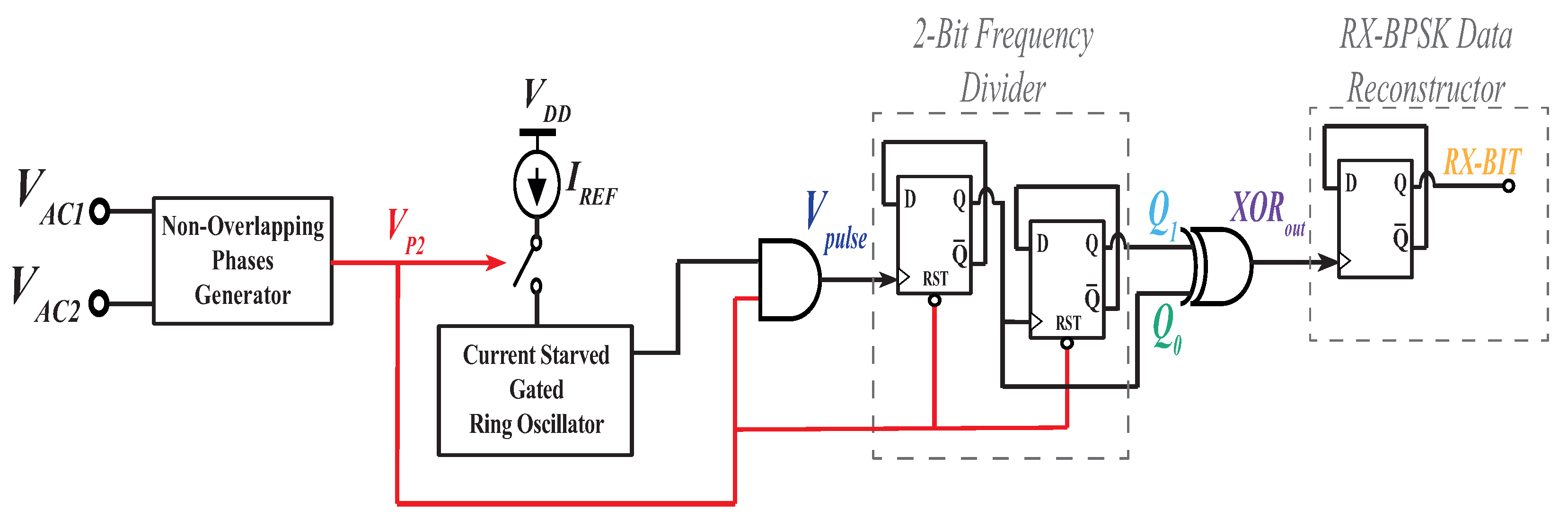
Figure 6 shows the simplified block diagram of the whole BPSK demodulator and its working principle is explained in the following, with the help of the timing diagram reported in
Figure 7.
The two input sinusoidal waves that come out from the
RX-PIEZO are firstly clamped out, and, consequently, they degenerate two semi-square waveform signals, namely
V, in
Figure 6. When the phase modulation occurs, one of the two phases will present a doubled time duration. In this paper, just the negative sine phase,
, is taken into account as the incoming modulation signal is high (i.e.,
MOD in Equation (
1) is high).
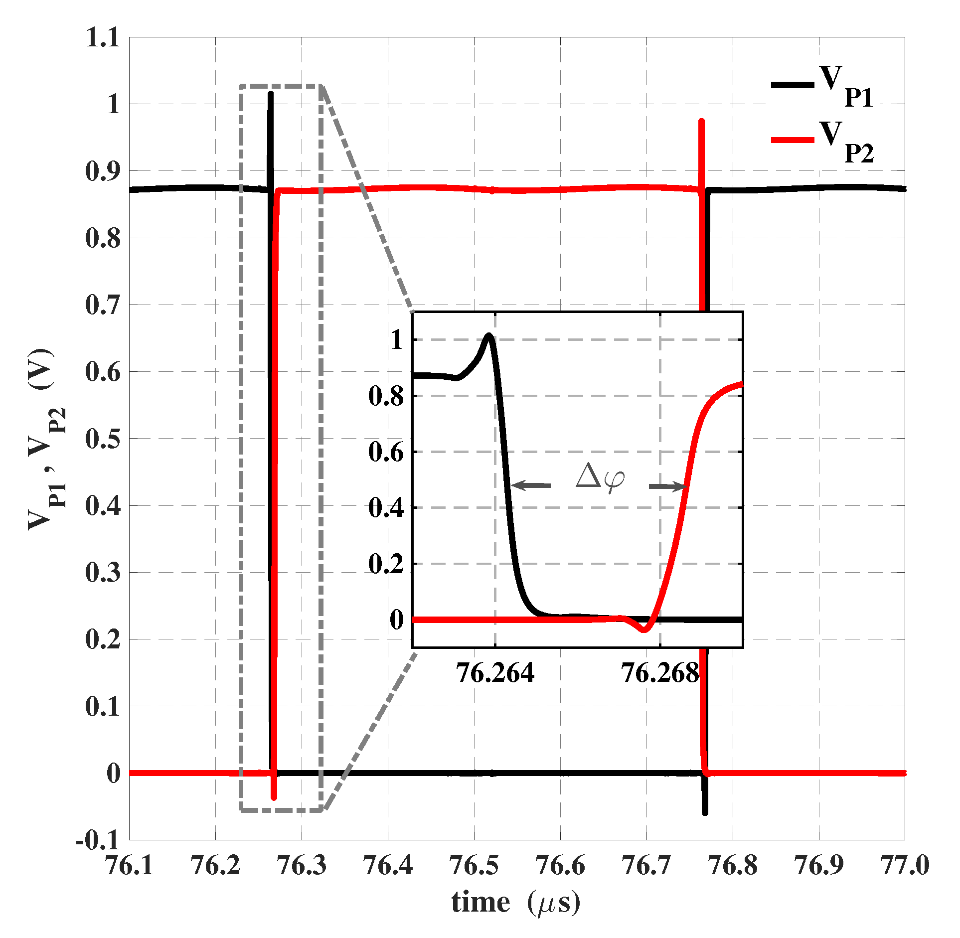
A non-overlapping phase generator is strongly required, since it allows to better separate and distinguish, from a temporal point of view, the two clamped-sine incoming phases and to detect the bit-start/end signals. Moreover, its output, , is the resulting modulating phase.
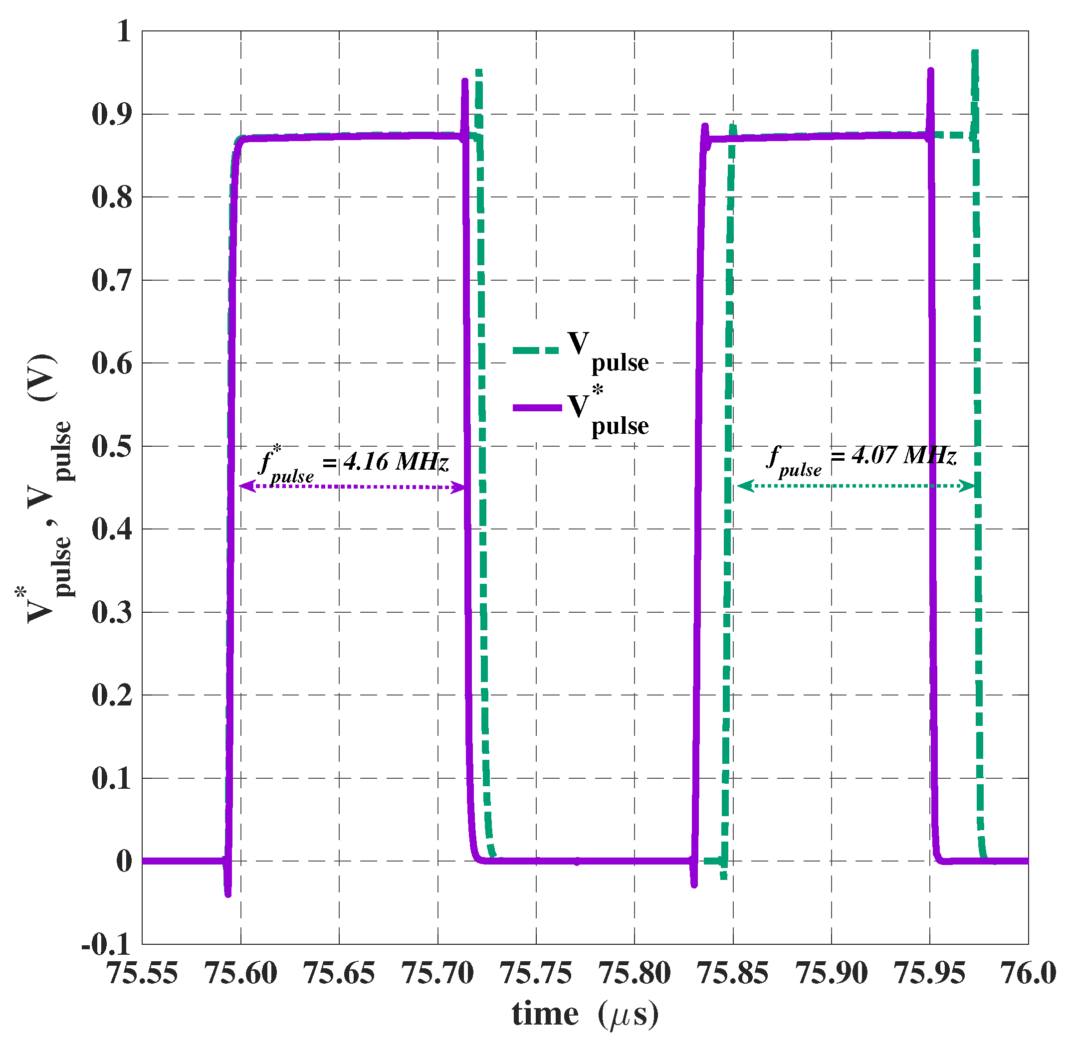
A current-starved ring oscillator starts oscillating just when the enabling phase () is high.
The core of the proposed demodulator is constituted by a 2-bit frequency divider and a CMOS XOR gate which allows to count the number of pulses generated by the ring oscillator, when enabled by . Briefly, the changes in the output bit state happen when a doubling on the number of pulses of the oscillator occurs (i.e., two clock pulses are generated when MOD goes high and, vice-versa, a single clock pulse when no modulation occurs). In such event, the two output states and will present different time durations, and this difference will be detected by the XOR gate.
The pulses generated by the XOR gate,
, which are slightly delayed as indicated
in
Figure 7, allows the reconstruction of the bit ‘1’ from the modulator. It must be noted that the time delay is symmetric and equal for both the rising and falling edges of the received bit and, therefore, the time delay does not affect the demodulated data.
Concerning the data frequencies that could be achieved with such a demodulation system, they are identified starting from the timing diagram in
Figure 7 and using the following equations,
where
is the oscillation period and
is the oscillation frequency of the US-wave source,
is the BPSK-bit ‘1’ duration, and
is the period of the received data. The maximum bit rate,
, is established when
and it is equal to
In the case under analysis, the natural index
n was set as equal to zero, while
ns and
MHz, giving as results of Equations (
4) and (
5), that the time of the received BPSK signal is
ns, while the bit rate is 1.33 MHz. Moreover, the modulation/demodulation frequency, as well as the bit rate, could be changed and reduced. Indeed, for most of the neural stimulation applications, the required bit rate goes from a few kb/s up to hundreds of kb/s.
The adopted technology is a 28 nm bulk CMOS process provided by TSMC. The SVT thick-oxide transistors were used since they could work up to 1.8 V. The thickness of the oxide was , while the threshold voltages of NMOS and PMOS transistors were respectively mV and mV, for m. The simulation environment used was Cadence Virtuoso.
The following subsections report an in-depth description of each single block that compose the system in
Figure 6.
4.1. Non-Overlapping Phases Generator
The non-overlapping phases generator is a well-known circuit in digital design literature [
37,
38]. The solution used for the demodulator, shown in
Figure 8, generates the two counter-phase non-overlapped signals,
and
, starting the input signals,
and
. As can be seen in
Figure 6, only the signal
is used for the successive circuital blocks and, for this reason, it is the only one buffered.
The amount of separation,
, is set by the introduced delay cells in the like-latch connected NAND gates. The dimensions of the CMOS inverters are set as follows: the widths
m and, being
, for symmetry reasons,
m. As for the NAND gates,
, their dimensions are found using the equivalent inverter rule. Indeed, the widths of the NMOS transistor were chosen as
m and for the PMOS transistor,
m. The lengths were chosen as
m in order to reduce the overall power consumption of the block. As claimed above, an output CMOS buffer was added to increase the driving capability for the modulation driving/enabling phase
. A 25-fF capacitor, implemented by using the M1–M3 MOM option, was added to reduce output glitches. The measured phase separation was
ns, whose value is made evident in the zoomed portion of
Figure 9.
4.2. Current-Starved Gated Ring Oscillator (CSGRO)
The oscillator chosen for the proposed design, see
Figure 6, is a current-starved ring oscillator that is turned ON/OFF by means of the signal
. It is also known as the
Gated Ring-Oscillator, since its structure is similar to the ones adopted for time-to-digital converters (TDCs) in Digital-PLL design [
39,
40]. The scheme shown in
Figure 10 exploits a biasing current reference,
nA, that is mirrored by the current mirror system made up of transistors
. Analyzing the working principle of this circuit, when the signal
is low, the last inverter is practically disabled because no mirrored current flows through
and the inverter chain of the ring oscillator results in being electrically open. Contrariwise, when the enabled signal becomes high, the
transistor starts to mirror the reference current, and the oscillation begins.
All the transistors involved worked in the sub-threshold region, and the oscillation frequency was fixed by exploiting the following equations [
38]:
where
N is the number of inverting stages,
is the overall capacitance associated to the output node of each inverter,
is the parasitic intrinsic contribution due to transistors, and
is the load capacitance added to each output stage. The wiring parasitic contribution,
, was neglected. Added capacitors
were implemented using NMOS-Cap and their dimensions are reported in
Table 1. Their value was around 25 fF and chosen to be higher than the parasitic capacitance of the inverter transistors, in order to make the latter negligible and better stabilize the oscillation frequency,
MHz. In this way, the oscillator will produce just one pulse when no modulation occurs on the enabling phase,
, with an on-time
ns. Then, when the phase modulation occurs, it will generate two output pulses with the same duration described above and shown in
Figure 11.
Corner simulations were carried out at
C, being the circuit to be implanted inside human bodies. Both the oscillation frequency,
, and the average power consumption,
, of the CSGRO are reported in
Table 2.
4.3. D-Flip-Flops (DFFs) and XOR Gate
The frequency dividers used in the block diagram in
Figure 6 were designed using True Single-Phase Clocking (TSPC) D-flip-flops (D-FFs) [
41]. The single TSPC D-FF operates with only one clock signal and offers advantages, such as small silicon area occupation for clock lines, reduced clock skew and high-speed operations.
Figure 12a shows the schematic block diagram of the TSPC D-FF in the version rising-edge. It is based on three clocked inverting stages, a p-type MOSFET,
for the reset and the last CMOS inverter to provide the direct output starting from the negated one. The only disadvantage of this topology is related to the clock slope; indeed, if it is not sufficiently steep, both NMOS and PMOS transistors of the clocked inverter could simultaneously be turned on during the clock transition. As a result, the logic level of internal signals may become undefined, and a race condition may occur. However, as compared with the conventional master-slave flip-flop, TSPC D-FF has the advantages of reducing the load of the clock distribution network and the switching power dissipation. Moreover, by requiring only a single-phase clock signal, they are less affected by clock skews caused by process variations [
42]. By inspection of
Figure 6, the reset (RST) inverted signal is driven, for the 2-bit frequency divider, by the modulating phase signal
, while for the RX-BPSK Data Reconstructor (consisting of a 1-bit frequency divider), the RST terminal is pulled up to the power supply.
Regarding the XOR gate, its scheme is depicted in
Figure 12b). The inputs are both complementary signals outputted from the 2-bit frequency divider. For the XOR gate, the pull-up transistors (
) are configured based on the function
, while the structure of the pull-down transistors is determined by the function
. The output is at the logic high level when only one of the inputs is set to the logic high level. When the logic level of both inputs is either high or low, that of the output is low. Aspect ratios of transistors in the TSPC D-FF and XOR gate are summarized in
Table 3.
6. Conclusions
A new solution for a BPSK demodulator was presented in this paper in order to design a robust, low-area and low-power Downlink for ultrasound (US)-powered IMDs. The implemented system is fully digital and PLL-free, hence reducing area occupation and reducing power consumption. Using a 2 MHz carrier input signal and an implant depth of 1 cm, the data rate was up to 1.33 Mbit/s with a 50% duty cycle, while the minimum average power consumption was cut down to 3.3 W in the typical corner. Post-layout simulation results were reported using a 28 nm Bulk CMOS technology provided by TSMC. A comparison with the state-of-the-art emphasizes the novelty of this work, this being the first time in which the BPSK demodulation scheme was introduced for the US-data downlink. Furthermore, it presented the lowest energy-per-bit, with the highest bit rate and the lowest area occupation compared to other works that established a data-link exploiting US-waves. The main limitations of the proposed solution were related to voltages and temperature variations; indeed, although the system was simulated with a fixed supply voltage, = 0.9 V, and in a fixed temperature range, it could be susceptible to both voltage and temperature variations, thus requiring successive calibrations for the current reference used in the CSGRO. In addition, the DCFR could be increased by up to the 100%, as for most of the RF solutions regarding the BPSK demodulator for IMDs.
From a medical point of view, the proposed design enables miniaturization of the implanted device through both reduced area occupation and power consumption. This latter characteristic, in particular, allows the reduction of the area of the piezoelectric device which constitutes the biggest portion of the overall area of the IMD. Moreover, a higher data rate allows for the transmission of higher data to the IMD for a given value of transmitting frequency. Therefore, for the low invasiveness, the ULP consumption and the quite high bit rate, the proposed system is largely suitable not only for the presented US-powered brain-implantable IC, but also for all the similar electronics systems that could be brought back to the concept of IoMTs.


