
Halide Segregation in Mixed Halide Perovskites: Visualization and Mechanisms


Abstract
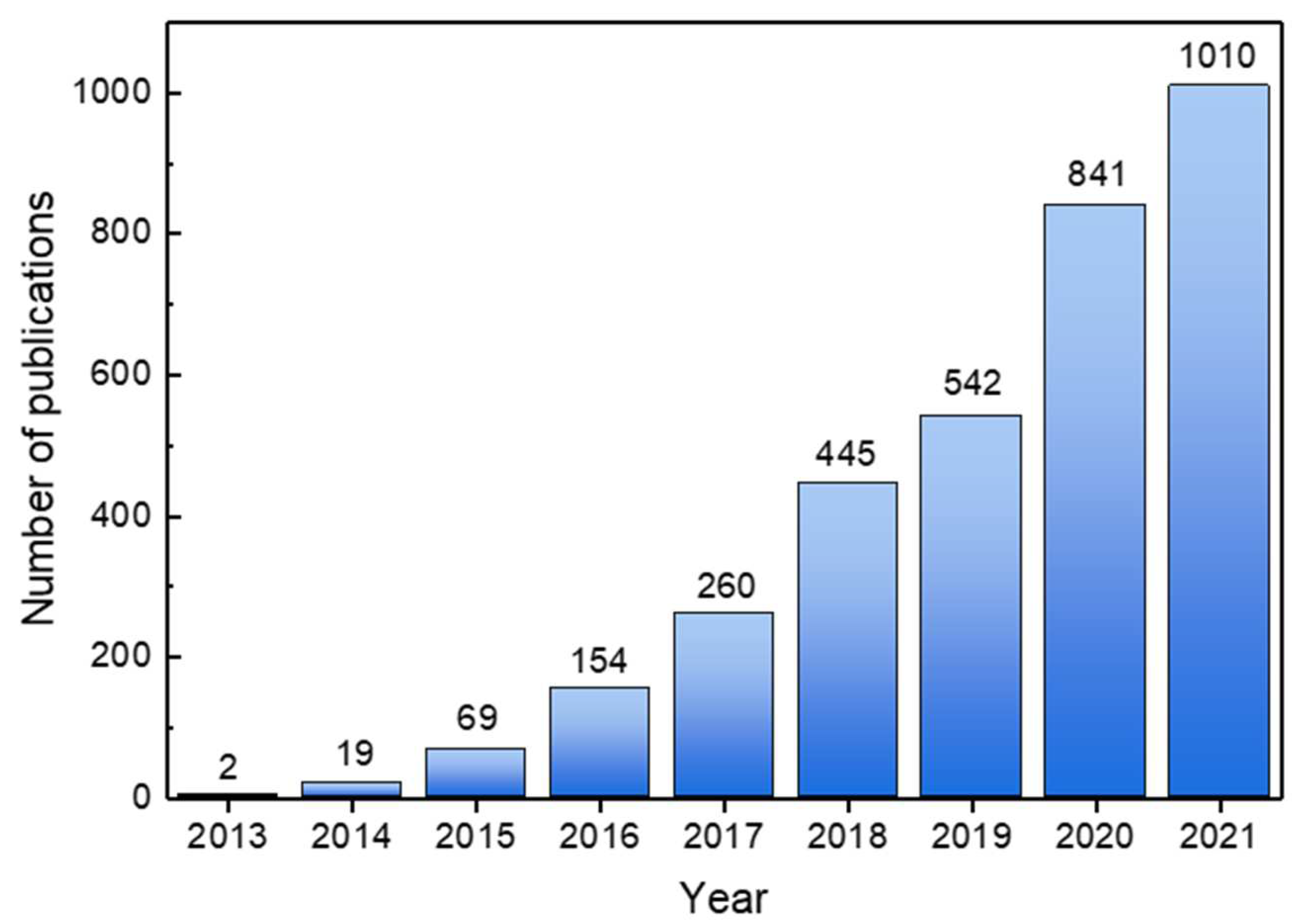
:1. Introduction
2. Visualization of Halide Segregation
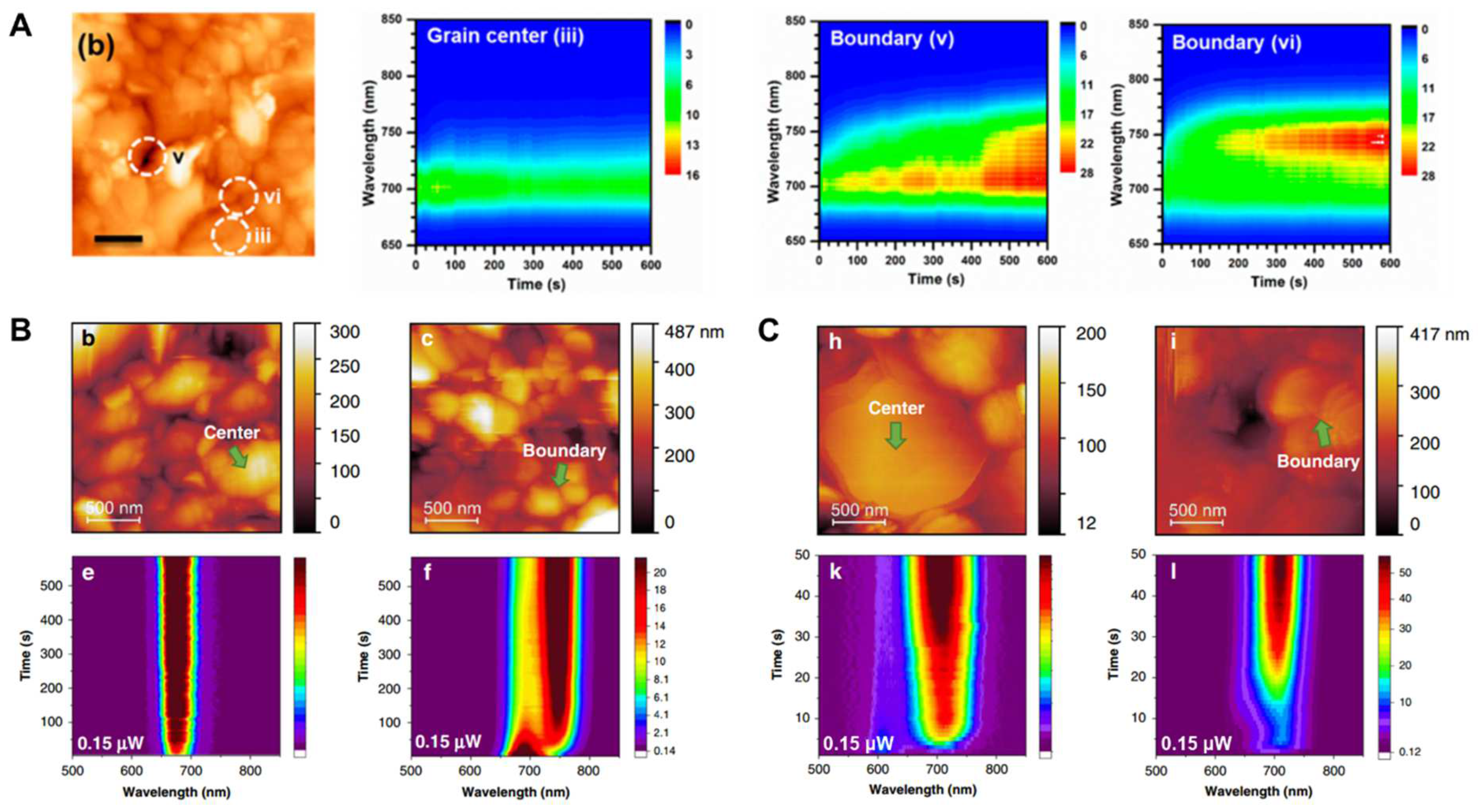
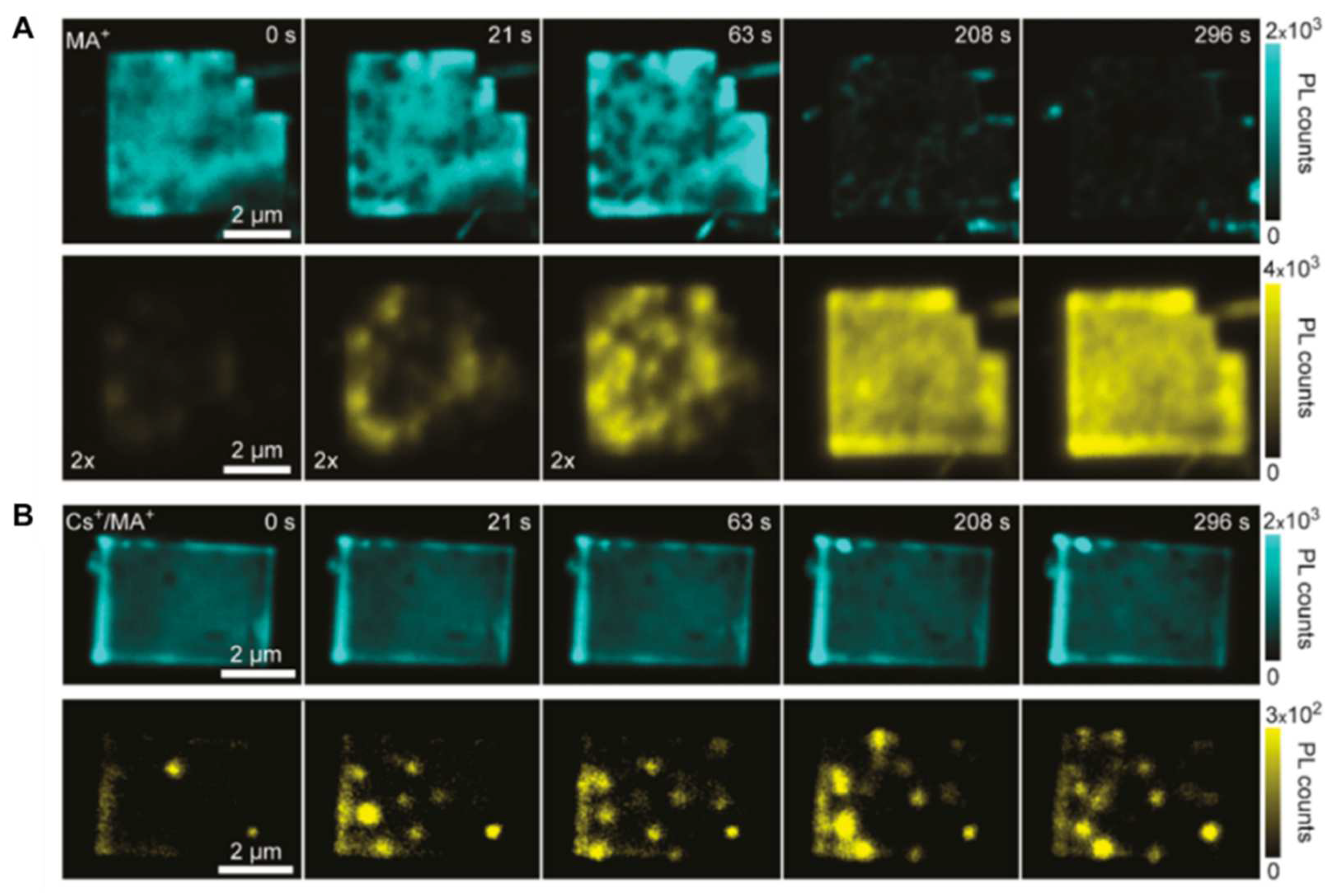
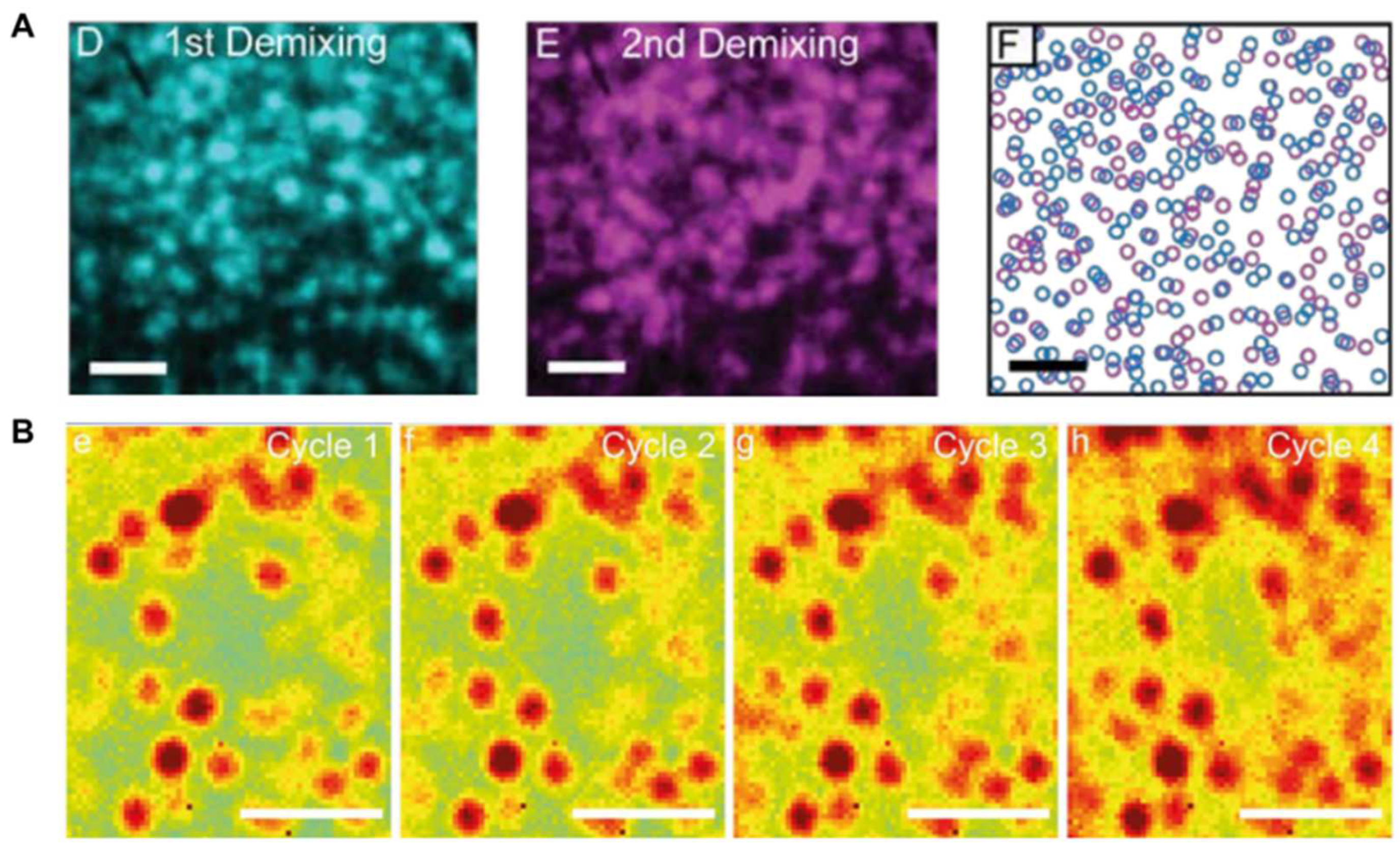
2.1. Photoluminescence Mapping
2.2. Cathodoluminescence Imaging
2.3. Transmission Electron Microscopy
2.4. Energy-Dispersive X-ray Spectroscopy

2.5. Atomic Force Microscopy
3. Mechanism of Halide Segregation in MHPs
3.1. Thermodynamic Models
3.2. Polaron/Strain Models
3.3. Carrier Gradient/Carrier Trapping Models
3.4. Redox Models
4. Summary and Outlook
Author Contributions
Funding
Institutional Review Board Statement
Informed Consent Statement
Data Availability Statement
Conflicts of Interest
References
- Kojima, A.; Teshima, K.; Shirai, Y.; Miyasaka, T. Organometal halide perovskites as visible-light sensitizers for photovoltaic cells. J. Am. Chem. Soc. 2009, 131, 6050–6051. [Google Scholar] [CrossRef] [PubMed]
- Kim, H.S.; Lee, C.R.; Im, J.H.; Lee, K.B.; Moehl, T.; Marchioro, A.; Moon, S.J.; Humphry-Baker, R.; Yum, J.H.; Moser, J.E.; et al. Lead iodide perovskite sensitized all-solid-state submicron thin film mesoscopic solar cell with efficiency exceeding 9%. Sci. Rep. 2012, 2, 591. [Google Scholar] [CrossRef] [PubMed] [Green Version]
- Lee, M.M.; Teuscher, J.; Miyasaka, T.; Murakami, T.N.; Snaith, H.J. Efficient hybrid solar cells based on meso-superstructured organometal halide perovskites. Science 2012, 338, 643–647. [Google Scholar] [CrossRef] [PubMed] [Green Version]
- Yang, W.S.; Park, B.W.; Jung, E.H.; Jeon, N.J.; Kim, Y.C.; Lee, D.U.; Shin, S.S.; Seo, J.; Kim, E.K.; Noh, J.H.; et al. Iodide management in formamidinium-lead-halide-based perovskite layers for efficient solar cells. Science 2017, 356, 1376–1379. [Google Scholar] [CrossRef] [PubMed] [Green Version]
- Jiang, Q.; Zhao, Y.; Zhang, X.; Yang, X.; Chen, Y.; Chu, Z.; Ye, Q.; Li, X.; Yin, Z.; You, J. Surface passivation of perovskite film for efficient solar cells. Nat. Photonics 2019, 13, 460–466. [Google Scholar] [CrossRef]
- Yoo, J.J.; Seo, G.; Chua, M.R.; Park, T.G.; Lu, Y.; Rotermund, F.; Kim, Y.K.; Moon, C.S.; Jeon, N.J.; Correa-Baena, J.P.; et al. Efficient perovskite solar cells via improved carrier management. Nature 2021, 590, 587–593. [Google Scholar] [CrossRef] [PubMed]
- Min, H.; Lee, D.Y.; Kim, J.; Kim, G.; Lee, K.S.; Kim, J.; Paik, M.J.; Kim, Y.K.; Kim, K.S.; Kim, M.G.; et al. Perovskite solar cells with atomically coherent interlayers on SnO2 electrodes. Nature 2021, 598, 444–450. [Google Scholar] [CrossRef]
- Park, N.G.; Zhu, K. Scalable fabrication and coating methods for perovskite solar cells and solar modules. Nat. Rev. Mater. 2020, 5, 333–350. [Google Scholar] [CrossRef]
- Bu, T.; Li, J.; Li, H.; Tian, C.; Su, J.; Tong, G.; Ono, L.K.; Wang, C.; Lin, Z.; Chai, N.; et al. Lead halide-templated crystallization of methylamine-free perovskite for efficient photovoltaic modules. Science 2021, 372, 1327–1332. [Google Scholar] [CrossRef]
- Chen, S.; Dai, X.; Xu, S.; Jiao, H.; Zhao, L.; Huang, J. Stabilizing perovskite-substrate interfaces for high-performance perovskite modules. Science 2021, 373, 902–907. [Google Scholar] [CrossRef]
- Liu, Z.; Qiu, L.; Ono, L.K.; He, S.; Hu, Z.; Jiang, M.; Tong, G.; Wu, Z.; Jiang, Y.; Son, D.-Y.; et al. A holistic approach to interface stabilization for efficient perovskite solar modules with over 2000-hour operational stability. Nat. Energy 2020, 5, 596–604. [Google Scholar] [CrossRef]
- Wang, R.; Xue, J.; Wang, K.L.; Wang, Z.K.; Luo, Y.; Fenning, D.; Xu, G.; Nuryyeva, S.; Huang, T.; Zhao, Y.; et al. Constructive molecular configurations for surface-defect passivation of perovskite photovoltaics. Science 2019, 366, 1509–1513. [Google Scholar] [CrossRef] [PubMed]
- Quan, L.N.; Rand, B.P.; Friend, R.H.; Mhaisalkar, S.G.; Lee, T.W.; Sargent, E.H. Perovskites for Next-Generation Optical Sources. Chem. Rev. 2019, 119, 7444–7477. [Google Scholar] [CrossRef] [PubMed]
- Zhao, B.; Bai, S.; Kim, V.; Lamboll, R.; Shivanna, R.; Auras, F.; Richter, J.M.; Yang, L.; Dai, L.; Alsari, M.; et al. High-efficiency perovskite–polymer bulk heterostructure light-emitting diodes. Nat. Photonics 2018, 12, 783–789. [Google Scholar] [CrossRef]
- Chu, S.; Chen, W.; Fang, Z.; Xiao, X.; Liu, Y.; Chen, J.; Huang, J.; Xiao, Z. Large-area and efficient perovskite light-emitting diodes via low-temperature blade-coating. Nat. Commun. 2021, 12, 147. [Google Scholar] [CrossRef]
- Schanze, K.S.; Kamat, P.V.; Yang, P.; Bisquert, J. Progress in Perovskite Photocatalysis. ACS Energy Lett. 2020, 5, 2602–2604. [Google Scholar] [CrossRef]
- Guan, Z.; Wu, Y.; Wang, P.; Zhang, Q.; Wang, Z.; Zheng, Z.; Liu, Y.; Dai, Y.; Whangbo, M.-H.; Huang, B. Perovskite photocatalyst CsPbBr3−xIx with a bandgap funnel structure for H2 evolution under visible light. Appl. Catal. B 2019, 245, 522–527. [Google Scholar] [CrossRef]
- Wei, H.T.; Fang, Y.J.; Mulligan, P.; Chuirazzi, W.; Fang, H.H.; Wang, C.C.; Ecker, B.R.; Gao, Y.L.; Loi, M.A.; Cao, L.; et al. Sensitive X-ray detectors made of methylammonium lead tribromide perovskite single crystals. Nat. Photonics 2016, 10, 333–339. [Google Scholar] [CrossRef]
- Tsai, H.H.; Liu, F.Z.; Shrestha, S.; Fernando, K.; Tretiak, S.; Scott, B.; Vo, D.T.; Strzalka, J.; Nie, W.Y. A sensitive and robust thin-film x-ray detector using 2D layered perovskite diodes. Sci. Adv. 2020, 6, aay0815. [Google Scholar] [CrossRef] [Green Version]
- Dong, H.; Zhang, C.; Liu, X.; Yao, J.; Zhao, Y.S. Materials chemistry and engineering in metal halide perovskite lasers. Chem. Soc. Rev. 2020, 49, 951–982. [Google Scholar] [CrossRef]
- Zhang, Q.; Shang, Q.; Su, R.; Do, T.T.H.; Xiong, Q. Halide Perovskite Semiconductor Lasers: Materials, Cavity Design, and Low Threshold. Nano Lett. 2021, 21, 1903–1914. [Google Scholar] [CrossRef] [PubMed]
- She, X.J.; Chen, C.; Divitini, G.; Zhao, B.D.; Li, Y.; Wang, J.Z.; Orri, J.F.; Cui, L.S.; Xu, W.D.; Peng, J.; et al. A solvent-based surface cleaning and passivation technique for suppressing ionic defects in high-mobility perovskite field-effect transistors. Nat. Electron. 2020, 3, 694–703. [Google Scholar] [CrossRef]
- Senanayak, S.P.; Abdi-Jalebi, M.; Kamboj, V.S.; Carey, R.; Shivanna, R.; Tian, T.; Schweicher, G.; Wang, J.; Giesbrecht, N.; Di Nuzzo, D.; et al. A general approach for hysteresis-free, operationally stable metal halide perovskite field-effect transistors. Sci. Adv. 2020, 6, eaaz4948. [Google Scholar] [CrossRef] [Green Version]
- Liu, T.; Zhao, X.; Li, J.; Liu, Z.; Liscio, F.; Milita, S.; Schroeder, B.C.; Fenwick, O. Enhanced control of self-doping in halide perovskites for improved thermoelectric performance. Nat. Commun. 2019, 10, 5750. [Google Scholar] [CrossRef] [PubMed]
- Xu, J.; Li, X.; Xiong, J.; Yuan, C.; Semin, S.; Rasing, T.; Bu, X.H. Halide Perovskites for Nonlinear Optics. Adv. Mater. 2020, 32, e1806736. [Google Scholar] [CrossRef] [PubMed]
- Privitera, A.; Righetto, M.; Cacialli, F.; Riede, M.K. Perspectives of Organic and Perovskite-Based Spintronics. Adv. Opt. Mater. 2021, 9, 2100215. [Google Scholar] [CrossRef]
- Dunlap-Shohl, W.A.; Zhou, Y.; Padture, N.P.; Mitzi, D.B. Synthetic Approaches for Halide Perovskite Thin Films. Chem. Rev. 2019, 119, 3193–3295. [Google Scholar] [CrossRef]
- Kim, J.Y.; Lee, J.W.; Jung, H.S.; Shin, H.; Park, N.G. High-Efficiency Perovskite Solar Cells. Chem. Rev. 2020, 120, 7867–7918. [Google Scholar] [CrossRef]
- Lai, M.; Obliger, A.; Lu, D.; Kley, C.S.; Bischak, C.G.; Kong, Q.; Lei, T.; Dou, L.; Ginsberg, N.S.; Limmer, D.T.; et al. Intrinsic anion diffusivity in lead halide perovskites is facilitated by a soft lattice. Proc. Natl. Acad. Sci. USA 2018, 115, 11929–11934. [Google Scholar] [CrossRef] [Green Version]
- Yuan, Y.; Huang, J. Ion Migration in Organometal Trihalide Perovskite and Its Impact on Photovoltaic Efficiency and Stability. Acc. Chem. Res. 2016, 49, 286–293. [Google Scholar] [CrossRef] [Green Version]
- Hoke, E.T.; Slotcavage, D.J.; Dohner, E.R.; Bowring, A.R.; Karunadasa, H.I.; McGehee, M.D. Reversible photo-induced trap formation in mixed-halide hybrid perovskites for photovoltaics. Chem. Sci. 2015, 6, 613–617. [Google Scholar] [CrossRef] [PubMed] [Green Version]
- Keshavarz, M.; Ottesen, M.; Wiedmann, S.; Wharmby, M.; Kuchler, R.; Yuan, H.; Debroye, E.; Steele, J.A.; Martens, J.; Hussey, N.E.; et al. Tracking Structural Phase Transitions in Lead-Halide Perovskites by Means of Thermal Expansion. Adv. Mater. 2019, 31, e1900521. [Google Scholar] [CrossRef]
- Berhe, T.A.; Su, W.N.; Chen, C.H.; Pan, C.J.; Cheng, J.H.; Chen, H.M.; Tsai, M.C.; Chen, L.Y.; Dubale, A.A.; Hwang, B.J. Organometal halide perovskite solar cells: Degradation and stability. Energy Environ. Sci. 2016, 9, 323–356. [Google Scholar] [CrossRef]
- Wei, J.; Wang, Q.; Huo, J.; Gao, F.; Gan, Z.; Zhao, Q.; Li, H. Mechanisms and Suppression of Photoinduced Degradation in Perovskite Solar Cells. Adv. Energy Mater. 2020, 11, 2002326. [Google Scholar] [CrossRef]
- Zhou, Y.; Poli, I.; Meggiolaro, D.; De Angelis, F.; Petrozza, A. Defect activity in metal halide perovskites with wide and narrow bandgap. Nat. Rev. Mater. 2021, 6, 986–1002. [Google Scholar] [CrossRef]
- Brennan, M.C.; Draguta, S.; Kamat, P.V.; Kuno, M. Light-Induced Anion Phase Segregation in Mixed Halide Perovskites. ACS Energy Lett. 2018, 3, 204–213. [Google Scholar] [CrossRef] [Green Version]
- Gualdrón-Reyes, A.F.; Yoon, S.J.; Mora-Seró, I. Recent insights for achieving mixed halide perovskites without halide segregation. Curr. Opin. Electrochem. 2018, 11, 84–90. [Google Scholar] [CrossRef]
- Brennan, M.C.; Ruth, A.; Kamat, P.V.; Kuno, M. Photoinduced Anion Segregation in Mixed Halide Perovskites. Trends Chem. 2020, 2, 282–301. [Google Scholar] [CrossRef] [Green Version]
- Knight, A.J.; Herz, L.M. Preventing phase segregation in mixed-halide perovskites: A perspective. Energy Environ. Sci. 2020, 13, 2024–2046. [Google Scholar] [CrossRef]
- Guo, Y.; Yin, X.; Que, W.; Liu, W.; Liu, H. Toward mixed-halide perovskites: Insight into photo-induced anion phase segregation. J. Mater. Chem. C 2020, 8, 14626–14644. [Google Scholar] [CrossRef]
- Wang, Y.; Quintana, X.; Kim, J.; Guan, X.; Hu, L.; Lin, C.-H.; Jones, B.T.; Chen, W.; Wen, X.; Gao, H.; et al. Phase segregation in inorganic mixed-halide perovskites: From phenomena to mechanisms. Photonics Res. 2020, 8, 402411. [Google Scholar] [CrossRef]
- Kuno, M.; Brennan, M.C. What Exactly Causes Light-Induced Halide Segregation in Mixed-Halide Perovskites? Matter 2020, 2, 21–23. [Google Scholar] [CrossRef]
- Choe, H.; Jeon, D.; Lee, S.J.; Cho, J. Mixed or Segregated: Toward Efficient and Stable Mixed Halide Perovskite-Based Devices. ACS Omega 2021, 6, 24304–24315. [Google Scholar] [CrossRef] [PubMed]
- Kamat, P.V.; Kuno, M. Halide Ion Migration in Perovskite Nanocrystals and Nanostructures. Acc. Chem. Res. 2021, 54, 520–531. [Google Scholar] [CrossRef] [PubMed]
- Kerner, R.A.; Xu, Z.; Larson, B.W.; Rand, B.P. The role of halide oxidation in perovskite halide phase separation. Joule 2021, 5, 2273–2295. [Google Scholar] [CrossRef]
- Jošt, M.; Kegelmann, L.; Korte, L.; Albrecht, S. Monolithic Perovskite Tandem Solar Cells: A Review of the Present Status and Advanced Characterization Methods Toward 30% Efficiency. Adv. Energy Mater. 2020, 10, 1904102. [Google Scholar] [CrossRef]
- deQuilettes, D.W.; Vorpahl, S.M.; Stranks, S.D.; Nagaoka, H.; Eperon, G.E.; Ziffer, M.E.; Snaith, H.J.; Ginger, D.S. Impact of microstructure on local carrier lifetime in perovskite solar cells. Science 2015, 348, 683–686. [Google Scholar] [CrossRef] [Green Version]
- deQuilettes, D.W.; Zhang, W.; Burlakov, V.M.; Graham, D.J.; Leijtens, T.; Osherov, A.; Bulovic, V.; Snaith, H.J.; Ginger, D.S.; Stranks, S.D. Photo-induced halide redistribution in organic-inorganic perovskite films. Nat. Commun. 2016, 7, 11683. [Google Scholar] [CrossRef]
- deQuilettes, D.W.; Jariwala, S.; Burke, S.; Ziffer, M.E.; Wang, J.T.; Snaith, H.J.; Ginger, D.S. Tracking Photoexcited Carriers in Hybrid Perovskite Semiconductors: Trap-Dominated Spatial Heterogeneity and Diffusion. ACS Nano 2017, 11, 11488–11496. [Google Scholar] [CrossRef]
- Yang, M.; Zeng, Y.; Li, Z.; Kim, D.H.; Jiang, C.S.; van de Lagemaat, J.; Zhu, K. Do grain boundaries dominate non-radiative recombination in CH3NH3PbI3 perovskite thin films? Phys. Chem. Chem. Phys. 2017, 19, 5043–5050. [Google Scholar] [CrossRef]
- Li, C.; Guerrero, A.; Zhong, Y.; Graser, A.; Luna, C.A.M.; Kohler, J.; Bisquert, J.; Hildner, R.; Huettner, S. Real-Time Observation of Iodide Ion Migration in Methylammonium Lead Halide Perovskites. Small 2017, 13, 1701711. [Google Scholar] [CrossRef] [PubMed]
- Li, C.; Guerrero, A.; Huettner, S.; Bisquert, J. Unravelling the role of vacancies in lead halide perovskite through electrical switching of photoluminescence. Nat. Commun. 2018, 9, 5113. [Google Scholar] [CrossRef] [PubMed] [Green Version]
- Frohna, K.; Anaya, M.; Macpherson, S.; Sung, J.; Doherty, T.A.S.; Chiang, Y.H.; Winchester, A.J.; Orr, K.W.P.; Parker, J.E.; Quinn, P.D.; et al. Nanoscale chemical heterogeneity dominates the optoelectronic response of alloyed perovskite solar cells. Nat. Nanotechnol. 2021, 17, 190–196. [Google Scholar] [CrossRef]
- Kosar, S.; Winchester, A.J.; Doherty, T.A.S.; Macpherson, S.; Petoukhoff, C.E.; Frohna, K.; Anaya, M.; Chan, N.S.; Madéo, J.; Man, M.K.L.; et al. Unraveling the varied nature and roles of defects in hybrid halide perovskites with time-resolved photoemission electron microscopy. Energy Environ. Sci. 2021, 14, 6320–6328. [Google Scholar] [CrossRef] [PubMed]
- Jariwala, S.; Sun, H.; Adhyaksa, G.W.P.; Lof, A.; Muscarella, L.A.; Ehrler, B.; Garnett, E.C.; Ginger, D.S. Local Crystal Misorientation Influences Non-radiative Recombination in Halide Perovskites. Joule 2019, 3, 3048–3060. [Google Scholar] [CrossRef] [Green Version]
- Tang, X.; van den Berg, M.; Gu, E.; Horneber, A.; Matt, G.J.; Osvet, A.; Meixner, A.J.; Zhang, D.; Brabec, C.J. Local Observation of Phase Segregation in Mixed-Halide Perovskite. Nano Lett. 2018, 18, 2172–2178. [Google Scholar] [CrossRef]
- Zhao, Y.; Miao, P.; Elia, J.; Hu, H.; Wang, X.; Heumueller, T.; Hou, Y.; Matt, G.J.; Osvet, A.; Chen, Y.T.; et al. Strain-activated light-induced halide segregation in mixed-halide perovskite solids. Nat. Commun. 2020, 11, 6328. [Google Scholar] [CrossRef]
- Yin, X.; Guo, Y.; Liu, J.; Que, W.; Ma, F.; Xu, K. Photoinduced Phase Segregation Leading to Evident Open-Circuit Voltage Loss in Efficient Inorganic CsPbIBr2 Solar Cells. J. Phys. Chem. Lett. 2020, 11, 7035–7041. [Google Scholar] [CrossRef]
- Tiede, D.O.; Calvo, M.E.; Galisteo-Lopez, J.F.; Miguez, H. Local Rearrangement of the Iodide Defect Structure Determines the Phase Segregation Effect in Mixed-Halide Perovskites. J. Phys. Chem. Lett. 2020, 11, 4911–4916. [Google Scholar] [CrossRef]
- Yoon, S.J.; Kuno, M.; Kamat, P.V. Shift Happens. How Halide Ion Defects Influence Photoinduced Segregation in Mixed Halide Perovskites. ACS Energy Lett. 2017, 2, 1507–1514. [Google Scholar] [CrossRef] [Green Version]
- Barker, A.J.; Sadhanala, A.; Deschler, F.; Gandini, M.; Senanayak, S.P.; Pearce, P.M.; Mosconi, E.; Pearson, A.J.; Wu, Y.; Srimath Kandada, A.R.; et al. Defect-Assisted Photoinduced Halide Segregation in Mixed-Halide Perovskite Thin Films. ACS Energy Lett. 2017, 2, 1416–1424. [Google Scholar] [CrossRef]
- Belisle, R.A.; Bush, K.A.; Bertoluzzi, L.; Gold-Parker, A.; Toney, M.F.; McGehee, M.D. Impact of Surfaces on Photoinduced Halide Segregation in Mixed-Halide Perovskites. ACS Energy Lett. 2018, 3, 2694–2700. [Google Scholar] [CrossRef]
- Knight, A.J.; Wright, A.D.; Patel, J.B.; McMeekin, D.P.; Snaith, H.J.; Johnston, M.B.; Herz, L.M. Electronic Traps and Phase Segregation in Lead Mixed-Halide Perovskite. ACS Energy Lett. 2019, 4, 75–84. [Google Scholar] [CrossRef]
- Knight, A.J.; Patel, J.B.; Snaith, H.J.; Johnston, M.B.; Herz, L.M. Trap States, Electric Fields, and Phase Segregation in Mixed-Halide Perovskite Photovoltaic Devices. Adv. Energy Mater. 2020, 10, 1903488. [Google Scholar] [CrossRef]
- Motti, S.G.; Meggiolaro, D.; Barker, A.J.; Mosconi, E.; Perini, C.A.R.; Ball, J.M.; Gandini, M.; Kim, M.; De Angelis, F.; Petrozza, A. Controlling competing photochemical reactions stabilizes perovskite solar cells. Nat. Photonics 2019, 13, 532–539. [Google Scholar] [CrossRef]
- Ruth, A.; Brennan, M.C.; Draguta, S.; Morozov, Y.V.; Zhukovskyi, M.; Janko, B.; Zapol, P.; Kuno, M. Vacancy-Mediated Anion Photosegregation Kinetics in Mixed Halide Hybrid Perovskites: Coupled Kinetic Monte Carlo and Optical Measurements. ACS Energy Lett. 2018, 3, 2321–2328. [Google Scholar] [CrossRef]
- Datta, K.; van Gorkom, B.T.; Chen, Z.; Dyson, M.J.; van der Pol, T.P.A.; Meskers, S.C.J.; Tao, S.; Bobbert, P.A.; Wienk, M.M.; Janssen, R.A.J. Effect of Light-Induced Halide Segregation on the Performance of Mixed-Halide Perovskite Solar Cells. ACS Appl. Energy Mater. 2021, 4, 6650–6658. [Google Scholar] [CrossRef]
- Doherty, T.A.S.; Winchester, A.J.; Macpherson, S.; Johnstone, D.N.; Pareek, V.; Tennyson, E.M.; Kosar, S.; Kosasih, F.U.; Anaya, M.; Abdi-Jalebi, M.; et al. Performance-limiting nanoscale trap clusters at grain junctions in halide perovskites. Nature 2020, 580, 360–366. [Google Scholar] [CrossRef]
- Park, J.-S.; Calbo, J.; Jung, Y.-K.; Whalley, L.D.; Walsh, A. Accumulation of Deep Traps at Grain Boundaries in Halide Perovskites. ACS Energy Lett. 2019, 4, 1321–1327. [Google Scholar] [CrossRef]
- Tennyson, E.M.; Doherty, T.A.S.; Stranks, S.D. Heterogeneity at multiple length scales in halide perovskite semiconductors. Nat. Rev. Mater. 2019, 4, 573–587. [Google Scholar] [CrossRef]
- Duong, T.; Mulmudi, H.K.; Wu, Y.; Fu, X.; Shen, H.; Peng, J.; Wu, N.; Nguyen, H.T.; Macdonald, D.; Lockrey, M.; et al. Light and Electrically Induced Phase Segregation and Its Impact on the Stability of Quadruple Cation High Bandgap Perovskite Solar Cells. ACS Appl. Mater. Interfaces 2017, 9, 26859–26866. [Google Scholar] [CrossRef] [PubMed]
- Suchan, K.; Merdasa, A.; Rehermann, C.; Unger, E.L.; Scheblykin, I.G. Complex evolution of photoluminescence during phase segregation of MAPb(I1−xBrx)3 mixed halide perovskite. J. Lumin. 2020, 221, 117073. [Google Scholar] [CrossRef]
- Zhong, Y.; Luna, C.A.M.; Hildner, R.; Li, C.; Huettner, S. In situ investigation of light soaking in organolead halide perovskite films. APL Mater. 2019, 7, 041114. [Google Scholar] [CrossRef] [Green Version]
- Vicente, J.R.; Chen, J. Phase Segregation and Photothermal Remixing of Mixed-Halide Lead Perovskites. J. Phys. Chem. Lett. 2020, 11, 1802–1807. [Google Scholar] [CrossRef] [PubMed]
- Bischak, C.G.; Wong, A.B.; Lin, E.; Limmer, D.T.; Yang, P.; Ginsberg, N.S. Tunable Polaron Distortions Control the Extent of Halide Demixing in Lead Halide Perovskites. J. Phys. Chem. Lett. 2018, 9, 3998–4005. [Google Scholar] [CrossRef] [Green Version]
- Mao, W.; Hall, C.R.; Chesman, A.S.R.; Forsyth, C.; Cheng, Y.B.; Duffy, N.W.; Smith, T.A.; Bach, U. Visualizing Phase Segregation in Mixed-Halide Perovskite Single Crystals. Angew. Chem. Int. Ed. 2019, 58, 2893–2898. [Google Scholar] [CrossRef]
- Bischak, C.G.; Hetherington, C.L.; Wu, H.; Aloni, S.; Ogletree, D.F.; Limmer, D.T.; Ginsberg, N.S. Origin of Reversible Photoinduced Phase Separation in Hybrid Perovskites. Nano Lett. 2017, 17, 1028–1033. [Google Scholar] [CrossRef] [Green Version]
- Zhou, W.; Zhao, Y.; Zhou, X.; Fu, R.; Li, Q.; Zhao, Y.; Liu, K.; Yu, D.; Zhao, Q. Light-Independent Ionic Transport in Inorganic Perovskite and Ultrastable Cs-Based Perovskite Solar Cells. J. Phys. Chem. Lett. 2017, 8, 4122–4128. [Google Scholar] [CrossRef]
- Rehman, W.; McMeekin, D.P.; Patel, J.B.; Milot, R.L.; Johnston, M.B.; Snaith, H.J.; Herz, L.M. Photovoltaic mixed-cation lead mixed-halide perovskites: Links between crystallinity, photo-stability and electronic properties. Energy Environ. Sci. 2017, 10, 361–369. [Google Scholar] [CrossRef] [Green Version]
- Huang, J.; Xu, P.; Liu, J.; You, X.Z. Sequential Introduction of Cations Deriving Large-Grain CsxFA1−xPbI3 Thin Film for Planar Hybrid Solar Cells: Insight into Phase-Segregation and Thermal-Healing Behavior. Small 2017, 13, 1603225. [Google Scholar] [CrossRef]
- Dang, H.X.; Wang, K.; Ghasemi, M.; Tang, M.-C.; De Bastiani, M.; Aydin, E.; Dauzon, E.; Barrit, D.; Peng, J.; Smilgies, D.-M.; et al. Multi-cation Synergy Suppresses Phase Segregation in Mixed-Halide Perovskites. Joule 2019, 3, 1746–1764. [Google Scholar] [CrossRef]
- Beal, R.E.; Hagström, N.Z.; Barrier, J.; Gold-Parker, A.; Prasanna, R.; Bush, K.A.; Passarello, D.; Schelhas, L.T.; Brüning, K.; Tassone, C.J.; et al. Structural Origins of Light-Induced Phase Segregation in Organic-Inorganic Halide Perovskite Photovoltaic Materials. Matter 2020, 2, 207–219. [Google Scholar] [CrossRef] [Green Version]
- Mathew, P.S.; Samu, G.F.; Janáky, C.; Kamat, P.V. Iodine (I) Expulsion at Photoirradiated Mixed Halide Perovskite Interface. Should I Stay or Should I Go? ACS Energy Lett. 2020, 5, 1872–1880. [Google Scholar] [CrossRef]
- Zhang, Q.; Su, R.; Liu, X.; Xing, J.; Sum, T.C.; Xiong, Q. High-Quality Whispering-Gallery-Mode Lasing from Cesium Lead Halide Perovskite Nanoplatelets. Adv. Funct. Mater. 2016, 26, 6238–6245. [Google Scholar] [CrossRef]
- Dar, M.I.; Jacopin, G.; Hezam, M.; Arora, N.; Zakeeruddin, S.M.; Deveaud, B.; Nazeeruddin, M.K.; Grätzel, M. Asymmetric Cathodoluminescence Emission in CH3NH3PbI3–xBrx Perovskite Single Crystals. ACS Photonics 2016, 3, 947–952. [Google Scholar] [CrossRef]
- Chen, W.; Mao, W.; Bach, U.; Jia, B.; Wen, X. Tracking Dynamic Phase Segregation in Mixed-Halide Perovskite Single Crystals under Two-Photon Scanning Laser Illumination. Small Methods 2019, 3, 1900273. [Google Scholar] [CrossRef]
- Stavrakas, C.; Zhumekenov, A.A.; Brenes, R.; Abdi-Jalebi, M.; Bulovic, V.; Bakr, O.M.; Barnard, E.S.; Stranks, S.D. Probing buried recombination pathways in perovskite structures using 3D photoluminescence tomography. Energy Environ. Sci. 2018, 11, 2846–2852. [Google Scholar] [CrossRef] [Green Version]
- Bischak, C.G.; Sanehira, E.M.; Precht, J.T.; Luther, J.M.; Ginsberg, N.S. Heterogeneous Charge Carrier Dynamics in Organic-Inorganic Hybrid Materials: Nanoscale Lateral and Depth-Dependent Variation of Recombination Rates in Methylammonium Lead Halide Perovskite Thin Films. Nano Lett. 2015, 15, 4799–4807. [Google Scholar] [CrossRef]
- Xiao, C.; Li, Z.; Guthrey, H.; Moseley, J.; Yang, Y.; Wozny, S.; Moutinho, H.; To, B.; Berry, J.J.; Gorman, B.; et al. Mechanisms of Electron-Beam-Induced Damage in Perovskite Thin Films Revealed by Cathodoluminescence Spectroscopy. J. Phys. Chem. C 2015, 119, 26904–26911. [Google Scholar] [CrossRef]
- Stranks, S.D. Multimodal microscopy characterization of halide perovskite semiconductors: Revealing a new world (dis)order. Matter 2021, 4, 3852–3866. [Google Scholar] [CrossRef]
- Li, W.; Rothmann, M.U.; Liu, A.; Wang, Z.; Zhang, Y.; Pascoe, A.R.; Lu, J.; Jiang, L.; Chen, Y.; Huang, F.; et al. Phase Segregation Enhanced Ion Movement in Efficient Inorganic CsPbIBr2 Solar Cells. Adv. Energy Mater. 2017, 7, 1700946. [Google Scholar] [CrossRef]
- Kumar, V.; Nisika; Kumar, M. Temporal-spatial-energy resolved advance multidimensional techniques to probe photovoltaic materials from atomistic viewpoint for next-generation energy solutions. Energy Environ. Sci. 2021, 14, 4760–4802. [Google Scholar] [CrossRef]
- Hidalgo, J.; Castro-Méndez, A.F.; Correa-Baena, J.P. Imaging and Mapping Characterization Tools for Perovskite Solar Cells. Adv. Energy Mater. 2019, 9, 1900444. [Google Scholar] [CrossRef]
- Funk, H.; Shargaieva, O.; Eljarrat, A.; Unger, E.L.; Koch, C.T.; Abou-Ras, D. In Situ TEM Monitoring of Phase-Segregation in Inorganic Mixed Halide Perovskite. J. Phys. Chem. Lett. 2020, 11, 4945–4950. [Google Scholar] [CrossRef]
- Notthoff, C.; Winterer, M.; Beckel, A.; Geller, M.; Heindl, J. Spatial high resolution energy dispersive X-ray spectroscopy on thin lamellas. Ultramicroscopy 2013, 129, 30–35. [Google Scholar] [CrossRef]
- Hentz, O.; Zhao, Z.; Gradecak, S. Impacts of Ion Segregation on Local Optical Properties in Mixed Halide Perovskite Films. Nano Lett. 2016, 16, 1485–1490. [Google Scholar] [CrossRef]
- Frolova, L.A.; Luchkin, S.Y.; Lekina, Y.; Gutsev, L.G.; Tsarev, S.A.; Zhidkov, I.S.; Kurmaev, E.Z.; Shen, Z.X.; Stevenson, K.J.; Aldoshin, S.M.; et al. Reversible Pb2+/Pb0 and I−/I3− Redox Chemistry Drives the Light-Induced Phase Segregation in All-Inorganic Mixed Halide Perovskites. Adv. Energy Mater. 2021, 11, 2002934. [Google Scholar] [CrossRef]
- Melitz, W.; Shen, J.; Kummel, A.C.; Lee, S. Kelvin probe force microscopy and its application. Surf. Sci. Rep. 2011, 66, 1–27. [Google Scholar] [CrossRef]
- Gomez, A.; Sanchez, S.; Campoy-Quiles, M.; Abate, A. Topological distribution of reversible and non-reversible degradation in perovskite solar cells. Nano Energy 2018, 45, 94–100. [Google Scholar] [CrossRef] [Green Version]
- Samu, G.F.; Balog, A.; De Angelis, F.; Meggiolaro, D.; Kamat, P.V.; Janaky, C. Electrochemical Hole Injection Selectively Expels Iodide from Mixed Halide Perovskite Films. J. Am. Chem. Soc. 2019, 141, 10812–10820. [Google Scholar] [CrossRef] [Green Version]
- Brivio, F.; Caetano, C.; Walsh, A. Thermodynamic Origin of Photoinstability in the CH3NH3Pb(I1−xBrx)3 Hybrid Halide Perovskite Alloy. J. Phys. Chem. Lett. 2016, 7, 1083–1087. [Google Scholar] [CrossRef] [PubMed] [Green Version]
- Draguta, S.; Sharia, O.; Yoon, S.J.; Brennan, M.C.; Morozov, Y.V.; Manser, J.S.; Kamat, P.V.; Schneider, W.F.; Kuno, M. Rationalizing the light-induced phase separation of mixed halide organic-inorganic perovskites. Nat. Commun. 2017, 8, 200. [Google Scholar] [CrossRef] [PubMed] [Green Version]
- Pavlovetc, I.M.; Ruth, A.; Gushchina, I.; Ngo, L.; Zhang, S.; Zhang, Z.; Kuno, M. Distinguishing Models for Mixed Halide Lead Perovskite Photosegregation via Terminal Halide Stoichiometry. ACS Energy Lett. 2021, 6, 2064–2071. [Google Scholar] [CrossRef]
- Chen, Z.; Brocks, G.; Tao, S.; Bobbert, P.A. Unified theory for light-induced halide segregation in mixed halide perovskites. Nat. Commun. 2021, 12, 2687. [Google Scholar] [CrossRef] [PubMed]
- Wagemaker, M.; Singh, D.P.; Borghols, W.J.; Lafont, U.; Haverkate, L.; Peterson, V.K.; Mulder, F.M. Dynamic solubility limits in nanosized olivine LiFePO4. J. Am. Chem. Soc. 2011, 133, 10222–10228. [Google Scholar] [CrossRef] [PubMed]
- Bai, P.; Cogswell, D.A.; Bazant, M.Z. Suppression of phase separation in LiFePO4 nanoparticles during battery discharge. Nano Lett. 2011, 11, 4890–4896. [Google Scholar] [CrossRef] [Green Version]
- Zhu, C.; Mu, X.; Popovic, J.; Weichert, K.; van Aken, P.A.; Yu, Y.; Maier, J. Lithium potential variations for metastable materials: Case study of nanocrystalline and amorphous LiFePO4. Nano Lett. 2014, 14, 5342–5349. [Google Scholar] [CrossRef]
- Wang, Y.-R.; Yeong Kim, G.; Kotomin, E.; Moia, D.; Maier, J. Photo de-mixing in mixed halide perovskites: The roles of ions and electrons. J. Phys. Energy 2022. [Google Scholar] [CrossRef]
- Wang, X.; Ling, Y.; Lian, X.; Xin, Y.; Dhungana, K.B.; Perez-Orive, F.; Knox, J.; Chen, Z.; Zhou, Y.; Beery, D.; et al. Suppressed phase separation of mixed-halide perovskites confined in endotaxial matrices. Nat. Commun. 2019, 10, 695. [Google Scholar] [CrossRef]
- Babbe, F.; Masquelier, E.; Zheng, Z.; Sutter-Fella, C.M. Flash Formation of I-Rich Clusters during Multistage Halide Segregation Studied in MAPbI1.5Br1.5. J. Phys. Chem. C 2020, 124, 24608–24615. [Google Scholar] [CrossRef]
- Mao, W.; Hall, C.R.; Bernardi, S.; Cheng, Y.B.; Widmer-Cooper, A.; Smith, T.A.; Bach, U. Light-induced reversal of ion segregation in mixed-halide perovskites. Nat. Mater. 2021, 20, 55–61. [Google Scholar] [CrossRef] [PubMed]
- Guo, Y.; Yin, X.; Liu, D.; Liu, J.; Zhang, C.; Xie, H.; Yang, Y.; Que, W. Photoinduced Self-healing of Halide Segregation in Mixed-halide Perovskites. ACS Energy Lett. 2021, 6, 2502–2511. [Google Scholar] [CrossRef]
- Cho, J.; Kamat, P.V. Photoinduced Phase Segregation in Mixed Halide Perovskites: Thermodynamic and Kinetic Aspects of Cl–Br Segregation. Adv. Opt. Mater. 2020, 9, 2001440. [Google Scholar] [CrossRef]
- Elmelund, T.; Seger, B.; Kuno, M.; Kamat, P.V. How Interplay between Photo and Thermal Activation Dictates Halide Ion Segregation in Mixed Halide Perovskites. ACS Energy Lett. 2019, 5, 56–63. [Google Scholar] [CrossRef]
- van de Goor, T.W.J.; Liu, Y.; Feldmann, S.; Bourelle, S.A.; Neumann, T.; Winkler, T.; Kelly, N.D.; Liu, C.; Jones, M.A.; Emge, S.P.; et al. Impact of Orientational Glass Formation and Local Strain on Photo-Induced Halide Segregation in Hybrid Metal-Halide Perovskites. J. Phys. Chem. C 2021, 125, 15025–15034. [Google Scholar] [CrossRef]
- DuBose, J.T.; Kamat, P.V. TiO2-Assisted Halide Ion Segregation in Mixed Halide Perovskite Films. J. Am. Chem. Soc. 2020, 142, 5362–5370. [Google Scholar] [CrossRef]
- Al-Ashouri, A.; Kohnen, E.; Li, B.; Magomedov, A.; Hempel, H.; Caprioglio, P.; Marquez, J.A.; Morales Vilches, A.B.; Kasparavicius, E.; Smith, J.A.; et al. Monolithic perovskite/silicon tandem solar cell with >29% efficiency by enhanced hole extraction. Science 2020, 370, 1300–1309. [Google Scholar] [CrossRef]
- Cho, J.; DuBose, J.T.; Mathew, P.S.; Kamat, P.V. Electrochemically induced iodine migration in mixed halide perovskites: Suppression through chloride insertion. Chem. Commun. 2021, 57, 235–238. [Google Scholar] [CrossRef]
- Shi, T.; Yin, W.-J.; Hong, F.; Zhu, K.; Yan, Y. Unipolar self-doping behavior in perovskite CH3NH3PbBr3. Appl. Phys. Lett. 2015, 106, 103902. [Google Scholar] [CrossRef]
- Kim, G.Y.; Senocrate, A.; Yang, T.Y.; Gregori, G.; Gratzel, M.; Maier, J. Large tunable photoeffect on ion conduction in halide perovskites and implications for photodecomposition. Nat. Mater. 2018, 17, 445–449. [Google Scholar] [CrossRef]
- Beal, R.E.; Slotcavage, D.J.; Leijtens, T.; Bowring, A.R.; Belisle, R.A.; Nguyen, W.H.; Burkhard, G.F.; Hoke, E.T.; McGehee, M.D. Cesium Lead Halide Perovskites with Improved Stability for Tandem Solar Cells. J. Phys. Chem. Lett. 2016, 7, 746–751. [Google Scholar] [CrossRef]
- Xu, J.; Boyd, C.C.; Yu, Z.J.; Palmstrom, A.F.; Witter, D.J.; Larson, B.W.; France, R.M.; Werner, J.; Harvey, S.P.; Wolf, E.J.; et al. Triple-halide wide-band gap perovskites with suppressed phase segregation for efficient tandems. Science 2020, 367, 1097–1104. [Google Scholar] [CrossRef]
- Knight, A.J.; Borchert, J.; Oliver, R.D.J.; Patel, J.B.; Radaelli, P.G.; Snaith, H.J.; Johnston, M.B.; Herz, L.M. Halide Segregation in Mixed-Halide Perovskites: Influence of A-Site Cations. ACS Energy Lett. 2021, 6, 799–808. [Google Scholar] [CrossRef]
- Elmelund, T.; Scheidt, R.A.; Seger, B.; Kamat, P.V. Bidirectional Halide Ion Exchange in Paired Lead Halide Perovskite Films with Thermal Activation. ACS Energy Lett. 2019, 4, 1961–1969. [Google Scholar] [CrossRef]


Publisher’s Note: MDPI stays neutral with regard to jurisdictional claims in published maps and institutional affiliations. |
© 2022 by the authors. Licensee MDPI, Basel, Switzerland. This article is an open access article distributed under the terms and conditions of the Creative Commons Attribution (CC BY) license (https://creativecommons.org/licenses/by/4.0/).
Share and Cite
Tian, L.; Xue, J.; Wang, R. Halide Segregation in Mixed Halide Perovskites: Visualization and Mechanisms. Electronics 2022, 11, 700. https://doi.org/10.3390/electronics11050700
Tian L, Xue J, Wang R. Halide Segregation in Mixed Halide Perovskites: Visualization and Mechanisms. Electronics. 2022; 11(5):700. https://doi.org/10.3390/electronics11050700
Chicago/Turabian StyleTian, Liuwen, Jingjing Xue, and Rui Wang. 2022. "Halide Segregation in Mixed Halide Perovskites: Visualization and Mechanisms" Electronics 11, no. 5: 700. https://doi.org/10.3390/electronics11050700