Review

Low-Dimensional Layered Light-Sensitive Memristive Structures for Energy-Efficient Machine Vision

Institute of Microelectronics Technology of the Russian Academy of Sciences, 6, Academician Ossipyan Str., 142432 Chernogolovka, Russia
Electronics 2022, 11(4), 619; https://doi.org/10.3390/electronics11040619
Submission received: 14 January 2022 / Revised: 5 February 2022 / Accepted: 8 February 2022 / Published: 17 February 2022

Abstract

:
Layered two-dimensional (2D) and quasi-zero-dimensional (0D) materials effectively absorb radiation in the wide ultraviolet, visible, infrared, and terahertz ranges. Photomemristive structures made of such low-dimensional materials are of great interest for creating optoelectronic platforms for energy-efficient storage and processing of data and optical signals in real time. Here, photosensor and memristor structures based on graphene, graphene oxide, bismuth oxyselenide, and transition metal dichalcogenides are reviewed from the point of view of application in broadband image recognition in artificial intelligence systems for autonomous unmanned vehicles, as well as the compatibility of the formation of layered neuromorphic structures with CMOS technology.

1. Introduction

In recent years, there has been an increased interest in the creation of optoelectronic devices based on photomemristors capable of energy-saving storage and processing of signals, such as neurons and synapses in biological systems [1]. The need to improve the speed and energy efficiency of big data processing is especially acute in systems such as artificial intelligence (AI) in autopilot and autonomous unmanned vehicles. In 2021, Elon Musk presented the development of the D1 Dojo processor for the AI of the Tesla autopilot, designed to work in neural networks for pattern recognition [2]. The D1 Dojo is manufactured using 7 nm complementary metal-oxide semiconductor (CMOS) technology, has an area of 645 mm2, and contains 50 billion transistors (5 × 10¹⁰/mm2 ~ 4 × 109 cm2). For comparison, the density of conventionally computational and memory elements in the human brain is −1011 (neurons) and 1015 (synapses), respectively. A computer with a variable set D1 (Figure 1), built on the basis of 3000 such chips, would perform 1018 operations per second (1.1 EFLOPS) and consume 1.2 MW (a board of 25 chips with heat removal up to 15 kW consumes ~10 kW) [2].
This development can be compared with the K Computer of the Japanese corporation Fujitsu (2017), one of the most powerful supercomputers in the world. When simulating the work of 1% of human brain neurons, the K Computer performed 1016 operations per second (10 PFLOPS) and consumed ~10 MW. The human brain (100% neurons) consumes, as is known, about 10–20 watts. Moreover, to simulate 1 s of brain work, the supercomputer needed ~40 min. The performance of the Dojo computer is two orders of magnitude higher, but the energy consumption for autonomous operation of the autopilot remains too high. For comparison, the capacity of all power plants of the UES of Russia, including thermal, hydro, nuclear, solar, and wind power plants, as of 01.12.2021 amounted to 247,913.51 MW [3].
The low speed and energy efficiency of big data processing in digital systems is associated with the physical separation of the memory and processor (Figure 2), which causes traffic problems and limits the efficiency of information processing and the performance of computing systems.
The so-called “in-memory computing” can improve the energy efficiency of computations using memristor circuits similar to biological neural networks [4,5,6,7,8,9]. Significant research progress has been made in improving the performance of memristive devices based on 2D layered materials [10,11,12]. Two-dimensional layered materials have unique physical properties and open up great opportunities for applications in neuromorphic computing. However, to solve the problem of time delay in processing the detected signal, new approaches are needed to create photoelectronic components of AI visual systems. One such approach is “photodetecting and computing in-memory”. The development of AI systems for automatic control (piloting) of machines in an autonomous mode requires the development of a fundamentally new element base of sensor and computing devices that allow detecting and processing information in real time. Memristor structures made of photosensitive low-dimensional layered materials [13,14,15,16], which effectively absorb radiation in the ultraviolet, visible, and infrared ranges [17,18,19], can be used as an optoelectronic platform embedded in CMOS technology for fast and energy-efficient neuromorphic processing of an optical signal and pattern recognition.

2. Photomemristor

A photomemristor made from MoS2 crystals was demonstrated in 2016 [15]. Polarization of the memristor in an electric field upon excitation by light led to multilevel switching. The faster polarization process of the photomemristor in comparison with the transport of ions and the fast optical access make it possible to detect and quickly process signals in the memory.
Figure 3 shows the switching diagrams of the MoS2 photomemristor by electrical and optical pulses. The memristor, polarized at different voltages, shows eight different states that can be read electrically under optical excitation. The photomemristor provides fast multi-level non-linear dynamic operation and can be used for image detection and processing.
A photomemristor has also been demonstrated based on two-dimensional materials graphene (G) and graphene oxide (GO) [20]. It has been shown that the photocatalytic oxidation of graphene with ZnO nanoparticles creates self-assembling photosensitive G/GO heterostructures exhibiting photomemristive states. Oxygen groups released during the photodecomposition of water molecules on nanoparticles in ultraviolet light oxidize graphene, locally forming G/GO heterojunctions with a density of up to 1012/cm2. G/GO nanostructures have nonlinear current–voltage characteristics and switch resistance in an electric field upon photoexcitation, providing four resistive states at room temperature. Photocatalytic oxidation of graphene with ZnO nanoparticles makes it possible to form high-density photomemristors due to the process of the self-organization of G/GO structures, which can be used to create non-volatile ultrahigh-capacity photomemory.
Figure 4 shows a diagram of a G/GO photomemristor matrix, formed by photocatalytic oxidation in the regions near ZnO nanoparticles and a diagram of the switching of their resistive states under electrical and optical excitation. Four memristive states with an on/off current ratio of ~ 10 are well controlled in an electric field in the dark and in the light. G/GO photomemristors are promising for multi-level non-volatile ultrahigh-capacity memory that can be implemented using photocatalytic oxidation compatible with CMOS technology.

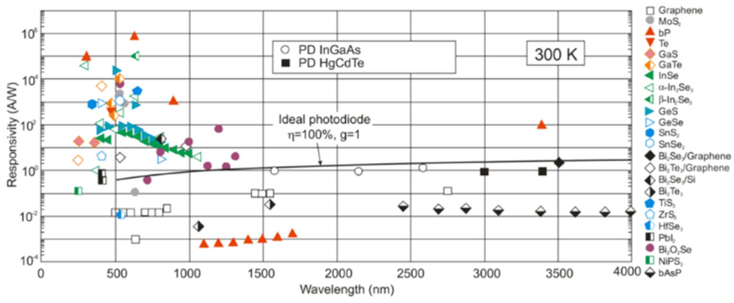
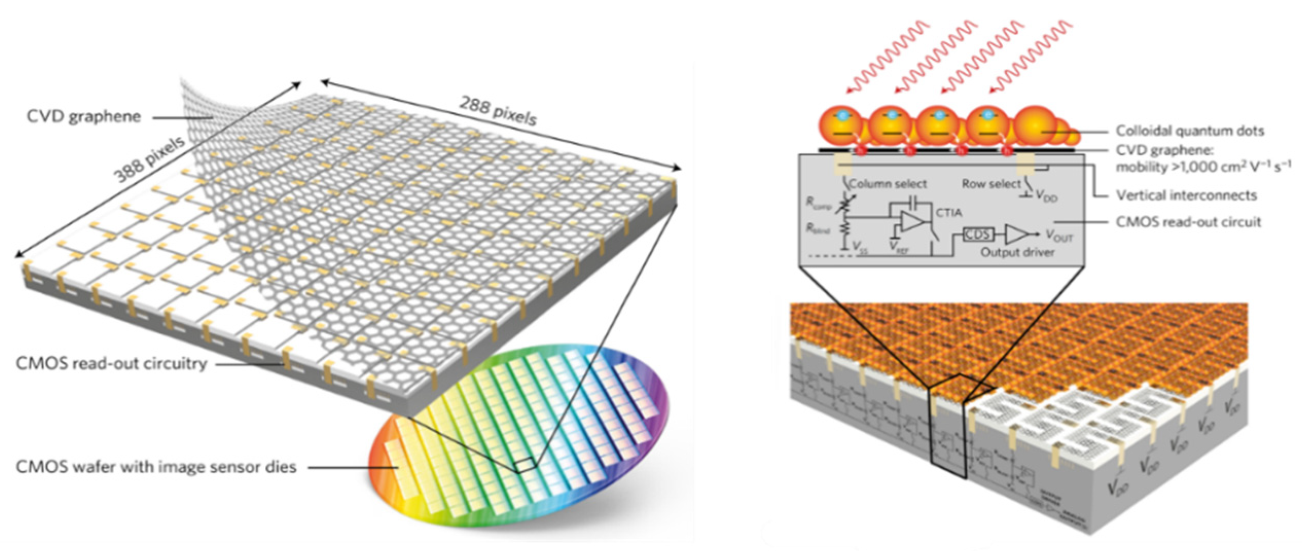
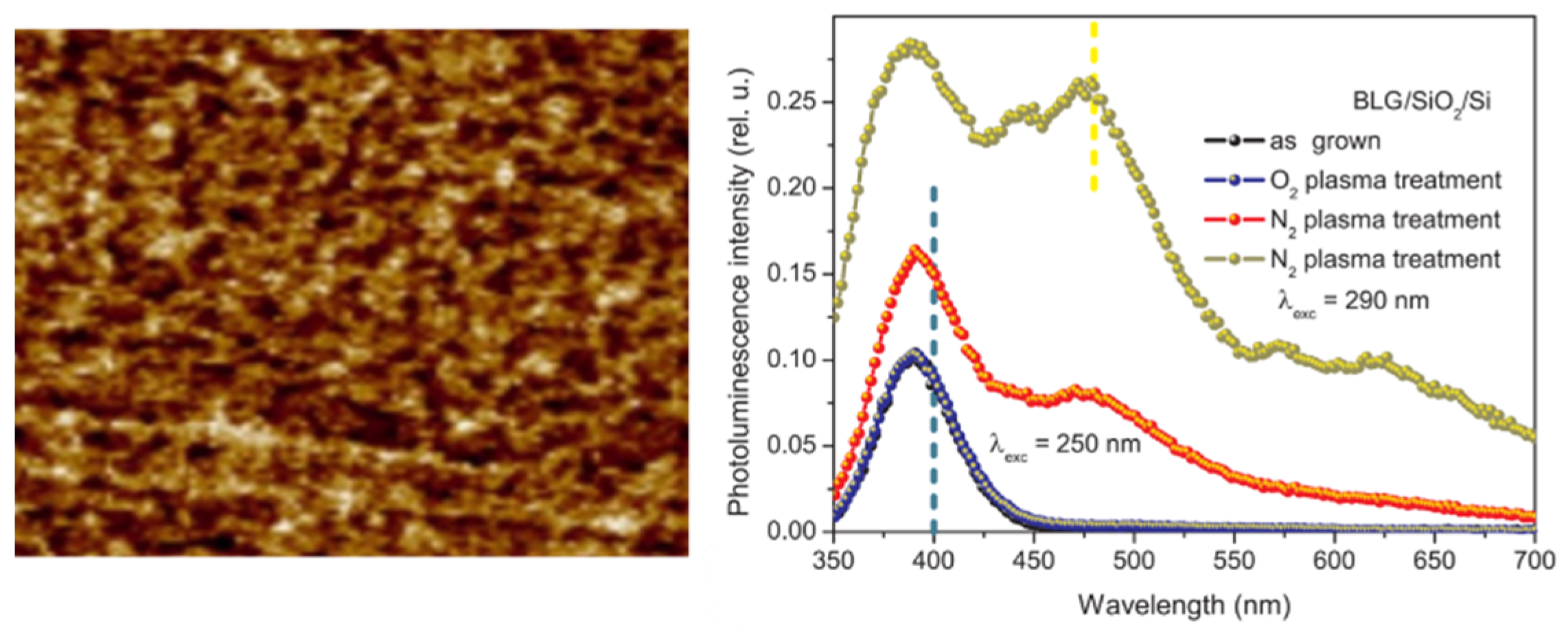
3. Photosensitive 2D Crystals and Their Embedding in CMOS Technology

Two-dimensional crystals have great potential to operate in a wide spectral range from UV to THz [21,22,23,24,25,26]. Most of them cover the visible and short-wave infrared range (Figure 5).
The uniqueness of the atomic surface of 2D materials without dangling bonds allows crystals to be embedded in CMOS technology without introducing structural defects, which makes it possible to produce high-quality functional integrated circuits for broadband detection.
CMOS-integrated circuits, which are at the heart of the microelectronics technological revolution, enable the creation of compact and inexpensive microelectronic circuits and imaging systems. However, the use of this platform in applications other than microcircuits and visible light cameras is hampered by the difficulty of combining non-silicon semiconductors with CMOS technology. Monolithic integration of a CMOS-integrated circuit with graphene acting as a high-mobility phototransistor was demonstrated in 2017 [22]. The high-resolution CMOS broadband image sensor can be used as a digital camera that is sensitive to ultraviolet, visible, and infrared light. The demonstrated graphene-CMOS integration is critical for incorporating 2D materials into next-generation microelectronics, sensor arrays, low-power integrated photonics, and CMOS imaging systems spanning visible, infrared, and terahertz frequencies. An example of such an alignment is shown in Figure 6, which shows arrays of broadband image sensors based on the integration of graphene and CMOS. The integration of CMOS ICs with graphene and quantum dots (QDs) allows the creation of a broadband image sensor with high resolution and sensitivity in the UV, visible, and IR ranges from 300 to 2000 nm. Due to the high mobility of graphene (here ∼1000 cm2 V−1 s−1), this photoconductor structure exhibits an ultrahigh gain of 108 and a sensitivity above 107 AW−1, which is a significant improvement over photodetectors and imaging systems based only on QDs [22]. The large signal and low noise result in a measured detectivity for prototype photodetectors above 1012 cm √HzW−1 (Jones). This large detectivity, spectral sensitivity in the 300–2000 nm range, and the recently demonstrated switching time of 0.1–1 ms clearly support the applicability of this approach for infrared imaging. In addition to the array of light-sensitive pixels, the imager contains a series of blind pixels that are used to subtract the dark signal because the photo detectors are electrically biased. Note that here the spectral range is determined by the material and size of the QDs, but this approach can be generalized to other types of sensitizing material in order to expand or adjust the spectral range of the sensing element. Monolithic integration of graphene with CMOS image sensor arrays allows for a wide range of optoelectronic applications such as low-power optical data transmission, integrated photonics, high-frequency electronics and sensor arrays, and compact and ultra-sensitive sensor systems for AI. Graphene-based image sensors can be designed to operate at higher resolutions, over a wider wavelength range. Unlike modern hybrid imaging technologies (which are not monolithic), monolithic integration with 2D materials does not face fundamental limitations in terms of decreasing the pixel size and increasing the thermal imager resolution. Ultimately, the limiting factor will be the formation of the pattern and contact with graphene, that is, lithography. Consequently, competitive multi-megapixel image sensors with a pixel pitch of about 1 μm are already within reach.

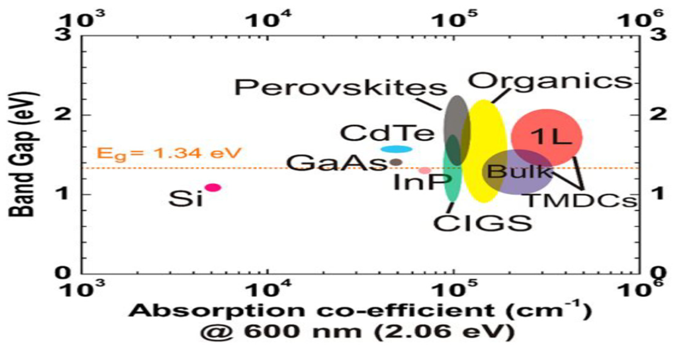
4. Photocells Based on 2D Crystals and Nanocomposites

Two-dimensional semiconductors provide unique opportunities for optoelectronics due to their layered atomic structure and optical and electronic properties. To date, most of the applied research in this area is focused on field-effect electronics, as well as photodetectors and LEDs. The photonic and electronic design of a 2D semiconductor photovoltaic system represents a new direction for ultra-thin, efficient solar cells with applications ranging from portable and ultra-lightweight optoelectronic battery power generation to intelligent photosensors. The absorption of light in the active layers of a photovoltaic cell is one of the key performance indicators that determines the efficiency of a device. For semiconductors, including 2D materials, absorption is determined by the structure of the electron band and the band gap. There is an inevitable trade-off between bandgap (voltage) and absorption (photocurrent). Figure 7 shows the values of the energy of the band gap and the absorption coefficients for the main photovoltaic materials studied to date on a commercial and research scale [25]. As can be seen from Figure 7 that of all the materials considered for photovoltaic applications with a band gap close to the optimal value for visible light of 1.34 eV, 2D transition metal dichalcogenides show the maximum absorption.
Figure 8a shows the characteristics and response times of various photodetector technologies (2D and modern technologies) and shows the direction to follow for competitive new technologies [25]. In the case of p-n junction photosensors in graphene, the speed of the photodetector is of paramount importance, especially when remote sensing in time or when transmitting data. A fast photodetector must also be sensitive enough to operate under real conditions (temperature, form factor, etc.). Two-dimensional materials can rapidly enter the infrared detector market through broadband absorption of graphene and combination with associated low-dimensional infrared sensitizers. Figure 8b illustrates the perspectives of using 2D photodetectors in terms of their superiority in performance and cost of currently used semiconductor infrared technologies, based mainly on InGaAs and HgCdTe photodiodes. If we compare the sensitivity and response time of standard and 2D photosensors, as well as their specific detectivity for different wavelengths, then 2D photosensors based on MoS2 and graphene are superior to standard technologies for the 1–5 μm range. Thus, the use of low-dimensional materials can solve the problem of creating inexpensive, highly sensitive IR sensors for machine vision.
MoS2/GO heterostructures and nanocomposite materials make it possible to create structures with controlled absorption in a wide range from UV to IR, due to the formation of self-organizing MoS2 (Eg = 1.3–1.9 eV)/GO (Eg = 0–6 eV) heterostructures [27]. MoS2/rGO nanocomposites synthesized using preliminary ultrasonic treatment and a one-stage hydrothermal and reduction process are self-organizing MoS2 nanocrystals in a reduced GO (rGO) matrix [27]. The effect of quantum confinement in nanostructures controlled by the degree of reduction of graphene oxide and the size of graphene and MoS2 nanocrystals led to tunable optical absorption in a wide UV–IR wavelength range from 280 to 973 nm (Figure 9). Low-dimensional layered MoS2/rGO heterostructures have great potential for creating high-performance broadband photosensors.

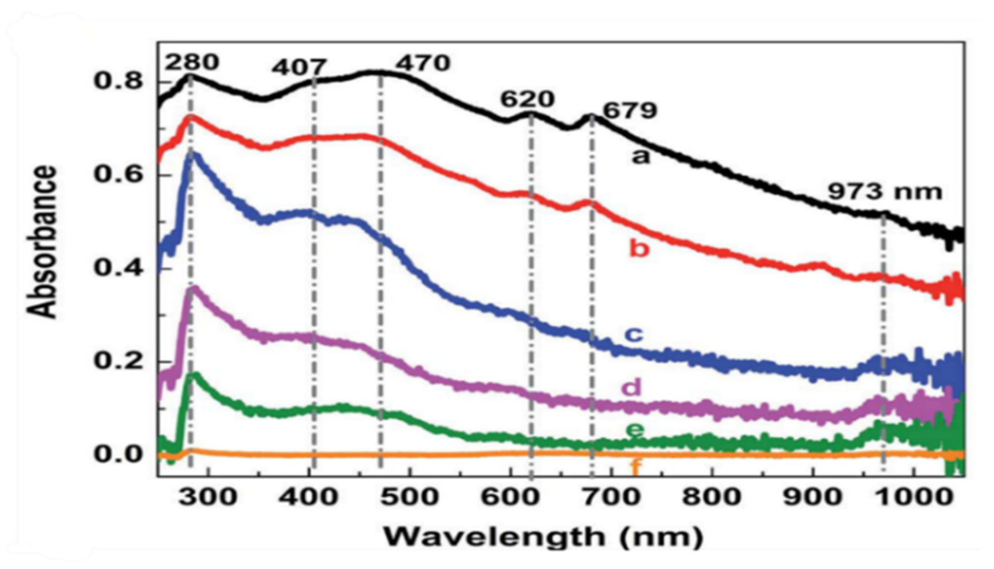
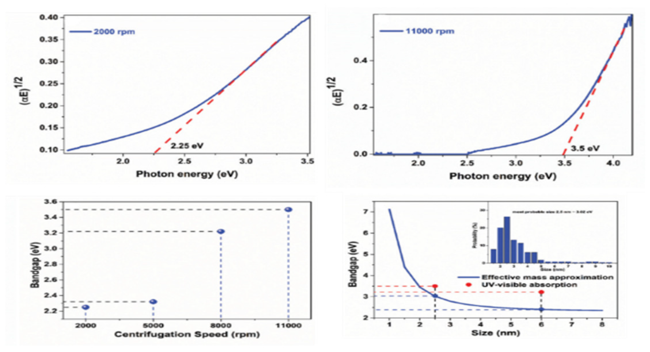
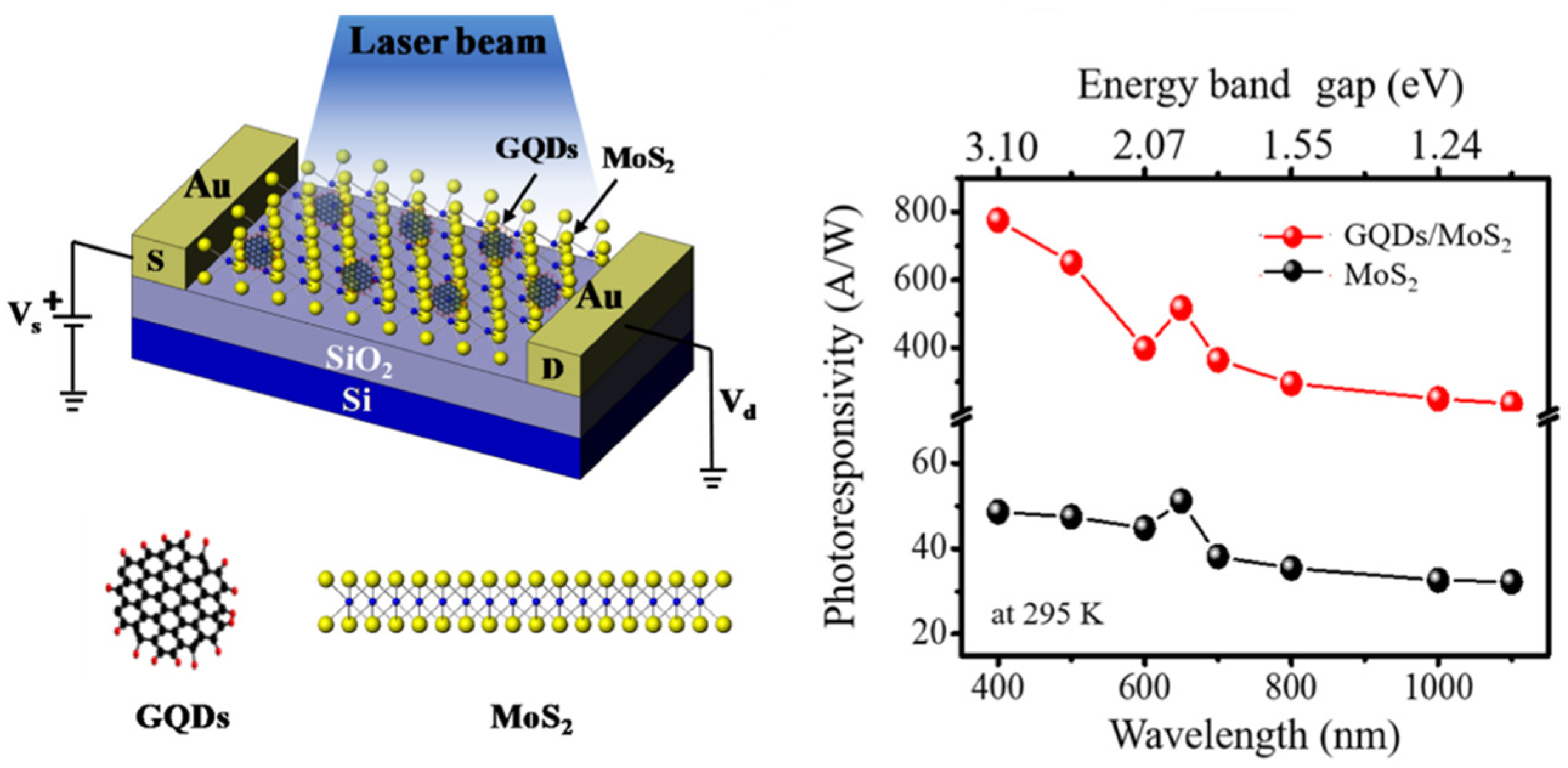
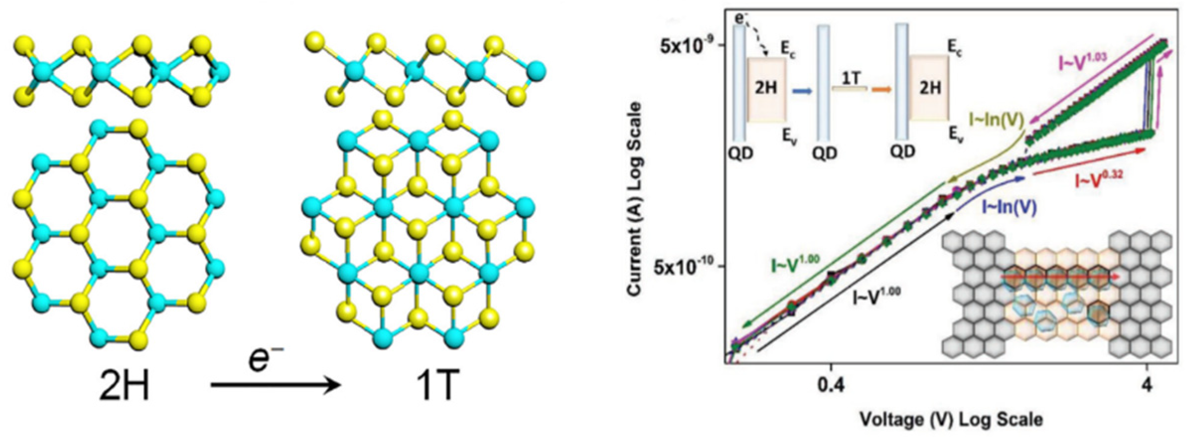
5. Layered Quantum Dots

Layered materials have recently emerged as layered atomically thin QDs consisting of only a few layers or even a single layer of material with transverse dimensions of less than 10 nm [28,29,30,31,32,33,34,35]. The band gap of such QDs can be tuned by optimizing their lateral size and the number of layers. Layered QDs have unique luminescent, adsorption, and chemical properties due to their inherent two-dimensional structure. Most layered QDs retain their two-dimensional lattices from their bulk form, but with improved solution dispersibility and surface functionalization capabilities. With a greater surface area, higher solubility, and heterostructure formation flexibility, QD-based devices can be modified to provide better performance and stability characteristics [34,35].
The formation of quantum dots consisting of one or several 4H-SnS2 layers was demonstrated by the liquid-phase separation method [28]. With a decrease in their size, a systematic shift of the peaks in the Raman and absorption spectra was observed. The band gap of QDs, estimated from absorption spectra and tunneling spectroscopy using graphene electrodes, varied from 2.25 to 3.50 eV with decreasing QD size (Figure 10) [28]. Single-layer QDs 2–4 nm in size, transparent in the visible region, showed selective absorption and photosensitivity at wavelengths in the ultraviolet region of the spectrum, while larger multilayer quantum dots (5–90 nm) showed broadband absorption in the visible region of the spectrum and good photoresponse when excited by white light. Layered QDs exhibited a well-controlled band gap and absorption over a wide tunable wavelength range. Such layered QDs, obtained using an economical method of separation and deposition on various substrates at room temperature, can be used to form high-performance broadband photomemristive heterostructures embedded in CMOS technology.
Layered quantum dots have also been obtained using plasma processing. Studies of photoluminescence and atomic force microscopy of bilayer graphene treated with nitrogen plasma revealed the formation of localized nanoscale features, the properties of which are determined by the processing modes (Figure 11) [29]. Using Raman scattering and spectroscopic ellipsometry, the effects of doping caused by oxygen or nitrogen plasma on the optical properties of single-layer and double-layer CVD graphene were investigated. Excitation at a wavelength of 250 nm of bilayer graphene treated with nitrogen plasma leads to photoluminescence in a wide spectral range with peaks at 390, 470, and 620 nm (Figure 11), which is consistent with the formation of quantum dots sensitive in the UV–IR range.
A hybrid structure consisting of zero-dimensional (0D) GQD and 2D MoS2 has demonstrated remarkable properties for optoelectronic devices, outperforming MoS2 photodetectors [31]. GQDs have unique optoelectronic characteristics such as long carrier lifetimes and fast electron-extraction due to huge transition energies and weak coupling to exciton states. When GQDs interact with 2D materials, quantum effects can influence the dynamics of charge carriers, enabling the efficient separation, transport, and collection of charge carriers. Hybrid GQD/MoS2 photodetectors are shown in Figure 12.
The photoelectric mechanism of this device consists of various physical stages of photoexcitation, reabsorption, tunneling, and thermal excitation. When the energy of incoming photons exceeds the GQD band gap, photoexcitation occurs in MoS2 and GQD. Then, the process of re-absorption of photons emitted by GQD, MoS2 is detected, thereby increasing the photocurrent by creating more electron–hole pairs. Thereafter, photoexcited electrons in the GQD conduction band are injected into MoS2 to initiate the tunneling process. Similarly, holes from the MoS2 valence band will be transferred to the GQD, resulting in a higher recombination rate. In addition, the formation of a Schottky barrier at the GQD–MoS2 interface leads to thermal excitation of higher-energy electrons from the GQD to MoS2. As a result of several charge carrier amplification processes, the photoresponse of hybrid GQD/MoS2 devices will be higher than that of bare MoS2 devices. Using a tunable laser source for optical illumination, the photoresponse of hybrid GQD/MoS2 devices and bare MoS2 devices was analyzed as a function of wavelength, as shown in Figure 12. The photosensitivity of hybrid GQD/MoS2 was found to be 775 AW−1 at a laser wavelength of 400 nm, while the photosensitivity of bare MoS2 is 44.8 AW−1. Compared to previous studies of photodetectors based on other material systems such as CuPc and CdTe, the experimentally determined photosensitivity is more than 300 times higher [31,32]. In addition, the hybrid GQD/MoS2 device exhibits a detectivity of 2.33 × 10¹² Jones and an EQE (~241%) that is almost 17 times higher than that of a simple MoS2 device (~14%).
To create fast and energy-efficient photomemristive devices, quantum dot structures with 2D MoS2 layers have been investigated [36]. Memristor structures based on low-dimensional materials demonstrate low energy consumption and the ability to achieve ultra-high cell density. The photoinduced phase transition in the structure of 2D MoS2 with 0D QDs provides dynamic photoresistive memory (Figure 13) [36,37]. The excitation of MoS2 nanocrystals by a laser with a wavelength of 530 nm leads to an ultrafast (~fs) 2H-1T phase transition from a semiconductor to a metal with a change in electrical resistance. The photoinduced 2H-1T phase transition in MoS2 occurs when the laser radiation density changes from 0.2 to 1.02 mW/μm−2 and is reversible. Changes in the current and temperature in such a structure led to dynamic photomemristive switching and a shift in the switching threshold upon optical excitation. Resistive switching of the structure is observed in an electric field and can be controlled by local photoexcitation of QDs. The photoinduced phase transition upon excitation of QDs leads to multilevel stochastic states similar to those in a biological synapse. The dynamic photomemristive structure demonstrates great potential for detection and computation required for rapid real-time pattern recognition and photoconfiguration of neural networks over a wide spectral range.

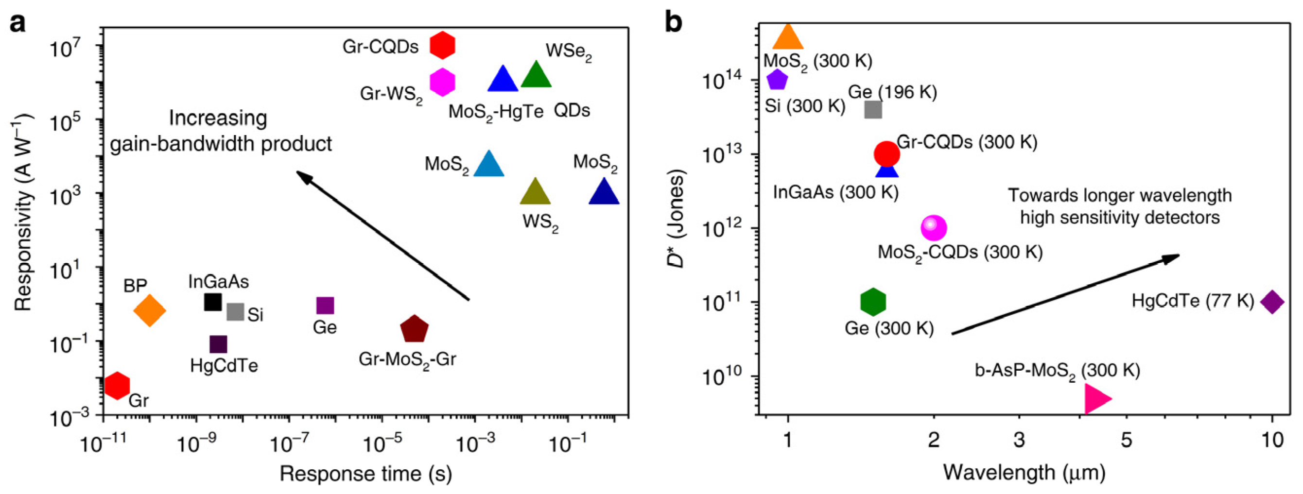
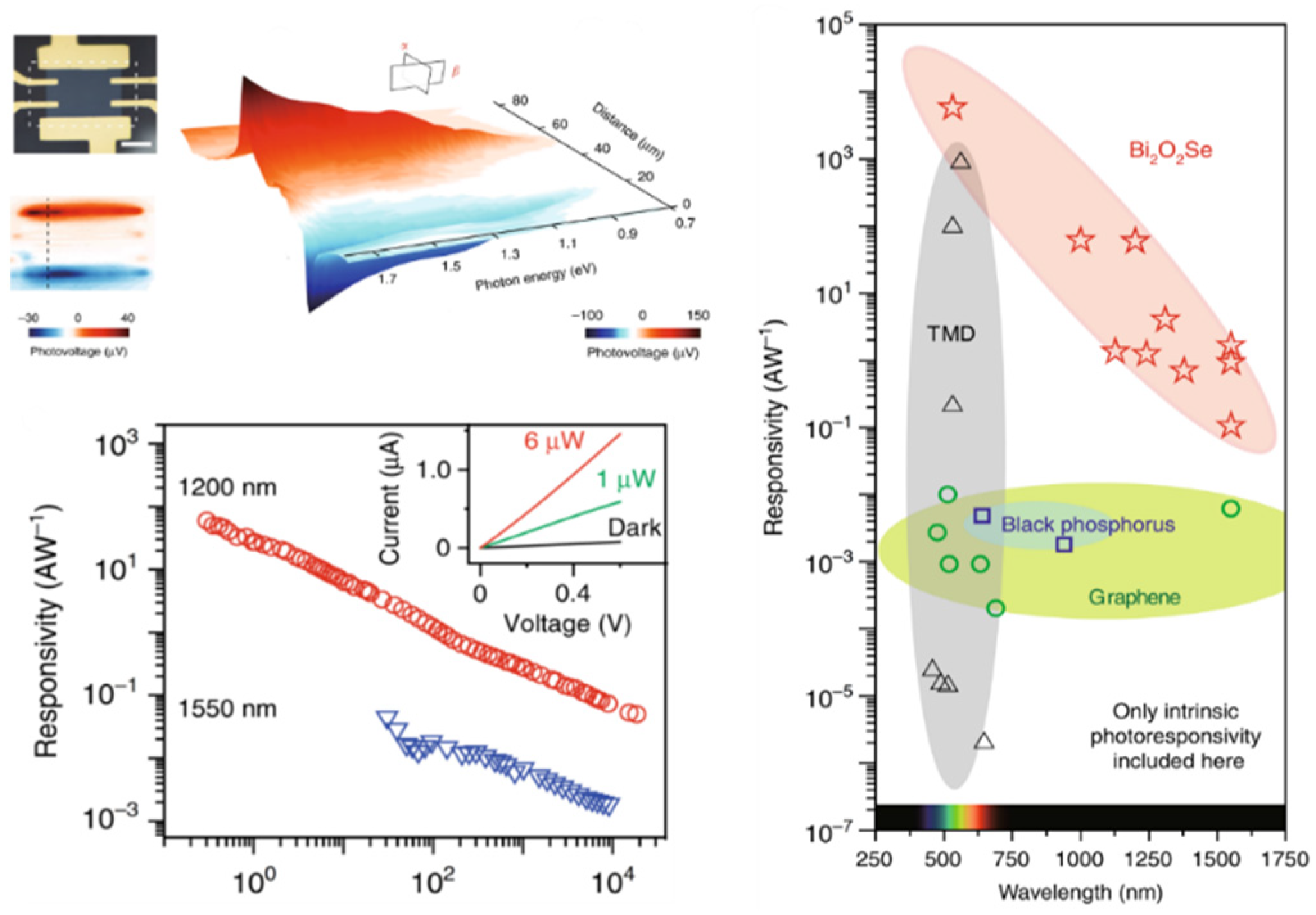
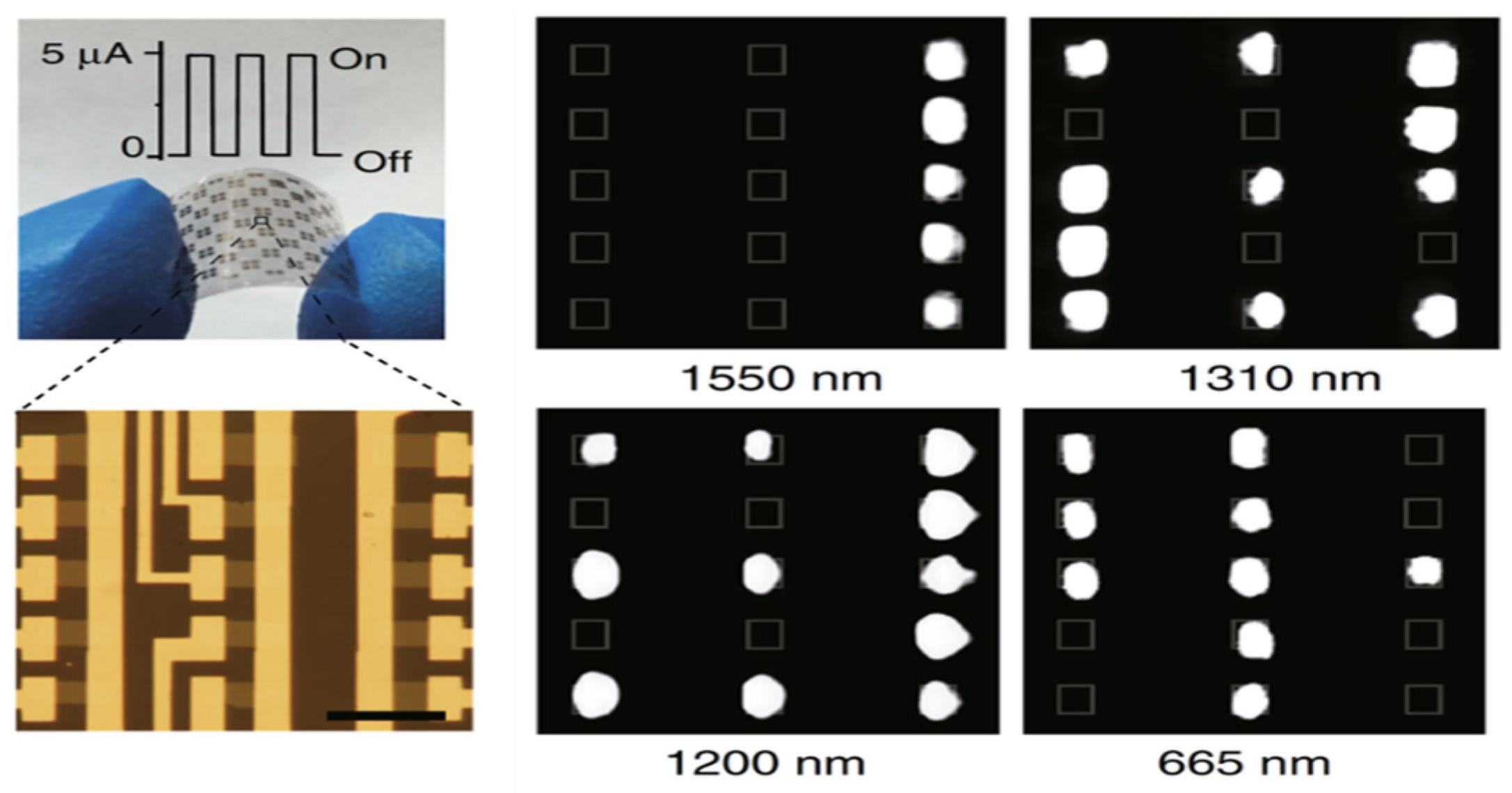
6. Ultrafast and Highly Sensitive IR Photosensors Based on 2D Crystals for Pattern Recognition

Detection and sensing by infrared light are widely used in modern technologies, which are based on various photovoltaic materials. The emergence of 2D materials, due to their excellent electronic structure, extreme size limitation, and strong interaction of light and matter, creates a unique platform for the development of next-generation infrared photosensors, see Table 1 [38,39,40,41].
Many 2D materials exhibit high environmental and chemical resistance, ideal mechanical, electronic, and optical properties required for industrial applications [48,49,50,51,52,53]. Ideal infrared detectors have fast response times, high sensitivity, and environmental resistance, which are rarely found simultaneously in the same two-dimensional material. An ultrafast and highly sensitive IR photodetector based on a 2D Bi2O2Se crystal was recently demonstrated [45]. The photodetector showed a high responsivity of 65 A/W at a wavelength of 1.2 μm and an ultrafast photoresponse of ~1 ps at room temperature, which corresponds to a bandwidth limited by the material up to 500 GHz. Figure 14 shows the characteristics of a Bi2O2Se photosensor under a bias of 0.6 V for wavelengths of 1.2 and 1.5 μm. It can be seen that the photosensor demonstrates responsivity in a wide region of the visible–IR range from 500 to 1500 nm.
Figure 15 shows the data on an oxyselenide 2D photosensor array used for pattern recognition.
The 2D Bi2O2Se photodetector quantifies the infrared reflection of the sample structure by measuring the detected photocurrent. When scanning the structure, the recorded values of the reflection signals are converted into an image. For different wavelengths—1.5, 1.3, 1.2 µm, and 665 nm—photocurrent images were obtained with shapes 1, 2, 3, and 4, respectively. The imaging capability, combined with high responsivity, ultra-fast photoresponse, and chemical stability, makes 2D Bi2O2Se a promising candidate for the implementation of ultra-fast and sensitive infrared photosensors for image recognition operating at room temperature.

7. Conclusions and Perspectives

Low-dimensional layered (LDL) photosensitive memristive materials and structures offer good scalability, and the potential for photodetection and in-memory computing is seen as a promising candidate for next-generation broadband CMOS-compatible image-recognition devices for AI applications in autonomous unmanned vehicles. Photomemristor and photosensor structures based on two-dimensional crystals and van der Waals heterostructures are a new class of optoelectronic components for autonomous energy-saving neuromorphic visual information processing systems. The use of a floating QD photogate makes it possible to optically control multilevel photomemristive states in a wide visible–IR range. However, researchers are still looking for ideal LDL photomemristive devices, as modern photomemristors based on charge trapping and phase transitions produce non-linear and asymmetric responses. In addition, it is still quite difficult to develop proper processes for the fabrication of optoelectronic devices based on LDL materials using conventional semiconductor technology. Another important issue of LDL materials for photosynaptic applications is reliability. The quality of LDL material crystals, a key factor in desired photosynaptic operations, depends on various synthesis conditions or growth methods. In addition, at present, many studies are mainly focused on the optical and electrical properties of LDL materials, while more attention to their mechanical and magnetic properties can significantly improve the performance of photomemristive sensors. Photodetectors based on LDL materials are of great interest due to their wide photodetection range, high sensitivity, flexibility, and potentially small size. With these advantages, it is possible to revolutionize the mid-IR photodetector industry in favor of compact, small-sized and low-cost visible–IR smart photodetectors that can be used in an AI visual system. The nature of the atomic layer and the broadband photoresponse of LDL materials will be an important part of the next-generation broadband artificial vision industry. However, it remains a big challenge to obtain LDL photosensors with high response speed, high gain, and high detectability at the same time, especially in the mid- and far-IR range. Bismuth oxyselenide has excellent physical properties due to its unique crystal configuration and electronic structure, such as ultra-high mobility, good mechanical flexibility, and broadband optical response. Due to its oxygen-containing composition, its remarkable stability makes it a competitive candidate for practical applications in optoelectronics. However, a simple, large-scale, and inexpensive synthesis of the LDL bismuth oxyselenide structure remains a challenging task. Most existing LDL photomemristive devices currently cannot meet the requirements of a commercially ideal photoelectronic synapses. However, there are huge opportunities for improving the technology of manufacturing and storing data, processing optical signals for truly autonomous unmanned vehicles. This will likely require a coordinated effort from researchers across disciplines, including materials, devices, circuits, and architecture.

Funding

This research was funded by the Russian Foundation for Basic Research (RFBR), Grant No. 19-29-03050 and State Assignment of the Ministry of Science and Higher Education of the Russian Federation № 075-00706-22-00. The APC was funded by RFBR.

Conflicts of Interest

The author declare no conflict of interest.

References

  1. Panin, G.N.; Kapitanova, O.O. Memristive Systems Based on Two-Dimensional Materials. In Advances in Memristor Neural Networks—Modeling and Applications; Ciufudean, C., Ed.; IntechOpen: London, UK, 2018; pp. 67–88. [Google Scholar] [CrossRef] [Green Version]
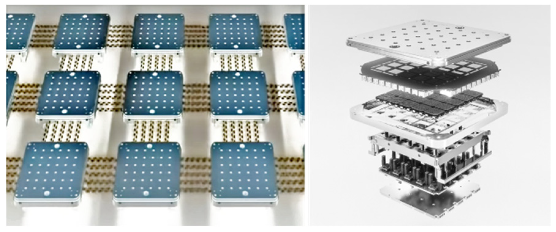
  2. Tesla’s BREAKTHROUGH DOJO Supercomputer Hardware Explained. Available online: https://www.youtube.com/watch?v=pPHX7e1BxSM (accessed on 1 September 2021).
  3. Unified Energy System of Russia: Interim Results. November 2021. Available online: https://www.so-ups.ru/fileadmin/files/company/reports/ups-review/2021/ups_review_1121.pdf (accessed on 1 December 2021). (In Russian).
  4. Ielmini, D.; Wong, H.-S.P. In-memory computing with resistive switching devices. Nat. Electron. 2018, 1, 333–343. [Google Scholar] [CrossRef]
  5. Im, I.H.; Kim, S.J.; Jang, H.W. Memristive Devices for New Computing Paradigms. Adv. Intell. Syst. 2020, 2, 2000105. [Google Scholar] [CrossRef]
  6. Wan, Q.; Sharbati, M.T.; Erickson, J.R.; Du, Y.; Xiong, F. Emerging Artificial Synaptic Devices for Neuromorphic Computing. Adv. Mater. Technol. 2019, 4, 1900037. [Google Scholar] [CrossRef] [Green Version]
  7. Mehonic, A.; Sebastian, A.; Rajendran, B.; Simeone, O.; Vasilaki, E.; Kenyon, A.J. Memristors—From In-Memory Computing, Deep Learning Acceleration, and Spiking Neural Networks to the Future of Neuromorphic and Bio-Inspired Computing. Adv. Intell. Syst. 2020, 2, 2000085. [Google Scholar] [CrossRef]
  8. Bian, H.; Goh, Y.Y.; Liu, Y.; Ling, H.; Xie, L.; Liu, X. Stimuli-Responsive Memristive Materials for Artificial Synapses and Neuromorphic Computing. Adv. Mater. 2021, 33, 2006469. [Google Scholar] [CrossRef]
  9. Choi, S.; Yang, J.; Wang, G. Emerging Memristive Artificial Synapses and Neurons for Energy-Efficient Neuromorphic Computing. Adv. Mater. 2020, 32, 2004659. [Google Scholar] [CrossRef]
  10. Wang, C.-Y.; Wang, C.; Meng, F.; Wang, P.; Wang, S.; Liang, S.-J.; Miao, F. 2D Layered Materials for Memristive and Neuromorphic Applications. Adv. Electron. Mater. 2020, 6, 1901107. [Google Scholar] [CrossRef] [Green Version]
  11. Cao, G.M.; Meng, P.; Chen, J.; Liu, H.; Bian, R.; Zhu, C.; Liu, F.; Liu, Z. 2D Material Based Synaptic Devices for Neuromorphic Computing. Adv. Funct. Mater. 2021, 31, 2005443. [Google Scholar] [CrossRef]
  12. Sun, L.; Wang, W.; Yang, H. Recent Progress in Synaptic Devices Based on 2D Materials. Adv. Intell. Syst. 2020, 2, 1900167. [Google Scholar] [CrossRef] [Green Version]
  13. Panin, G.N. Optoelectronic dynamic memristor systems based on two-dimensional crystals. Chaos Solitons Fractals 2021, 142, 110523. [Google Scholar] [CrossRef]
  14. Panin, G.N. Memristive two-dimensional electronic systems—A new type of logic switches and memory. Electronic Engineering. Series 3. Microelectronics 2018, 1, 23–41. (In Russian) [Google Scholar]
  15. Wang, W.; Panin, G.N.; Fu, X.; Zhang, L.; Ilanchezhiyan, P.; Pelenovich, V.; Fu, D.; Kang, T.W. MoS2 memristor with photoresistive switching. Sci. Rep. 2016, 6, 31224. [Google Scholar] [CrossRef] [PubMed] [Green Version]
  16. Kapitanova, O.O.; Emelin, E.V.; Dorofeev, S.G.; Evdokimov, P.V.; Panin, G.N.; Lee, Y.; Lee, S. Direct patterning of reduced graphene oxide/graphene oxide memristive heterostructures by electron-beam irradiation. J. Mater. Sci. Technol. 2020, 38, 237–243. [Google Scholar] [CrossRef]
  17. Alzakia, F.I.; Tan, S.C. Liquid-Exfoliated 2D Materials for Optoelectronic Applications. Adv. Sci. 2021, 8, 2003864. [Google Scholar] [CrossRef] [PubMed]
  18. Jiang, J.; Wen, Y.; Wang, H.; Yin, L.; Cheng, R.; Liu, C.; Feng, L.; He, J. Recent Advances in 2D Materials for Photodetectors. Adv. Electron. Mater. 2021, 7, 2001125. [Google Scholar] [CrossRef]
  19. Kaushik, S.; Singh, R. 2D Layered Materials for Ultraviolet Photodetection: A Review. Adv. Optical Mater. 2021, 9, 2002214. [Google Scholar] [CrossRef]
  20. Kapitanova, O.O.; Panin, G.N.; Cho, D.H.; Baranov, N.A.; Kang, W.T. Formation of Self-Assembled Nanoscale GrapheneGraphene Oxide Photomemristive Heterojunctions using Photocatalytic Oxidation. Nanotechnology 2017, 28, 204005. [Google Scholar] [CrossRef]
  21. Rogalski, A.; Martyniuk, P.; Kopytko, M.; Hu, W. Trends in Performance Limits of the HOT Infrared Photodetectors. Appl. Sci. 2021, 11, 501. [Google Scholar] [CrossRef]
  22. Goossens, S.; Navickaite, G.; Monasterio, C.; Gupta, S.; Piqueras, J.J.; Pérez, R.; Burwell, G.; Nikitskiy, I.; Lasanta, T.; Galán, T.; et al. Broadband image sensor array based on graphene–CMOS integration. Nat. Photonics 2017, 11, 366–371. [Google Scholar] [CrossRef]
  23. Rauch, T.; Böberl, M.; Tedde, S.F.; Fürst, J.; Kovalenko, M.; Hesser, G.; Lemmer, U.; Heiss, W.; Hayden, O. Near-infrared imaging with quantum-dot-sensitized organic photodiodes. Nat. Photonics 2009, 3, 332–336. [Google Scholar] [CrossRef]
  24. Nikitskiy, I.; Goossens, S.; Kufer, D.; Lasanta, T.; Navickaite, G.; Koppens, F.H.L.; Konstantatos, G. Integrating an electrically active colloidal quantum dot photodiode with a graphene phototransistor. Nat. Commun. 2016, 7, 11954. [Google Scholar] [CrossRef] [PubMed] [Green Version]
  25. Jariwala, D.; Davoyan, A.R.; Wong, J.; Atwater, H.A. Van der Waals Materials for Atomically-Thin Photovoltaics: Promise and Outlook. ACS Photonics 2017, 4, 2962–2970. [Google Scholar] [CrossRef] [Green Version]
  26. Konstantatos, G. Current status and technological prospect of photodetectors based on two-dimensional materials. Nat. Commun. 2018, 9, 5266. [Google Scholar] [CrossRef] [PubMed]
  27. Wang, W.; Kapitanova, O.O.; Ilanchezhiyan, P.; Xi, S.; Panin, G.N.; Fu, D.; Kang, T.W. Self-assembled MoS2/rGO nanocomposites with tunable UV-IR absorption. RSC Adv. 2018, 8, 2410–2417. [Google Scholar] [CrossRef]
  28. Fu, X.; Ilanchezhiyan, P.; Kumar, G.M.; Cho, H.D.; Zhang, L.; Chan, A.S.; Lee, D.J.; Panin, G.N.; Kang, T.W. Tunable UV-visible absorption of SnS2 layered quantum dots produced by liquid phase exfoliation. Nanoscale 2017, 9, 1820–1826. [Google Scholar] [CrossRef]
  29. Kovaleva, N.N.; Chvostova, D.; Potucek, Z.; Cho, H.D.; Fu, X.; Fekete, L.; Pokorny, J.; Bryknar, Z.; Kugel, K.I.; Dejneka, A.; et al. Efficient green emission from edge states in graphene perforated by nitrogen plasma treatment. 2D Mater. 2019, 6, 045021. [Google Scholar] [CrossRef] [Green Version]
  30. Singh, K.J.; Ahmed, T.; Gautam, P.; Sadhu, A.S.; Lien, D.H.; Chen, S.C.; Chueh, Y.; Kuo, H.C. Recent Advances in Two-Dimensional Quantum Dots and Their Applications. Nanomaterials 2021, 11, 1549. [Google Scholar] [CrossRef]
  31. Min, M.; Sakri, S.; Saenz, G.A.; Kaul, A.B. Photophysical Dynamics in Semiconducting Graphene Quantum Dots Integrated with 2D MoS2 for Optical Enhancement in the Near UV. ACS Appl. Mater. Interfaces 2021, 13, 5379–5389. [Google Scholar] [CrossRef]
  32. Chen, C.; Qiao, H.; Lin, S.; Luk, C.M.; Liu, Y.; Xu, Z.; Song, J.; Xue, Y.; Li, D.; Yuan, J.; et al. Highly responsive MoS2 photodetectors enhanced by graphene quantum dots. Sci. Rep. 2015, 5, 11830. [Google Scholar] [CrossRef]
  33. Zhang, K.; Fu, L.; Zhang, W.; Pan, H.; Sun, Y.; Ge, C.; Du, Y.; Tang, N. Ultrasmall and Monolayered Tungsten Dichalcogenide Quantum Dots with Giant Spin–Valley Coupling and Purple Luminescence. ACS Omega 2018, 3, 12188–12194. [Google Scholar] [CrossRef]
  34. Kortel, M.; Mansuriya, B.D.; Vargas Santana, N.; Altintas, Z. Graphene Quantum Dots as Flourishing Nanomaterials for Bio-Imaging, Therapy Development, and Micro-Supercapacitors. Micromachines 2020, 11, 866. [Google Scholar] [CrossRef] [PubMed]
  35. Tajik, S.; Dourandish, Z.; Zhang, K.; Beitollahi, H.; van Le, Q.; Jang, H.W.; Shokouhimehr, M. Carbon and graphene quantum dots: A review on syntheses, characterization, biological and sensing applications for neurotransmitter determination. RSC Adv. 2020, 10, 15406–15429. [Google Scholar] [CrossRef] [Green Version]
  36. Fu, X.; Zhang, L.; Cho, H.D.; Kang, T.W.; Fu, D.; Lee, D.; Lee, S.W.; Li, L.; Qi, T.; Chan, A.S.; et al. Molybdenum disulfide nanosheet/quantum dot dynamic memristive structure driven by photoinduced phase transition. Small 2019, 15, e1903809. [Google Scholar] [CrossRef]
  37. Panin, G.N. Optoelectronic memristors based on two-dimensional crystals for neural networks. Nanoindustry 2020, 13, 704–717. (In Russian) [Google Scholar] [CrossRef]
  38. An, J.; Wang, B.; Shu, C.; Wu, W.; Sun, B.; Zhang, Z.; Li, D.; Li, S. Research development of 2D materials based photodetectors towards mid-infrared regime. Nano Sel. 2021, 2, 527–540. [Google Scholar] [CrossRef]
  39. Wang, F.K.; Zhang, Y.; Gao, Y.; Luo, P.; Su, J.W.; Han, W.; Liu, K.L.; Li, H.Q.; Zhai, T.Y. 2D Metal Chalcogenides for IR Photodetection. Small 2019, 15, 1901347. [Google Scholar] [CrossRef]
  40. Wang, F.; Yang, S.; Wu, J.; Hu, X.; Li, Y.; Li, H.; Liu, X.; Luo, J.; Zhai, T. Emerging two-dimensional bismuth oxychalcogenides for electronics and optoelectronics. InfoMat 2021, 3, 1251–1271. [Google Scholar] [CrossRef]
  41. Li, J.; Wang, Z.; Wen, Y.; Chu, J.; Yin, L.; Cheng, R.; Lei, L.; He, P.; Jiang, C.; Feng, L.; et al. High-Performance Near-Infrared Photodetector Based on Ultrathin Bi2O2Se Nanosheets. Adv. Funct. Mater. 2018, 28, 1706437. [Google Scholar] [CrossRef]
  42. Yin, Z.; Li, H.; Li, H.; Jiang, L.; Shi, Y.; Sun, Y.; Lu, G.; Zhang, Q.; Chen, X.; Zhang, H. Single-Layer MoS2 Phototransistors. ACS Nano 2012, 6, 74–80. [Google Scholar] [CrossRef] [Green Version]
  43. Gul, H.Z.; Sakong, W.; Ji, H.; Torres, J.; Yi, H.; Ghimire, M.K.; Yoon, J.H.; Yun, M.H.; Hwang, H.R.; Lee, Y.H.; et al. Semimetallic Graphene for Infrared Sensing. ACS Appl. Mater. Interfaces 2019, 11, 19565. [Google Scholar] [CrossRef]
  44. Fang, Z. Plasmonic silicon quantum dots extend photodetection into mid-infrared range. Sci. Bull. 2017, 62, 1430–1431. [Google Scholar] [CrossRef] [Green Version]
  45. Yin, J.; Tan, Z.; Hong, H.; Wu, J.; Yuan, H.; Liu, Y.; Chen, C.; Tan, C.; Yao, F.; Li, T.; et al. Ultrafast and highly sensitive infrared photodetectors based on two-dimensional oxyselenide crystals. Nat. Commun. 2018, 9, 3311. [Google Scholar] [CrossRef] [PubMed]
  46. Massicotte, M.; Schmidt, P.; Vialla, F.; Schädler, K.G.; Reserbat-Plantey, A.; Watanabe, K.; Taniguchi, T.; Tielrooij, K.J.; Koppens, F.H. Picosecond Photoresponse in van der Waals Heterostructures. Nat. Nanotechnol. 2015, 11, 42. [Google Scholar] [CrossRef] [PubMed]
  47. Pak, J.; Jang, J.; Cho, K.; Kim, T.-Y.; Kim, J.-K.; Song, Y.; Hong, W.-K.; Min, M.; Lee, H.; Lee, T. Enhancement of Photodetection Characteristics of MoS2 Field Effect Transistors Using Surface Treatment with Copper Phthalocyanine. Nanoscale 2015, 7, 18780–18788. [Google Scholar] [CrossRef]
  48. Geim, A.K.; Grigorieva, I.V. Van der Waals heterostructures. Nature 2013, 499, 419–425. [Google Scholar] [CrossRef]
  49. Wang, X.; Li, G.; Feng, X.; Nielsch, K.; Golberg, D.; Schmidt, O.G. Chemical and structural stability of 2D layered materials. 2D Mater. 2019, 6, 042001. [Google Scholar] [CrossRef]
  50. Qiao, H.; Liu, H.; Huang, Z.; Hu, R.; Ma, Q.; Zhong, J.; Qi, X. Tunable Electronic and Optical Properties of 2D Monoelemental Materials Beyond Graphene for Promising Applications. Energy Environ. Mater. 2021, 4, 522–543. [Google Scholar] [CrossRef]
  51. Weng, Q.; Li, G.; Feng, X.; Nielsch, K.; Golberg, D.; Schmidt, O.G. Electronic and Optical Properties of 2D Materials Con-structed from Light Atoms. Adv. Mater. 2018, 30, 1801600. [Google Scholar] [CrossRef] [Green Version]
  52. Gong, C.; Zhang, Y.; Chen, W.; Chu, J.; Lei, T.; Pu, J.; Dai, L.; Wu, C.; Cheng, Y.; Zhai, T.; et al. Electronic and Optoelectronic Applications Based on 2D Novel Anisotropic Transition Metal Dichalcogenides. J. Adv. Sci. 2017, 4, 1700231. [Google Scholar] [CrossRef]
  53. Roy, S.; Zhang, X.; Puthirath, A.B.; Meiyazhagan, A.; Bhattacharyya, S.; Rahman, M.M.; Babu, G.; Susarla, S.; Saju, S.K.; Tran, M.K.; et al. Structure, Properties and Applications of Two-Dimensional Hexagonal Boron Nitride. Adv. Mater. 2021, 33, 2101589. [Google Scholar] [CrossRef]
Figure 1. A set of D1 Dojo processors (2021) for Tesla’s AI autopilot, designed to work in neural networks (left). The design of the processor, consisting of various plates: heat sink, computation, and power and control (right).
Electronics 11 00619 g001
Figure 2. Computational architecture of Von Neumann.
Electronics 11 00619 g002
Figure 3. Current–voltage characteristics of the MoS2 photomemristor polarized at 3V (left, top) and 6V (left, bottom) and switching diagrams (SET, RESET) of memristive states (HRSD3, HRSL3, LRSD3, LRSL3, HRSD6, HRSL6, LRSD6, LRSL6) with electrical and optical excitation [15].
Electronics 11 00619 g003
Figure 4. Schematic diagram of a graphene/GO-based photomemristor matrix on a Si/SiO2 substrate, formed by photocatalytic oxidation in the regions near ZnO nanoparticles (ZnO NPs) and a switching diagram (SET, RESET) of high-resistive (HRS) and low-resistive (LRS) states in the dark (HRSD, LRSD) and with photoexcitation (HRSL, LRSL) [20].
Electronics 11 00619 g004
Figure 5. Spectral sensitivity of photodetectors made of 2D layered materials at 300 K. The black line shows the spectral sensitivity of an ideal photodiode with 100% QE and g = 1. The sensitivity of commercially available photodetectors (InGaAs and HgCdTe photodiodes) is presented for comparison [21].
Electronics 11 00619 g005
Figure 6. CMOS integration of CVD graphene with image-sensor readout circuit. Embedding of transferred CVD graphene on a 15.1 mm-high and 14.3 mm-wide crystal containing a CMOS image-sensor readout circuit that consists of 388 × 288 pixels (left). Side view (right) showing a graphene photoconductor lying on a readout circuit. Graphene channels are sensitized to ultraviolet, visible, near-infrared, and short-wave infrared light using QDs: when light is absorbed, an electron–hole pair is generated; due to the built-in electric field, the hole turns into graphene, while the electron remains trapped in the QD [22].
Electronics 11 00619 g006
Figure 7. Energy of the band gap and coefficients of absorption for the main photosensitive materials investigated on a commercial and research scale [25].
Electronics 11 00619 g007
Figure 8. Responsivity (a) and detectivity (b) of 2D photodetector technologies and technologies currently in use [26].
Electronics 11 00619 g008
Figure 9. Broadband UV–IR absorption of layered MoS2/rGO nanocomposite in the wavelength range from 280 to 973 nm [27].
Electronics 11 00619 g009
Figure 10. Dependences of (αhν)1/2 on hν for SnS2 QDs, obtained from the absorption spectra in the UV–visible range at 2000 (left, top) and 11,000 rpm (right, top). Band gap of quantum dots obtained from UV–visible spectra of SnS2 nanocrystals formed at different centrifugation speeds (left, bottom). Dependence of the band gap of the SnS2 QD on the QD size, obtained in the effective mass approximation (blue line), and the band gap obtained from the spectra in the UV–visible range (red spheres) (right, bottom). The inset shows the distribution of QD sizes obtained at a speed of 11,000 rpm and the QD band gap calculated from the effective mass approximation [28].
Electronics 11 00619 g010
Figure 11. AFM image (left) of two graphene layers transferred onto a SiO2/Si substrate and processed in nitrogen plasma (scan size 600 × 600 nm2), and photoluminescence spectra (right) obtained by excitation of the resulting structure with light with λexc = 250 nm or 290 nm [29].
Electronics 11 00619 g011
Figure 12. Schematic of the GQD/MoS2 hybrid device under optical illumination (left). The insets show the corresponding molecular structures of GQD (top view) and MoS2 (side view). Photosensitivity of hybrid GQD/MoS2 (red) and bare MoS2 devices (black) versus wavelength at fixed Vds = 10 V with laser wavelength varying from 400 to 1100 nm at room temperature (right) [31].
Electronics 11 00619 g012
Figure 13. Crystal structure of MoS2 (left). Atoms in the lattice: molybdenum—yellow, sulfur—blue. Phase transition in MoS2 from a trigonal prismatic (D3h) to an octahedral (Oh) structure, induced by a negative charge. Current–voltage characteristic of the 2D MoS2 0D QD structure with graphene electrodes on a logarithmic scale (right). The inset at the top schematically shows a diagram of the photoexcited electron transfer process and the corresponding charging and discharging processes leading to 2H-1T phase transitions. The inset below shows a diagram of the formation of a filamentous channel from phase 1T. Graphene, 2H-MoS2, 1T-MoS2, and MoS2 QDs are displayed in gray, light yellow, brown, and blue, respectively.
Electronics 11 00619 g013
Figure 14. Optical image of a device based on Bi2O2Se ~ 10 nm-thick (~16 layers), scale bar 20 µm (top left). Scanning a photovoltaic device in the area marked with a dotted rectangle with a 1200 nm laser at 150 μW, recording the photovoltage as a function of the laser position without external bias (top middle). The spectrogram was obtained from the scanned photovoltage lines at various energies of the incident photons. Dependence of the photosensitivity of a 2D Bi2O2Se photodetector at a bias of 0.6 V at wavelengths of 1200 and 1500 nm on the incident power and bias voltage at a wavelength of 1200 nm (bottom left). Comparison of photodetectors based on Bi2O2Se, graphene, black phosphorus and transition metal dichalcogenides (TMD) (on right). The data include only the generation of a photocurrent due to the excitation of interband transitions without additional processing, such as the addition of waveguide or plasmonic structures [45].
Electronics 11 00619 g014
Figure 15. Flexible 2D arrays of Bi2O2Se photodetectors. Images of 2D Bi2O2Se photodetectors and arrays on mica (top left). The inset shows the photoresponse of one of the photodetectors when the substrate is bent with a deformation of up to 1%. The current rises at 1200 nm IR illumination with a power of about 100 μW. Photocurrent images with shapes 1, 2, 3, and 4 were obtained under illumination with light at 1550 nm, 1310 nm, 1200 nm, and 665 nm, respectively [45].
Electronics 11 00619 g015
Table 1. Characteristics of photodetectors based on low-dimensional layered materials and their heterostructures.
MaterialsResponsivity
(A W1)
Detectivity
(Jones)
Response
Time (ms)
Spectral
Range (μm)
Ref.
MoS29.0 × 1051 × 1071 × 103visible[42]
GQDs/MoS212.6 × 10216.1 × 10117.0 × 1010.400−1.100 [31]
Bi2O2Se6.58.3 × 10112.8UV–NIR[41]
Graphene-5 × 10⁸ 7–17[43]
G/SiQDs1 × 1091 × 1013-0.375–1.87[44]
Bi2O2Se653.0 × 1091 × 1091.2[45]
graphene/WSe24.4 × 1021 × 1085.5 × 109visible[46]
CuPc/MoS21.98 × 1006.1 × 10103 × 1020.405−0.780[47]
Publisher’s Note: MDPI stays neutral with regard to jurisdictional claims in published maps and institutional affiliations.

