1. Introduction
Compared with the traditional Von Neumann architecture computer, the human brain shows stronger associative memory and thinking in images. It also has a greater potential ability than existing computers in solving complex problems such as function approximation, complex classification and clustering [
1]. Moreover, compared with current existing computers, the human brain is not only more powerful, but it is also smaller and consumes less power. Therefore, the realization of the artificial neural network (ANN) to mimic the human brain intelligence has become a hot subject for research recently [
2]. The human brain is composed of many complex interconnected neurons, and the information interaction between neurons is what forms the thinking ability. Designing a reasonable and efficient neuron unit is an important point for imitating the thinking ability of the human brain [
3,
4].
The first-generation ANN consists of threshold gates [
5]. Its principle is using the threshold gate to judge the output result by counting the binary sum of the inputs. If the inputs’ summation is larger than the threshold value, it is considered to be high level (1); otherwise it is low level (0). It can be seen that the function of the first-generation ANN is very limited and that it can only process binary data. This is still far removed from the real biological neuron. The second-generation ANN is based on the encoding of the frequencies of the neuron pulses [
6]. By stacking multiple layers of the neurons and applying a back propagation algorithm, a neural network can be constructed, which is known as deep learning neural network. This network is widely used in machine learning, brain-machine interfaces, image sensors, etc. [
7]. Although the second-generation ANN is powerful, its energy consumption and efficiency are still not good enough compared with the biological network. Moreover, there is a big difference in the process of communicating with the spikes of neurons in the human brain in the underlying logic. Faced with these problems, the third-generation ANN has been proposed recently. Its neuron units are much closer to biological neurons, in that they can communicate with each other using spike signals. For this reason, it is also called spiking neural networks (SNN) [
8]. The neuron in the SNN is not activated in every iteration state. It can be activated only when the membrane voltage reaches a certain value. When a spike neuron is activated, it generates a spike signal, which is transmitted to other neurons [
9]. After the transmission, its membrane potential is changed accordingly. The spike generated by a biological neuron is used for encoding and processing the biological information. The artificial neural network shows a far superior ability in implementing real-time behavior systems or detailed large-scale simulations of neural systems than other digital tools and simulators [
10].
The retina is a key tissue and can obtain visuosensory information efficiently, a subject that has been intensively studied recently [
11,
12,
13]. By the pre-processing of optical information on the retina, the input light is transferred into the corresponding neural signal, which is encoded into the spike pattern for further transmission into a higher processor. Mimicking the biological retina, the artificial neuron model is designed based on CMOS technology, which is used to convert the optical pixel signals into specific spikes with certain frequencies. Billions of neurons with complex connections could build a large and efficient biological computing system.
Figure 1 shows the schematic diagrams of the biological retinal system and the artificial ones. With the very large number of retinal cells in the artificial neuron structure, it is important to optimize the energy efficiency of the artificial neurons by reducing the power consumption. One of the most important issues of the artificial neuron in a neuromorphic system is how to decrease the power consumption.
With the continuous investigation of the working mechanism of neurons, some artificial neuron circuits have been proposed. In [
14], a neuron circuit based on the leaky integrate-and-fire (LIF) model is proposed. This circuit can realize the spike timing dependent plasticity (STDP) function of the neuron [
15]. However, due to the existence of the multiple trans-conductance amplifiers in the circuit, the power is too high to be implemented practically. In [
16], a circuit based on the Morris-Lecar (ML) model is proposed, as shown in
Figure 2. Because the ML model is similar to the ion transport mechanism of the real neurons, the circuit can be used to mimic the real neurons [
17]. However, due to the existence of many conductive paths in the circuit, its static power consumption is relatively high. Moreover, the adopted large capacitances Cm and CK limit its operating frequency. In [
18], the circuit is simplified to reduce its power consumption, making the circuit display excellent merits in terms of its power consumption and area. However, the circuit is unstable and susceptible to the influences of the PVT variables.
In this paper, a novel artificial neuron circuit is proposed that has ultra-low power while keeping robust variation tolerance. The circuit shows minimum layout area and can be integrated into large-scale arrays for mimicking the biological systems. The structure of the proposed artificial neuron circuit is described in the paper. The analysis and the results of the artificial neuron retina are reported.
2. The Principle of Axon-Hillock Circuit
Figure 3 shows the Axon-Hillock circuit, which is considered to be the traditional artificial neuron circuit [
19]. It was proposed by Mead in 1989 and has been widely used in many works [
20,
21]. The input current I
in is commonly generated by a photodiode, in which different light intensities correspond to different magnitudes of the induced currents. The current I
in charges the membrane capacitor C
mem. The capacitor C
mem is the model of the retinal neuron’s membrane with the ionic current across it.
The amplifier in
Figure 3 is the main part for the generation of the neuron spike, in which two invertors, inv1 and inv2, are included. At the initial state, both the values of V
out and V
mem are zero. The capacitor C
mem is charged by I
in, so that the voltage V
mem on C
mem is pulled up by the charging current. When V
mem exceeds the threshold voltage of inv1, the invertor flips and a spike signal is generated by the output port. At this moment, V
out is at a high enough level to turn on the reset transistor, Mreset. The reset current is set by V
pw. If it is larger than the input current I
in, the membrane capacitor is discharged. Therefore, V
mem is decreased continuously until it reaches the amplifier’s switching threshold again. In this way, a cycle is finished and the next cycle starts again.
The circuit in
Figure 3 can imitate the characteristics of a stimulated retinal neuron, in which the output of the electric spike signal with a certain frequency can be generated and adjusted. It is a kind of classical SNN circuit. Based on the circuit, some research works propose useful solutions on how to reduce the power consumption. In [
18], the C
mem capacitor is replaced by the parasitic part of the MOSFET of the first-stage inverter. Without the capacitor C
mem, the proposed solution can effectively reduce the power consumption of the neuron circuit. In the above design, the spike is related to the threshold voltage of inv1, which is determined by the process characteristics of the MOSFET device. However, the process parameters of MOSFET are generally variable in a certain scale, which easily leads to large deviation and affects the accuracy of the neural network calculation.
To diminish the possible influences of the process variations, a specific reference voltage V
thr is introduced, accompanied with a comparator for the implementation of the circuit, as shown in
Figure 4 [
10]. The adoption of the comparator can increase the process variation tolerance and improve the robustness of the artificial neuron. However, the power is increased according to the additional comparator and the related reference voltage V
thr. In this way, further improvement should be addressed to improve its characteristics. The following section shows the detailed information of the improvement.
3. Design of Novel Artificial Neuron
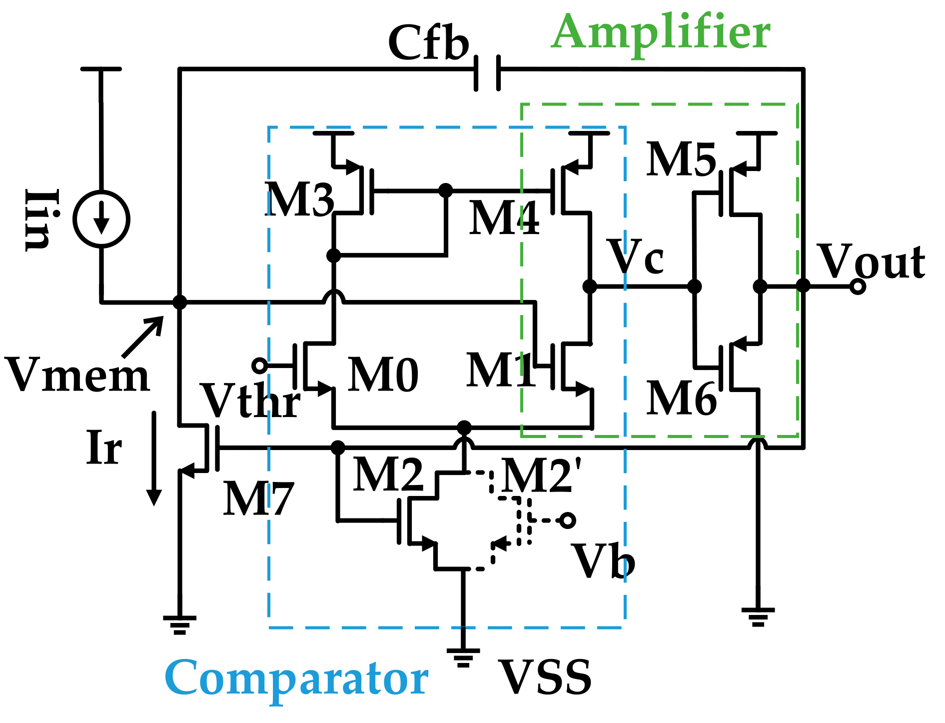
Based on the operation principle of the neuron, the new designed artificial neuron is shown in
Figure 5. In the design, the adjustable voltage threshold is adopted. With the current charging, I
in can inspire the artificial neuron to generate the mimicked spikes with a certain frequency with ultra-low power consumption.
The setting of the voltage threshold is achieved by combining the comparator and the traditional Axon-Hillock circuit. As shown in
Figure 5, the inverter with the two devices, M1 and M4, is the main part in the amplifier. At the same time, the inverter composed of M1 and M4 also operates in the comparator. The comparator with a mirror current source includes four transistors, M0, M1, M3 and M4.
With the positive input, the gate of M0 is the input of the reference threshold voltage V
thr. With the negative input, the gate of M1 is the input of the membrane voltage V
mem. When the voltage V
mem is higher than the threshold voltage V
thr, the comparator output voltage V
c is zero. Otherwise, when V
mem is lower than V
thr, V
c is set as V
dd. As the first stage inverter of the amplifier, M1 and M4 act as the same function as the inv1 of the Axon-Hillock in
Figure 3. Therefore, if V
mem is increased to be the threshold voltage V
thr, the output of the artificial neuron reaches a high level by the output of the second invertor. For the proposed circuit in
Figure 5, M1 and M4 are common-shared by the amplifier and the comparator. The common-shared design can effectively reduce the number of neuron circuits and therefore decrease the power consumption of the artificial neuron.
The power consumption is the key factor to be considered in the artificial neuron design [
22]. To reduce the power consumption, one effective solution is to remove the membrane capacitor. As shown in
Figure 5, the parasitic capacitance in the negative half cycle of the comparator is used as a part of the capacitance. At the initial state, the output voltage V
out is zero. Therefore, the feedback capacitor C
fb can also be regarded as the membrane capacitor and charged by the input current I
in. The output voltage V
out is connected with the gate of M7. Therefore, M7 is not only a switch of the reset current I
r, but also the current source of I
r.
To further reduce the power consumption, the tail current source of the comparator is effectively processed. In general, the offset voltage of the tail current source M2′ is provided by the reference voltage Vb. However, the branch of M2′, M0 and M3 is always at the conduction state because of the existence of Vthr and Vb. In this situation, the quiescent current always exists even without the input current. Therefore, the neural circuit still has a large amount of power loss during the sleeping state. To solve the problem, Vb is not used anymore.
As shown in
Figure 5, the actual bias of the M2 is provided by the output voltage V
out of the artificial neuron. When there is no input current, V
out is zero and there i no static current through M2. The reduction of the tail current of the comparator can effectively decrease the power consumption. The operation process of the artificial neuron is shown in
Figure 6. At the initial state, there is no light irritation. The output of the photodiode is zero. Therefore, the input current I
in is also zero without the light irritation. The membrane voltage V
mem is at a low level, which is lower than the threshold voltage V
thr. Therefore, the output voltage is low. No reset current is generated because the transistor M7 is at the off-state. As the input increases, Tr also shrinks, and the frequency of the output spike becomes higher.
When the light is switched on, the dc current Iin is produced by the photodiode. The capacitor Cfb is charged by Iin. Therefore, the membrane voltage Vmem is increased during the charging process. Before Vmem reaches the threshold voltage, the output voltage of the neural circuit Vout is kept at a low level. When Vmem exceeds Vthr, the Vc of the first stage inverter is switched to a low level quickly. Meanwhile, Vout of the second inverter is quickly changed from 0 to Vdd. The membrane voltage Vmem is pulled up to the level of Vout by the feedback capacitor to maintain the stable state of the comparator and the invertors. As Vout rises, the reset current source M7 is turned on and generates the reset current Ir. Because Ir is greater than the input current Iin, the membrane voltage Vmem decreases back to the threshold voltage Vthr. Thus, the output voltage of the comparator and artificial neuron are reset to their initial state. The re-closed reset current source M7 causes the feedback capacitor to be charged by input current again.
The rest time Tr is controlled by the input current, the feedback capacitance and the threshold voltage at the same time. The resting time is inversely proportional to the input current Iin, but proportional to the feedback capacitance Cfb and the reference voltage Vthr.
4. Result and Discussions
The proposed circuit is simulated with SMIC 40 nm CMOS process. The sizes of the transistors in the circuit are shown in
Figure 7. In order to reduce the leakage currents of the transistors and suppress the static power consumption of the circuit, the channel length of M7 is set to 120 nm. The feedback capacitor Cfb is set to 5 fF. The power supply voltage is set to 500 mV and the reference voltage Vthr to 50 mV. The default value of the input current Iin is 5 pA.
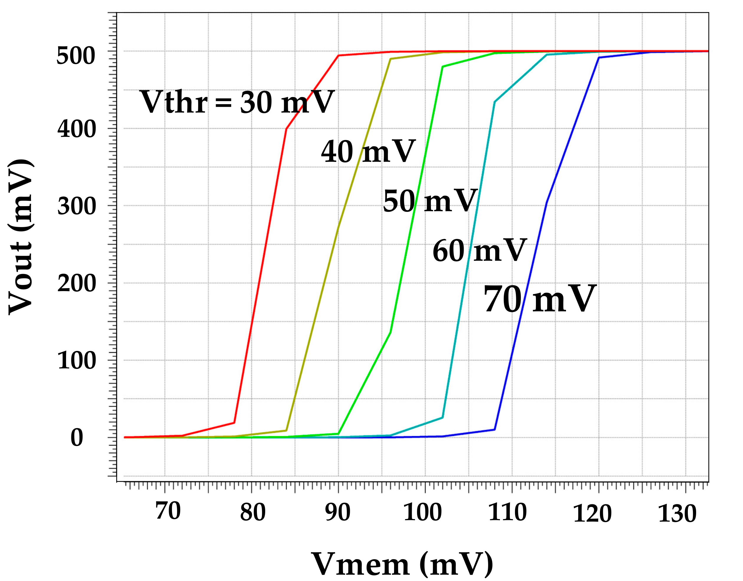
Figure 8 shows the relationship between the output voltage V
out and the membrane voltage V
mem with different reference voltages V
thr. In the figure, the value of V
thr is varied from 30 mV to 70 mV. It can be seen that the flip point of the output is changed from 80 mV to 110 mV corresponding to the different V
thr values. This means that the reference voltage of the comparator has a proportional effect on the flipping point of the output, while the traditional one depends entirely on the process parameters of the inverter [
14,
15,
16]. Adoption of the comparator reduces the influence of process parameters on the circuit flipping mechanism and improves the robustness of the circuit [
10]. The sweep simulation with Vthr varied from 0 to 100 mV is conducted and the same tendency can be obtained, showing the circuit to have a wide operating range.
As illustrated in
Figure 5, the tail current of the comparator is cut off by the gate control on M2. The gate of M2 is directly connected with the output voltage. At this point, except for the weak leakage current of M3 and M7, there are no static currents on the other MOS transistors in the neural circuit. The static power consumption can be suppressed effectively. When the input current is not 0, the tail current source M2 is turned on by V
out, providing the current for the comparator. When V
mem exceeds V
thr, the two branches of the comparator are all switched on. All of the transistors in the neural circuit except M6 and M7 have current flowing through.
The total power consumption of the neural circuit and the energy loss by a spike signal in the range of input current from 1 to 150 pA are shown in
Figure 9a. The power P is the product of the supply voltage V
dd and the DC current. E denotes the energy consumption per spike. With the increment of I
in, the charging speed of the feedback capacitor and the frequency of the state are accelerated. The minimum power is 35 pW with the input current 5 pA. The energy consumed by a spike is as low as 3 fJ. The cycle period is shrunk with the increasing of the input current I
in. In the tradeoff of the cycle time, the energy consumed by a spike signal is decreased, being opposite to the increment of the circuit power.
As shown in
Figure 9b, the frequency of the spike signal is positively correlated with the input current. As the input current increases, the charging speed of the current on the feedback capacitor increases, which can significantly reduce the charging time of the membrane voltage. With the intensity of the input signal triggering the circuit, the output spike signal of the corresponding frequency is generated, which is the artificial neural source that imitates the working mechanism of the biological neuron, and it is also the core of the SNN signal encoding.
As shown in
Figure 10, the artificial neurons in different schemes of the tail current sources (with M2 or with M2′) are compared in terms of the power consumption. The voltage offset of the tail current source of M2 is connected directly with the output voltage V
out. The tail current source consisting of M2′ is provided with a voltage offset by a separate voltage source. It can be seen, in
Figure 10a, that the power consumption in the activated state of the V
out-biased tail current source (with M2) is significantly lower than that of the fixed-biased tail current source (with M2′). Similarly in
Figure 10b, the power consumed by each spike in the circuit using the V
out-bias current source M2 is also reduced.
The neuron unit in SNN is not activated during the iterations, so the power consumption in the standby state accounts for the main part of the total power consumption. When the input current is 0, the DC current is 6.5 pA, which means a standby power consumption of 3.25 pw. However, if a fixed-biased tail current source M2′ is used, the DC current in the standby state increases to 80 pA due to the presence of the on-state current, which means a static power consumption of 40 pW. This is intolerable in a low-power neuron circuit. The use of a Vout-biased tail current source significantly reduces the overall power consumption of the circuit.
In order to verify the influence of the supply voltage V
dd and ambient temperature on the working frequency, the circuits are verified under the conditions of the feedback capacitance of 5 fF and the input current of 40 pA [
20]. As shown in
Figure 11a, with the increase of the power supply voltage V
dd, the emission frequency decreases. With the voltage range of 0.44–0.56 V, the variation of the frequency is approximately 1.5%. This means that the circuit is less affected by the power supply ripple and that the circuit is robust to the potential power supply voltage noise. The relationship between the firing frequency and the temperature is shown in
Figure 11b. With the temperature increasing, the firing frequency tends to increase. The maximum variation of the emission frequency is approximately 6% in the range of 27–41 °C.
The transient state simulation results of the neural circuits are shown in
Figure 12. When the input current I
in is zero, the membrane voltage V
mem and the output of the artificial neuron remain at zero. When the input current is 5 pA (I
in in
Figure 10), V
mem is increased with the charging by the input current. Afterwards, by the presence of the reset current source M7, V
mem is decreased. In this way, the spikes with certain frequency can be generated, as shown by the Vout result in
Figure 12.
Figure 13 shows the layout of the designed neuron circuit. Thanks to the shrinking process size, its area is only 13 μm
2, which makes it easy to implement the integration of the neuron arrays with thousands of the retina cells.
The designed retinal circuit is fabricated based on standard CMOS 40-nm technology.
Figure 14 shows the input and output waveforms of the retina with different input currents.
Figure 14a shows the input current waveform. After the artificial retina processing, the output voltage is shown in
Figure 14b. As the input changes from 6.3 pA to 9.4 pA, the interval between output spikes changes from 0.27 ms to 0.19 ms, that is, the frequency changes from 3.7 kHz to 5.3 kHz. For the performance of the fabricated chip, when the working voltage is 500 mV, the overall power consumption is 23 μW, which is mainly consumed by the reference voltage part. With the input current of 5 pA, and the temperature changing from 25 °C to 40 °C, the output spike frequency is varied within 2.3%. When the supply voltage is varied from 440 mV to 550 mV, the maximum output spike frequency is changed within 7.4%. The artificial neuron circuit can generate the spikes with the frequency ranging from 0.8–80 kHz when the input current is changed from 1 pA to 150 pA. It can be seen that the measured result coincides with the simulated ones.
To get a clear comparison with the other similar published works,
Table 1 lists the key results of the designed circuit and the other published works. The results in the paper show better performance, especially in terms of the ultra-low power consumption. The power consumption of the design in the paper is approximately 35 pW, which is compatible with the result in [
18]. In [
18], the power supply voltage is 200 mV, while the voltage in this paper is 500 mV. The layout area of the design is also smaller than those of the other published results. Besides the low power consumption of the design, the robustness of the circuit is the other advantage. For [
18], both the capacitor C
mem and the comparator are removed to obtain the low power consumption, with the sacrifice of the robustness of the circuit.
The adopted comparator can improve the stability of the circuit. The stability is an important parameter for the neurons used in the network. In a circuit without a comparator, the flip threshold is determined by the threshold of the MOS transistor itself, which is easily affected by the PTV variables. For example, the circuit in [
18] is more susceptible to PVT factors without using a comparator. In the simulation results, the spike frequency fluctuates up to 20% by the temperature and up to 25% by the supply voltage. For the circuit in the paper, the fluctuation is controlled successfully within 6% by the temperature and within 1.5% by the voltage. It can be seen that the circuit in the paper can improve the temperature fluctuation by three times and the voltage fluctuation by 16 times when it is compared with [
18].


