
A 320 μW Multi-Band Receiver with N-Path Switched-Capacitor Networks


Abstract
:1. Introduction
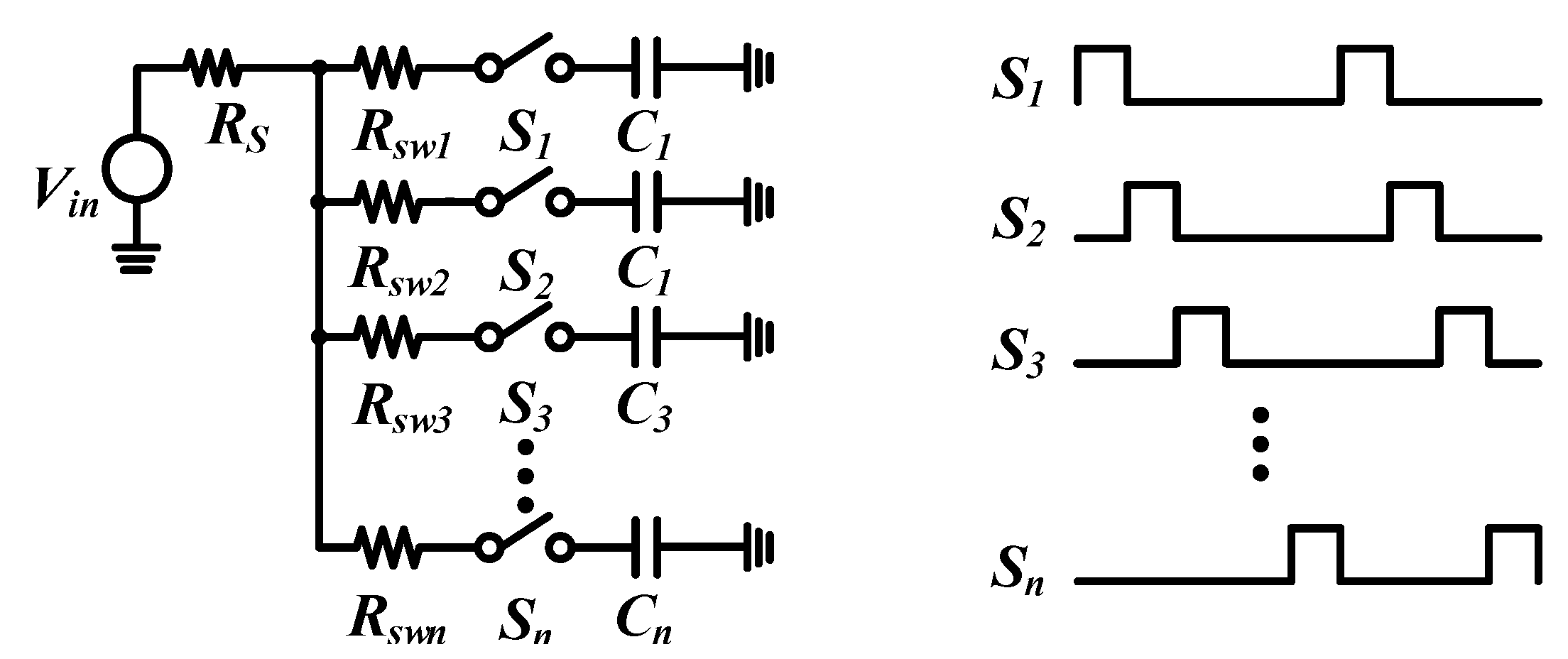
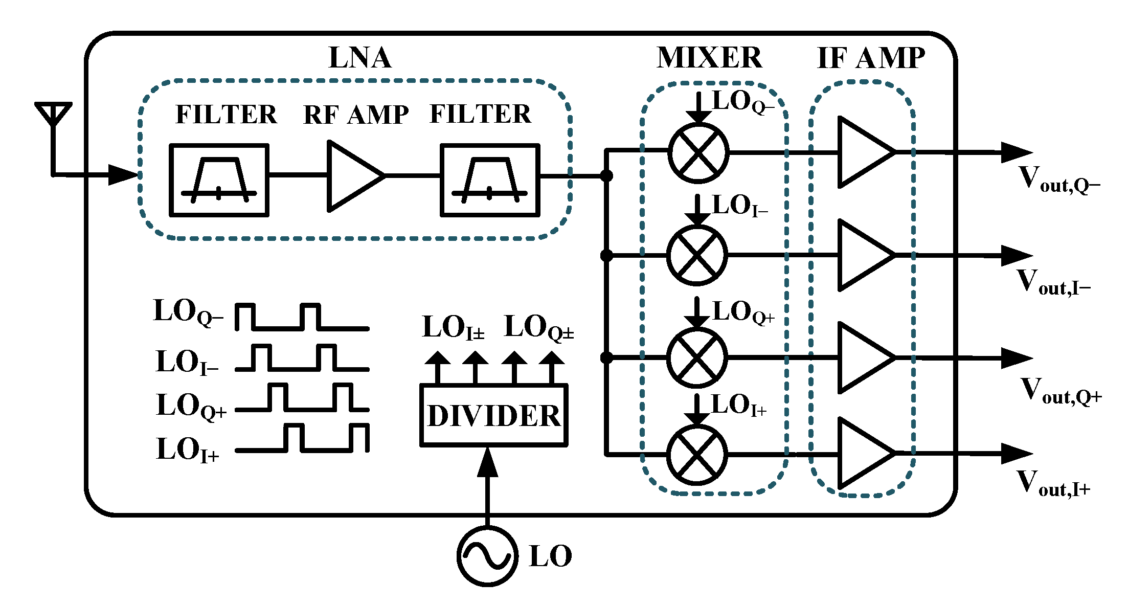
2. ULP Receiver with NPSC Networks
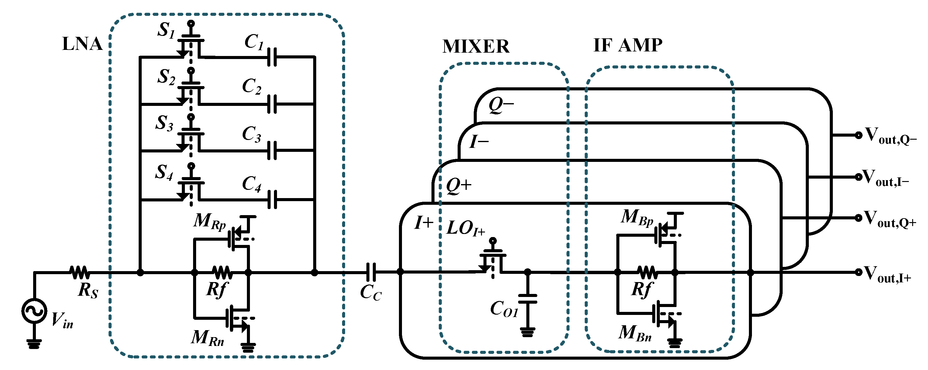
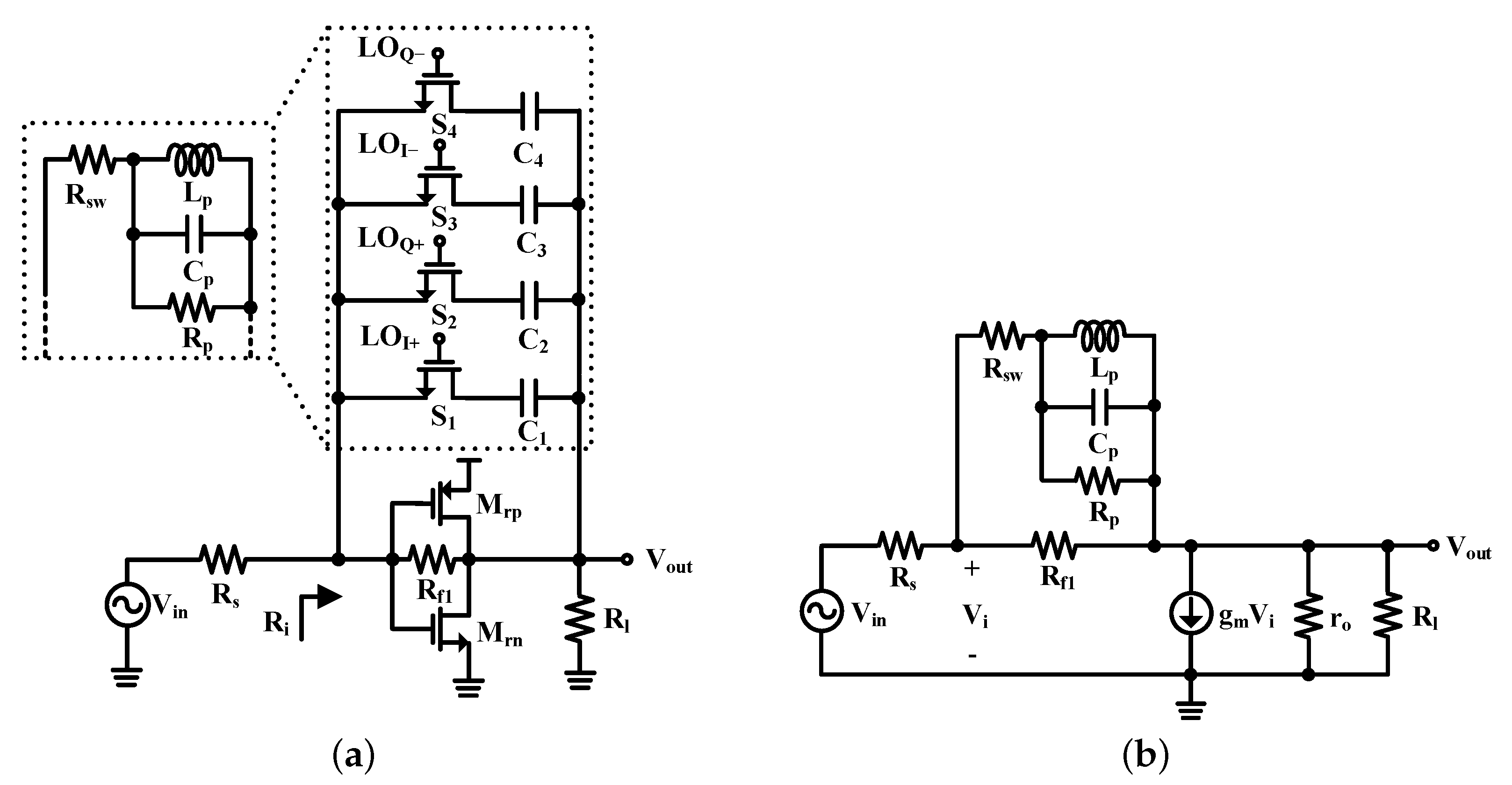
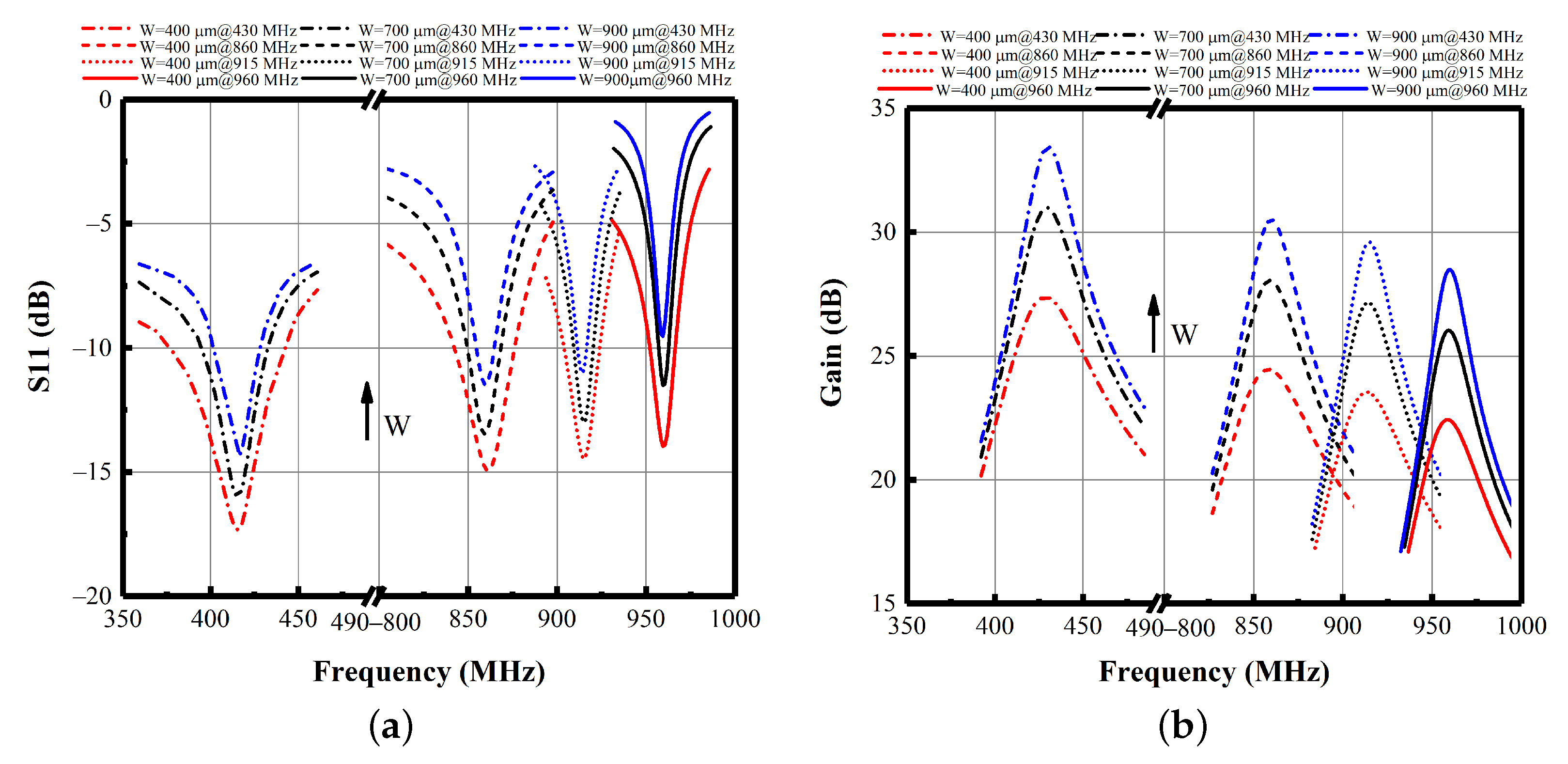
2.1. LNA with an NPSC Network
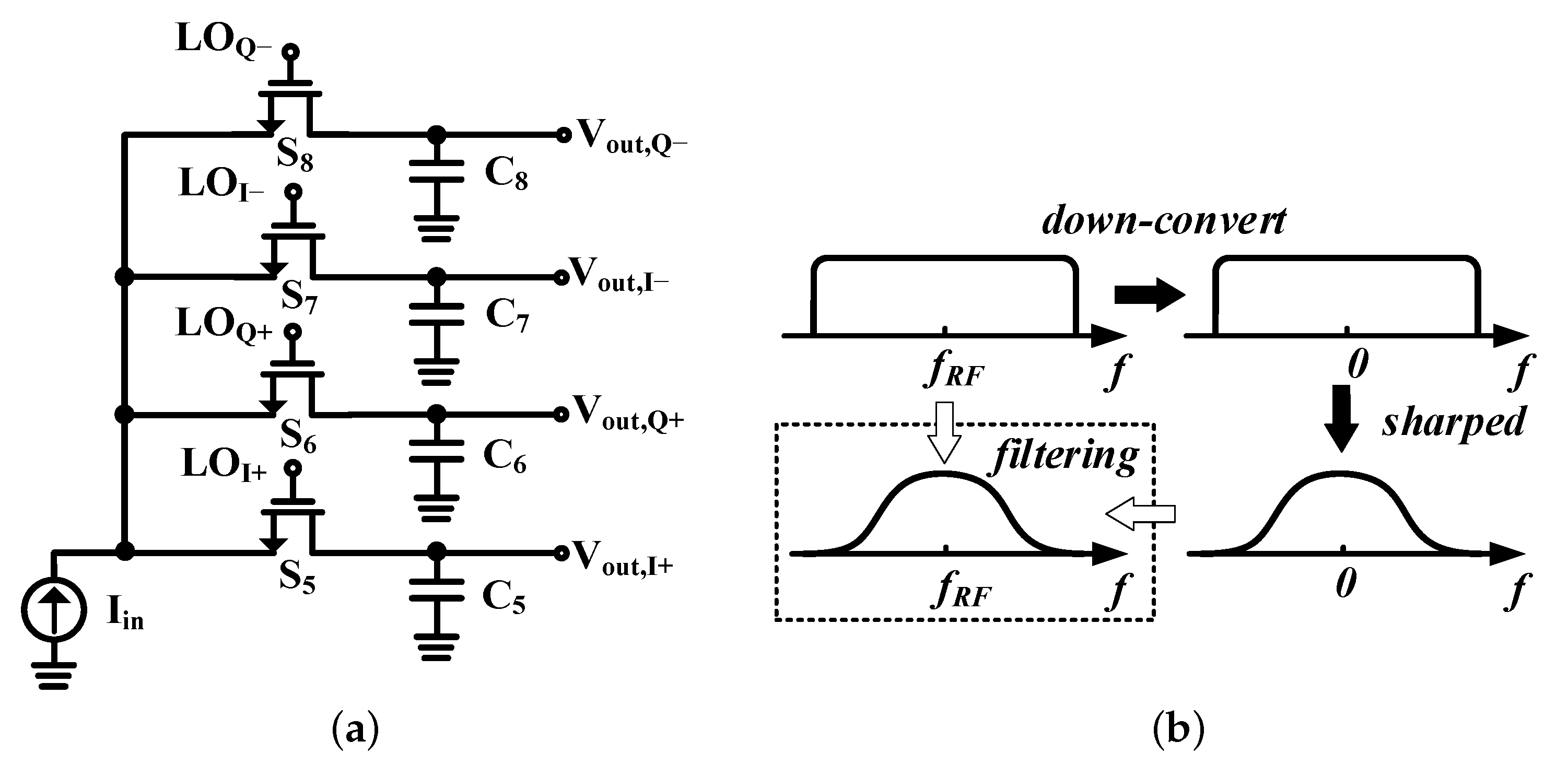
2.2. NPSC Mixer
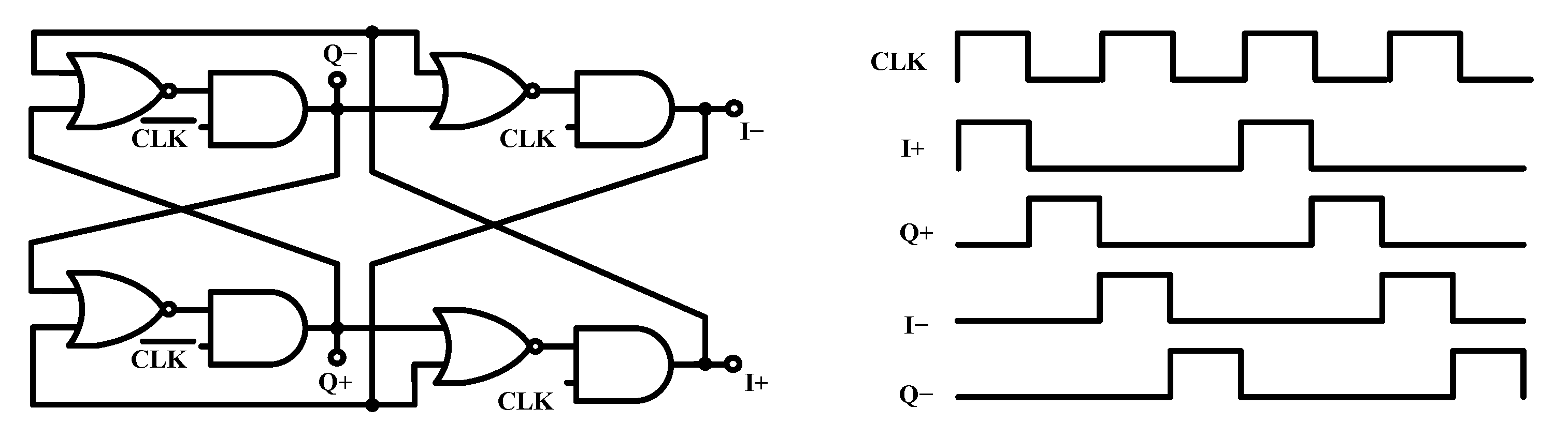
2.3. Divider
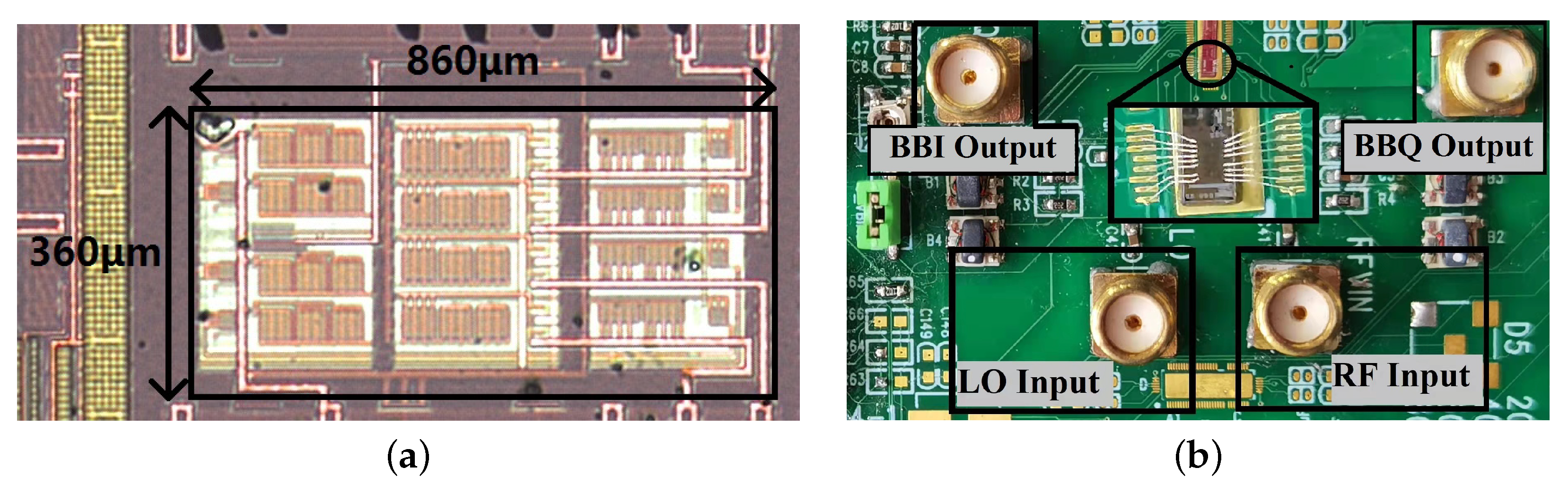
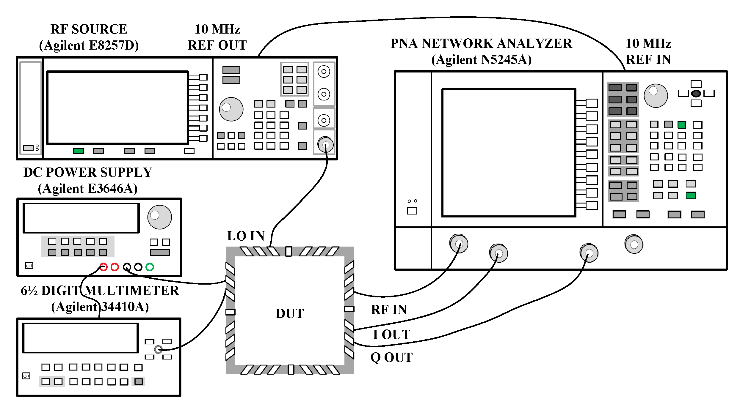
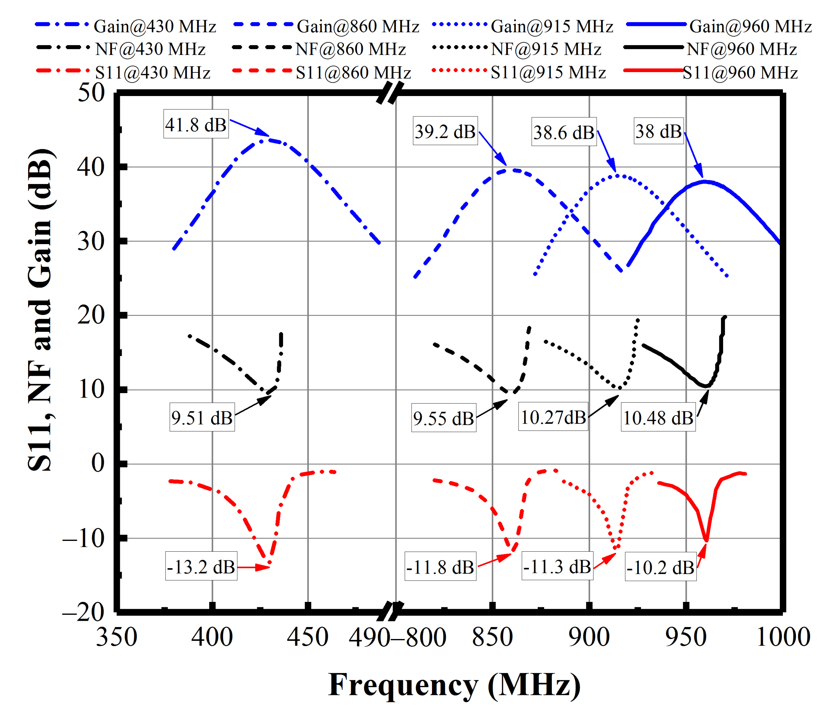
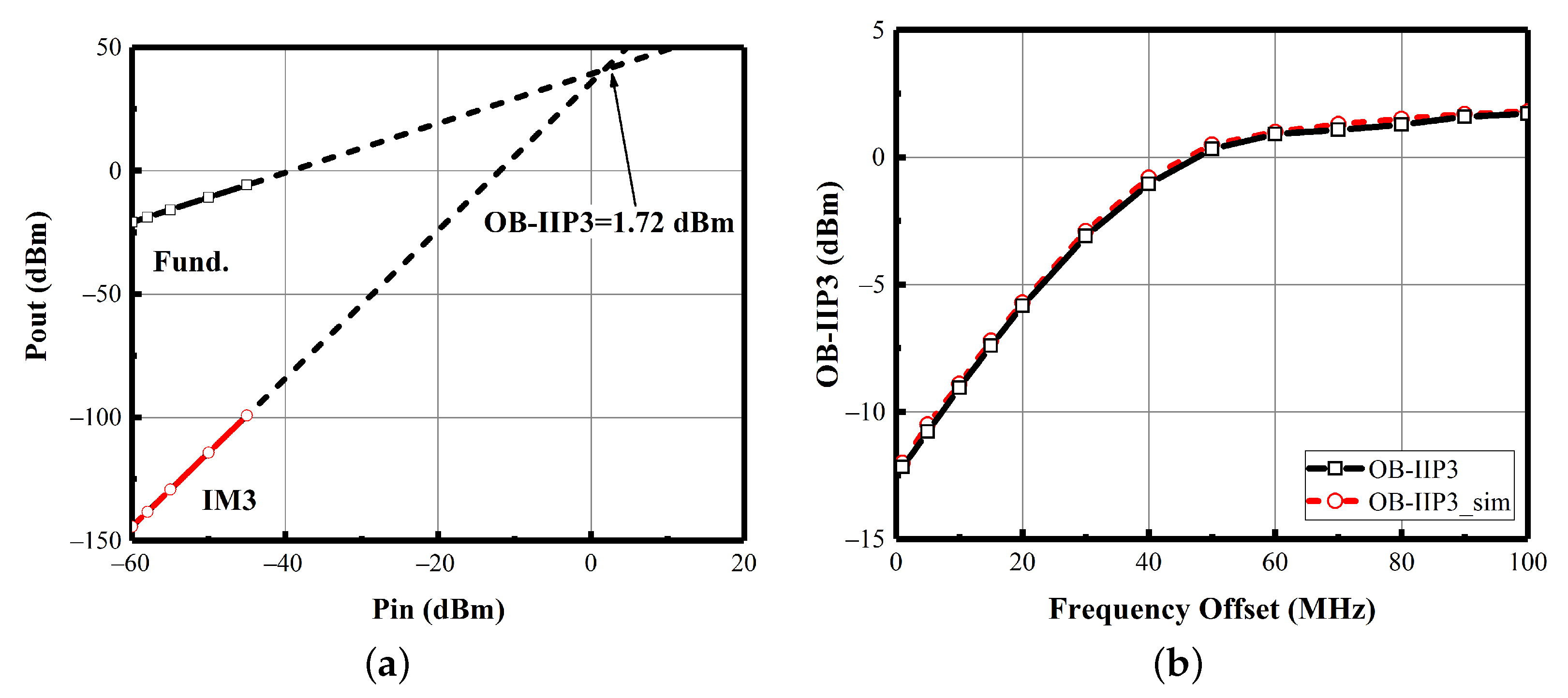
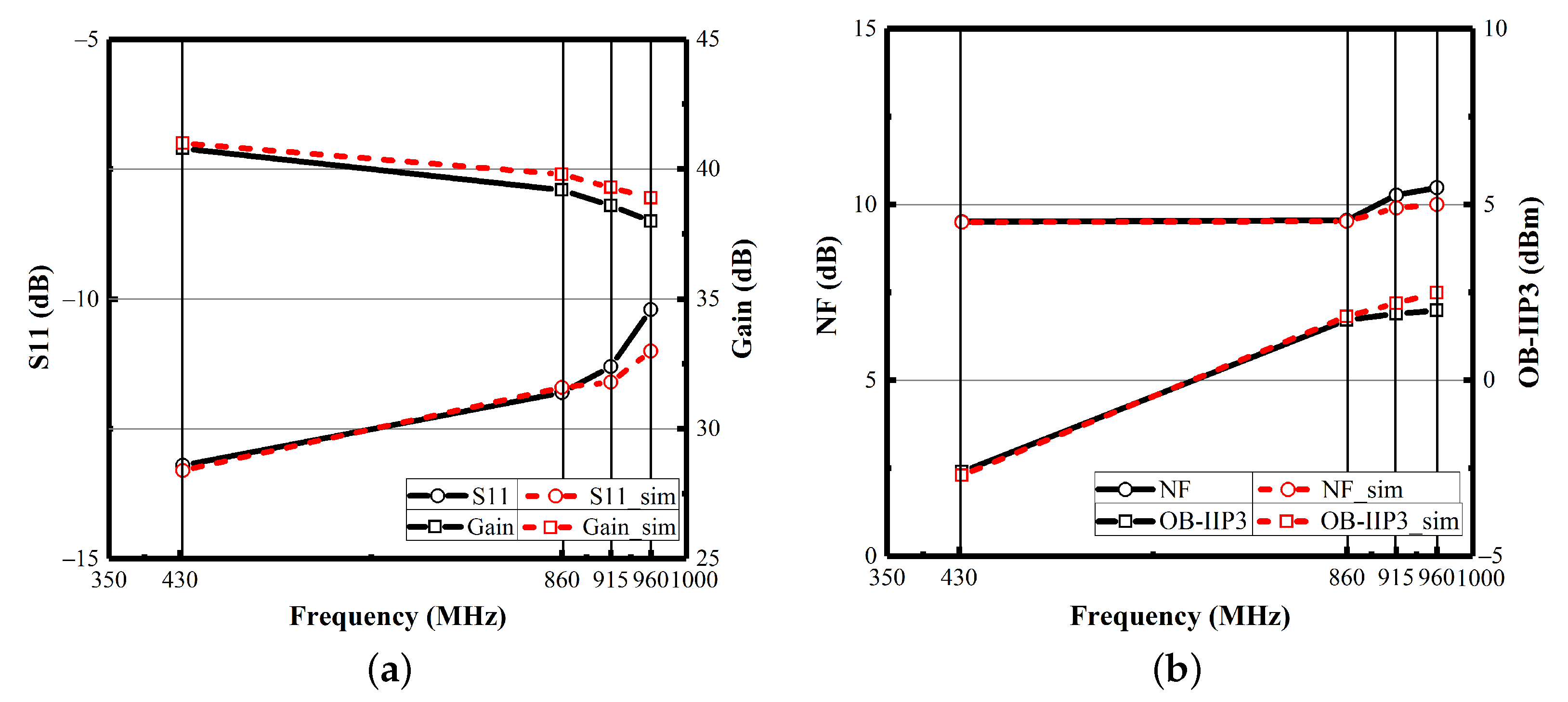
3. Measurement Results
4. Conclusions
Author Contributions
Funding
Conflicts of Interest
Abbreviations
| ULP | Ultra-low power |
| NPSC | N-path switched-capacitor |
| LNA | Low noise amplifier |
| IoT | Internet of Things |
| LPTV | Linear periodically time-variant |
| FoM | Figure of merit |
References
- Wang, K.; Qiu, L.; Koo, J.; Ruby, R.; Otis, B. Design of 1.8-mW PLL-Free 2.4-GHz Receiver Utilizing Temperature-Compensated FBAR Resonator. IEEE J. Solid-State Circuits 2018, 53, 1628–1639. [Google Scholar] [CrossRef]
- Park, B.; Kwon, K. 2.4-GHz Bluetooth Low Energy Receiver Employing New Quadrature Low-Noise Amplifier for Low-Power Low-Voltage IoT Applications. IEEE Trans. Microw. Theory Tech. 2021, 69, 1887–1895. [Google Scholar] [CrossRef]
- Tamura, M.; Takano, H.; Shinke, S.; Fujita, H.; Nakahara, H.; Suzuki, N.; Nakada, Y.; Shinohe, Y.; Etou, S.; Katayama, Y.; et al. 30.5 A 0.5 V BLE Transceiver with a 1.9 mW RX Achieving 96.4 dBm Sensitivity and 4.1 dB Adjacent Channel Rejection at 1 MHz Offset in 22 nm FDSOI. In Proceedings of the 2020 IEEE International Solid- State Circuits Conference-(ISSCC), San Francisco, CA, USA, 16–20 February 2020; pp. 468–470. [Google Scholar]
- Barzgari, M.; Ghafari, A.; Meghdadi, M.; Medi, A. A Current Re-Use Quadrature RF Receiver Front-End for Low Power Applications: Blixator Circuit. IEEE J. Solid-State Circuits 2022, 57, 2672–2684. [Google Scholar] [CrossRef]
- Sun, Z.; Liu, H.; Huang, H.; Tang, D.; Xu, D.; Kaneko, T.; Li, Z.; Pang, J.; Wu, R.; Okada, K.; et al. A 0.85 mm2 BLE Transceiver Using an On-Chip Harmonic-Suppressed RFIO Circuitry With T/R Switch. IEEE Trans. Circuits Syst. I Regul. Pap. 2021, 68, 196–209. [Google Scholar] [CrossRef]
- Lei, K.; Mak, P.; Law, M.; Martins, R.P. A regulation-free sub-0.5 V 16/24 MHz crystal oscillator for energy-harvesting BLE radios with 14.2 nJ startup energy and 31.8 pW steady-state power. In Proceedings of the 2018 IEEE International Solid-State Circuits Conference-(ISSCC), San Francisco, CA, USA, 11–15 February 2018; pp. 52–54. [Google Scholar]
- Lin, L.; Jain, S.; Alioto, M. Integrated Power Management for Battery-Indifferent Systems With Ultra-Wide Adaptation Down to nW. IEEE J. Solid-State Circuits 2020, 55, 967–976. [Google Scholar] [CrossRef]
- Liu, L.; Xing, Y.; Huang, W.; Liao, X.; Li, Y. A 10 mV–500 mV Input Range, 91.4% Peak Efficiency Adaptive Multi-Mode Boost Converter for Thermoelectric Energy Harvesting. IEEE Trans. Circuits Syst. I Regul. Pap. 2022, 69, 609–619. [Google Scholar] [CrossRef]
- Liu, Z.; Tan, Y.; Li, H.; Jiang, H.; Liu, J.; Liao, H. A 0.5-V 3.69-nW Complementary Source-Follower-C Based Low-Pass Filter for Wearable Biomedical Applications. IEEE Trans. Circuits Syst. I Regul. Pap. 2020, 67, 4370–4381. [Google Scholar] [CrossRef]
- Tamura, M.; Takano, H.; Nakahara, H.; Fujita, H.; Arisaka, N.; Shinke, S.; Suzuki, N.; Nakada, Y.; Nakada, Y.; Shinohe, Y.; et al. A 0.5 V BLE Transceiver With a 1.9-mW RX Achieving 96.4 dBm Sensitivity and 27 dBm Tolerance for Intermodulation From Interferers at 6 and 12 MHz Offsets. IEEE J. Solid-State Circuits 2020, 55, 3376–3386. [Google Scholar] [CrossRef]
- Zhang, F.; Wang, K.; Koo, J.; Miyahara, Y.; Otis, B. A 1.6 mW 300 mV supply 2.4 GHz receiver with 94 dBm sensitivity for energy-harvesting applications. In Proceedings of the 2013 IEEE International Solid-State Circuits Conference Digest of Technical Papers, San Francisco, CA, USA, 17–21 February 2013; pp. 456–457. [Google Scholar]
- Im, J.; Breiholz, J.; Li, S.; Calhoun, B.; Wenzloff, D.D. A Fully Integrated 0.2 V 802.11 ba Wake-Up Receiver with −91.5 dBm Sensitivity. In Proceedings of the IEEE Radio Frequency Integrated Circuits Symposium (RFIC), Los Angeles, CA, USA, 4–6 August 2020; pp. 339–342. [Google Scholar]
- Yi, H.; Yu, W.; Mak, P.; Yin, J.; Martins, R.P. A 0.18 V 382 μW Bluetooth Low-Energy Receiver Front-End With 1.33 nW Sleep Power for Energy-Harvesting Applications in 28 nm CMOS. IEEE J. Solid-State Circuits 2018, 53, 1618–1627. [Google Scholar] [CrossRef]
- Tan, G.H.; Ramiah, H.; Mak, P.-I.; Martins, R.P. A 0.35 V 520 μW 2.4 GHz Current-Bleeding Mixer With Inductive-Gate and Forward-Body Bias, Achieving >13 dB Conversion Gain and >55 dB Port-to-Port Isolation. IEEE Trans. Microw. Theory Tech. 2017, 65, 1284–1293. [Google Scholar] [CrossRef]
- Elsayed, O.; Abouzied, M.; Vaidya, V.; Ravichandran, K.; Sánchez-Sinencio, E. An Ultralow-Power RF Wireless Receiver With RF Blocker Energy Recycling for IoT Applications. IEEE Trans. Microw. Theory Tech. 2018, 66, 4927–4942. [Google Scholar] [CrossRef]
- Wang, P.H.P.; Mercier, P.P. An Interference-Resilient BLE-Compatible Wake-Up Receiver Employing Single-Die Multi-Channel FBAR-Based Filtering and a 4-D Wake-Up Signature. IEEE J. Solid-State Circuits 2021, 56, 416–426. [Google Scholar] [CrossRef]
- Ye, D.; Xu, R.; Shi, C.-J.R. A Nonlinear Receiver Leveraging Cascaded Inverter-Based Envelope-Biased LNAs for In-Band Interference Suppression in the Amplitude Domain. IEEE J. Solid-State Circuits 2021, 56, 3360–3374. [Google Scholar] [CrossRef]
- Han, G.; Kinget, P.R. Double-Conversion, Noise-Cancelling Receivers Using Modulated LNTAs and Double-Layer Passive Mixers for Concurrent Signal Reception With Tuned RF Interface. IEEE Trans. Circuits Syst. I Regul. Pap. 2021, 68, 3913–3926. [Google Scholar] [CrossRef]
- Bhat, A.N.; van der Zee, R.A.R.; Nauta, B. A Baseband-Matching-Resistor Noise-Canceling Receiver With a Three-Stage Inverter-Only OpAmp for High In-Band IIP3 and Wide IF Applications. IEEE J. Solid-State Circuits 2021, 56, 1994–2006. [Google Scholar] [CrossRef]
- Purushothaman, V.K.; Klumperink, E.A.M.; Clavera, B.T.; Nauta, B. A Fully Passive RF Front End with 13 dB Gain Exploiting Implicit Capacitive Stacking in a Bottom-Plate N-Path Filter/Mixer. IEEE J. Solid-State Circuits 2020, 55, 1139–1150. [Google Scholar] [CrossRef] [Green Version]
- Khorshidian, M.; Krishnaswamy, H. 26.7 An Impedance-Transforming N-Path Filter Offering Passive Voltage Gain. In Proceedings of the 2021 IEEE International Solid- State Circuits Conference (ISSCC), San Francisco, CA, USA, 13–22 February 2021; pp. 365–367. [Google Scholar]
- von Grunigen, D.C.; Sigg, R.P.; Schmid, J.; Moschytz, G.S.; Melchior, H. An integrated CMOS switched-capacitor bandpass filter based on N-path and frequency-sampling principles. IEEE J. Solid-State Circuits 1983, 18, 753–761. [Google Scholar] [CrossRef]
- Lin, Z.; Mak, P.-I.; Martins, R.P. A Sub-GHz Multi-ISM-Band ZigBee Receiver Using Function-Reuse and Gain-Boosted N-Path Techniques for IoT Applications. IEEE J. Solid-State Circuits 2014, 49, 2990–3004. [Google Scholar] [CrossRef]
- Agrawal, A.; Natarajan, A. An Interferer-Tolerant CMOS Code-Domain Receiver Based on N-Path Filters. IEEE J. Solid-State Circuits 2018, 53, 1387–1397. [Google Scholar] [CrossRef]
- Zolkov, E.; Ginzberg, N.; Cohen, E. A 1–2 GHz Quadrature Balanced N-Path Receiver for Frequency Division Duplex Systems. IEEE Trans. Microw. Theory Tech. 2022, 70, 597–610. [Google Scholar] [CrossRef]
- Lee, D.; Kwon, K. CMOS Channel-Selection LNA with a Feedforward N-Path Filter and Calibrated Blocker Cancellation Path for FEM-Less Cellular Transceivers. IEEE Trans. Microw. Theory Tech. 2022, 70, 1810–1820. [Google Scholar] [CrossRef]
- Ying, R.; Molnar, A. Impedance Transparency and Performance Metrics of HBT-Based N-Path Mixers for mmWave Applications. IEEE Trans. Circuits Syst. I Regul. Pap. 2021, 68, 2210–2223. [Google Scholar] [CrossRef]
- Salazar, C.; Cathelin, A.; Kaiser, A.; Rabaey, J. A 2.4 GHz Interferer-Resilient Wake-Up Receiver Using A Dual-IF Multi-Stage N-Path Architecture. IEEE J. Solid-State Circuits 2016, 51, 2091–2105. [Google Scholar] [CrossRef]
- Lin, F.; Mak, P.; Martins, R. 3.9 An RF-to-BB current-reuse wideband receiver with parallel N-path active/passive mixers and a single-MOS pole-zero LPF. In Proceedings of the 2014 IEEE International Solid-State Circuits Conference Digest of Technical Papers (ISSCC), San Francisco, CA, USA, 9–13 February 2014; pp. 74–75. [Google Scholar]
- Klumperink, E.A.M.; Westerveld, H.J.; Nauta, B. N-path filters and mixer-first receivers: A review. In Proceedings of the 2017 IEEE Custom Integrated Circuits Conference (CICC), Austin, TX, USA, 30 April 2017–3 May 2017; pp. 1–8. [Google Scholar]
- Bialek, H.; Binaie, A.; Ahasan, S.; Sadagopan, K.R.; Johnston, M.L.; Krishnaswamy, H.; Natarajan, A. A Passive Wideband Noise-Canceling Mixer-First Architecture With Shared Antenna Interface for Interferer-Tolerant Wake-Up Receivers and Low-Noise Primary Receivers. IEEE J. Solid-State Circuits 2022, 57, 2611–2625. [Google Scholar] [CrossRef]
- Ghaffari, A.; Klumperink, E.A.M.; Soer, M.C.M.; Nauta, B. Tunable High-Q N-Path Band-Pass Filters: Modeling and Verification. IEEE J. Solid-State Circuits 2011, 46, 998–1010. [Google Scholar] [CrossRef] [Green Version]
- Hameed, S.; Pamarti, S. Impedance Matching and Reradiation in LPTV Receiver Front-Ends: An Analysis Using Conversion Matrices. IEEE Trans. Circuits Syst. I Regul. Pap. 2018, 65, 2842–2855. [Google Scholar] [CrossRef]
- Zolkov, E.; Cohen, E. Analysis and Modeling of N-Path Circuits Peak Frequency Shift Caused by Switch Parasitics. IEEE Trans. Circuits Syst. II Express Briefs 2022, 69, 374–378. [Google Scholar] [CrossRef]
- Zolkov, E.; Cohen, E. Analysis of the Effect of Switch Parasitic Resistance and Capacitance on N-Path Filters Using State Space Representation. IEEE Trans. Circuits Syst. II Express Briefs 2020, 67, 1889–1893. [Google Scholar] [CrossRef]
- Reiskarimian, N.; Khorshidian, M.; Krishnaswamy, H. Inductorless, Widely Tunable N-Path Shekel Circulators Based on Harmonic Engineering. IEEE J. Solid-State Circuits 2021, 56, 1425–1437. [Google Scholar] [CrossRef]
- Lin, Z.; Mak, P.; Martins, R.P. Analysis and Modeling of a Gain-Boosted N-Path Switched-Capacitor Bandpass Filter. IEEE Trans. Circuits Syst. I Regul. Pap. 2014, 61, 2560–2568. [Google Scholar] [CrossRef]
- Krishnamurthy, S.; Maksimovic, F.; Iotti, L.; Niknejad, A.M. Analysis and Design of Submilliwatt Interference-Tolerant Receivers Leveraging N-Path Filter-Based Translational Positive Feedback. IEEE Trans. Microw. Theory Tech. 2021, 69, 3496–3509. [Google Scholar] [CrossRef]
- Lee, S.; Choi, I.; Kim, H.; Kim, B. A Sub-mW Fully Integrated Wide-Band Receiver for Wireless Sensor Network. IEEE Microw. Wirel. Compon. Lett. 2015, 25, 319–321. [Google Scholar] [CrossRef]
- Zhiqun, L.; Yao, Y.; Zengqi, W.; Guoxiao, C.; Luo, L. A 1V 1.4 mW multi-band ZigBee receiver with 64 dB SFDR. Microelectron. J. 2018, 76, 43–51. [Google Scholar]
- Kargaran, E.; Bryant, C.; Manstretta, D.; Strange, J.; Castello, R. A Sub 0.6 V, 330 μW, 0.15 mm2 Receiver Front-End for Bluetooth Low Energy (BLE) in 22 nm FD-SOI with Zero External Components. In Proceedings of the 2019 IEEE Asian Solid-State Circuits Conference (A-SSCC), Macau, China, 4–6 November 2019; pp. 169–172. [Google Scholar]
- Rekhi, A.S.; Arbabian, A. 14.5 mm2 8 nW −59.7 dBm-sensitivity ultrasonic wake-up receiver for power-, area-, and interference-constrained applications. In Proceedings of the 2018 IEEE International Solid State Circuits Conference (ISSCC), San Francisco, CA, USA, 11–15 February 2018; pp. 454–456. [Google Scholar]


| Block | Power Consumption | Power Contribution |
|---|---|---|
| LNA | 134 W | 42% |
| IF amplifier | 134 W | 42% |
| Divider | 52 W | 16% |
| Total | 320 W | 100% |
| Reference | [1] | [38] | [39] | [40] | [41] | This Work |
|---|---|---|---|---|---|---|
| Tech./nm | 65 | 28 | 28 | 180 | 22 | 90 |
| Freq./MHz | 2400 | 2200–2400 | 850–2550 | 780/868/915 | 2400 | 430/860/915/960 |
| Power/W | 860 | 580 | 530–970 | 1420 | 330 | 320 |
| VDD/V | 1 | 1 | 0.8 | 1 | 0.55 | 0.4 |
| Gain/dB | 57.8 | 19–42 | 55 | 45.9 | 32.3 | |
| NF/dB | 15.7 | 11.6 | 13.6 | 8.5 | 9.4 | |
| OB-IIP3/dBm | −13.4 | 3.3 | −7.5 | −33.5 1 | −8 | |
| Area/mm | 0.45 | – | 0.17 | 1.41 | 0.15 | 0.31 |
| Sensitivity/dBm | −88.3 | −96.4 | −90.4 | −102 | −89.6 | |
| FoM/dB2 | 86.6 | – | 76.4–81.6 | 82.5 | 72.5 |
Publisher’s Note: MDPI stays neutral with regard to jurisdictional claims in published maps and institutional affiliations. |
© 2022 by the authors. Licensee MDPI, Basel, Switzerland. This article is an open access article distributed under the terms and conditions of the Creative Commons Attribution (CC BY) license (https://creativecommons.org/licenses/by/4.0/).
Share and Cite
Lei, L.; Han, F.; Liu, Z.; Qi, Q.; Wang, X.; Wang, W. A 320 μW Multi-Band Receiver with N-Path Switched-Capacitor Networks. Electronics 2022, 11, 4111. https://doi.org/10.3390/electronics11244111
Lei L, Han F, Liu Z, Qi Q, Wang X, Wang W. A 320 μW Multi-Band Receiver with N-Path Switched-Capacitor Networks. Electronics. 2022; 11(24):4111. https://doi.org/10.3390/electronics11244111
Chicago/Turabian StyleLei, Lei, Fang Han, Zicheng Liu, Quanwen Qi, Xinghua Wang, and Weijiang Wang. 2022. "A 320 μW Multi-Band Receiver with N-Path Switched-Capacitor Networks" Electronics 11, no. 24: 4111. https://doi.org/10.3390/electronics11244111