Article

A 177 ppm RMS Error-Integrated Interface for Time-Based Impedance Spectroscopy of Sensors

by
Antonio Vincenzo Radogna
1,2,*,
Simonetta Capone
1,
Luca Francioso
1,*,
Pietro Aleardo Siciliano
1 and
Stefano D’Amico
2
1
Institute for Microelectronics and Microsystems, National Research Council of Italy (CNR-IMM), Campus Ecotekne, Via per Monteroni s.n., 73100 Lecce, Italy
2
Department of Innovation Engineering, University of Salento, Campus Ecotekne, Via per Monteroni s.n., 73100 Lecce, Italy
*
Authors to whom correspondence should be addressed.
Electronics 2022, 11(22), 3807; https://doi.org/10.3390/electronics11223807
Submission received: 29 October 2022 / Revised: 15 November 2022 / Accepted: 17 November 2022 / Published: 19 November 2022

Abstract

:
This paper presents an integrated circuit for time-based electrical impedance spectroscopy (EIS) of sensors. The circuit exploits maximum-length sequences (MLS) in order to perform a broadband excitation of the sensors under test. Therefore, the measured time-domain EIS is obtained by cross-correlating the input with the output of the analog front end (AFE). Unlike the conventional digital approach, the cross-correlation operation is performed in the analog domain. This leads to a lower RMS error in the measured time-domain EIS since the signal processing is not affected by the quantization noise of the analog-to-digital converter (ADC). It also relaxes the sampling frequency of the ADC leading, along with the lack of random access memory (RAM) usage, to a reduced circuit complexity. Theoretical concepts about the circuit’s design and operation are presented, with an emphasis on the thermal noise phenomenon. The simulated performances are shown by testing a sensor’s equivalent model composed of a 50 kΩ resistor in parallel with a 100 p F capacitor. A time-based EIS output of 255 points was obtained with a maximum tested frequency of 500 k Hz and a simulated RMS error of 0.0177% (or 177 ppm).

1. Introduction

Impedance analysis instrumentation plays an important role in material development and characterization, biological research, and sensors’ read-outs. It is a valuable tool for investigating the electrical and physical parameters of matter and is also used to enhance the read-out performance in sensing applications [1]. Some examples of applications of impedance analysis are bioelectrical impedance (BioZ) measurement [2], electrical assessment of the cell metabolism [1], online built-in test for DC–DC converters [3], estimation of battery parameters due to aging [4], etc. In recent years, a plethora of electronic solutions for impedance analysis, both discrete component and integrated, have been presented [5] in order to accomplish the variety of requirements needed by the applications. Compared to discrete-component solutions, integrated circuits offer the advantage of overcoming the common accuracy issues of laboratory instrumentation [6]. Moreover, integrated solutions allow for the realization of miniaturized and portable analyzers, which are suitable for modern Internet-of-Things or point-of-care devices [5,7].
The most commonly implemented approach is synchronous detection (SD) [8], which consists of (1) a voltage-controlled current source (VCCS) for the stimulus injection between a pair of electrodes; (2) an instrumentation amplifier (IA) for signal preamplification; and (3) two multipliers for the extraction of the real parts (in-phase demodulation) and imaginary parts (quadrature demodulation) from the measured signal. This approach suffers from matching, offset, and synchronization issues between the stimulus and measuring subcircuits [6]. As an alternative, a self-mixing full-wave rectifier was used in [9] to implement a polar demodulation method. The magnitude and phase information were extracted, giving a simulated magnitude error of 0.3% with a max tested frequency of 1 M Hz . Information on the magnitude and phase of the impedance was also obtained through the system presented in [6] with a similar approach. The achieved measured error on the magnitude was 1.15% with a maximum tested frequency of 100 k Hz . In [10], an alternative approach based on ΔΣ demodulation was implemented achieving 15 bits of resolution and high temperature accuracy with a maximum working frequency of 16 k Hz . All these systems rely on single-tone sinusoids in order to perform the measurements, which exhibit the following drawback: the total measurement time resulting from the evaluation of multiple frequencies is the sum of the measurement times for each frequency. Moreover, the total time is limited by the minimum frequency used for the excitation.
Unlike sinusoids, which are narrow-band excitation signals, broadband signals can be used to stimulate the impedance under test in a wide frequency range while keeping a low total measurement time [2]. Popular signals used for broadband excitation are maximum-length sequences (MLS). These are pseudo-random binary signals with unique mathematical properties, thanks to which the impedance measurement can be performed in the time domain, requiring only the digital cross-correlation as a processing algorithm [5,11]. As an example, in [6] an MLS-based measurement circuit for bio-impedance spectroscopy was implemented. The system was able to measure 63 points (sixth-order MLS) with a maximum tested frequency of 125 k Hz , achieving a modest error performance of greater than 10% for the absolute resistor values.
In this paper, an integrated circuit for time-based impedance spectroscopy of sensors is presented. The circuit uses MLS-based signals for impedance analysis but unlike the conventional approach with digital cross-correlation, the signal processing is performed through analog circuits. Since the ADC is moved after the processing, the cross-correlation result is not affected by quantization noise but only by electronic noise.
This paper is organized as follows. Section 2 presents an overview of the proposed analog approach for time-based EIS measurement. Section 3 deals with the circuit design of the system. A first-order equivalent circuit is considered for the sensor’s electrical model. Details about the noise performance are given through mathematical analysis. Section 4 shows the simulation results from the SPECTRE simulator and Cadence Virtuoso platform, which validate the circuit’s operation. Finally, the obtained parameters from the simulation are compared with state-of-the-art works.

2. System Architecture

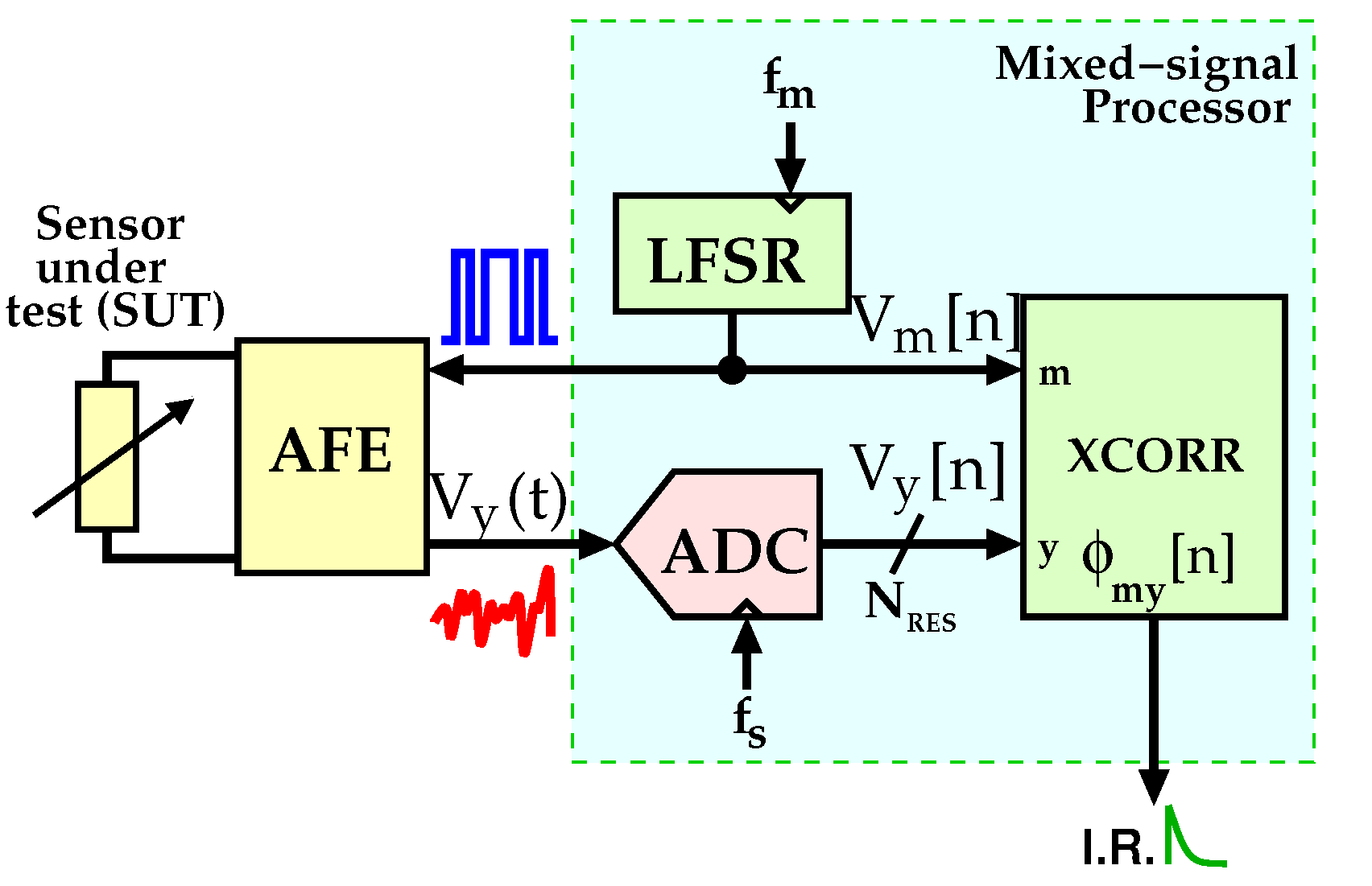
2.1. Overview and Conventional Approach

MLS-based signals are used as broadband excitation signals for sensors under test (SUT). These signals are a subclass of pseudo-random binary sequences (PRBS) and are generated through simple digital circuits called linear feedback shift registers (LFSR). Given L is the order of a generic LFSR, it generates an MLS of N = 2 L 1 binary symbols. LFSR circuits find countless applications in information theory, one of which is the measurement of the impulse response (IR) of linear and time-invariant (LTI) systems. Let m [ n ] be the MLS input of an LTI system, y [ n ] its output array, and h [ n ] its IR. The latter can be measured by cross-correlating the input array, m, with the output array, y, as follows [5,12]:
Φ m y [ n ] = m [ n ] 🟉 y [ n ] = 1 N j = 0 N 1 m [ i n ] · y [ i ] = Φ m m [ n ] h [ n ] h [ n ]
where the [ i n ] index is evaluated by modulo N, 🟉denotes the circular cross-correlation operation, Φ m m is the circular auto-correlation of the m sequence, and ∗ denotes the convolution operator. Since for high N values Φ m m [ n ] approximates the Kronecker delta function, δ [ n ] , the approximate result of the circular cross-correlation between Φ m m [ n ] and h [ n ] is actually h [ n ] .
This principle is implemented by the conventional architecture shown in Figure 1. The system consists of an LFSR that generates the V m [ n ] input signal for the AFE, which embeds the SUT. The clock signal of the LFSR has a frequency equal to f m . The AFE output, V y ( t ) , is sampled from the ADC with a sampling rate equal to f s . Thus, the digital cross-correlation operation is carried out, taking the V m [ n ] input and the V y [ n ] output as operators. Finally, the Φ m y system output is approximately equal to the IR of the composite system formed by the AFE and the sensor. The conventional architecture seen in Figure 1 exhibits a drawback concerning the error in the measured IR. This error comes from the electronic noise of the AFE and to a greater extent from the quantization noise of the ADC, which must have a high resolution in order to increase the signal-to-noise ratio (SNR) of the measured IR [5]. Moreover, the sampling rate of the ADC must be greater than or equal to the MLS frequency in order to convert enough samples for the cross-correlation operation.
As a novelty with respect to state-of-the-art features, the proposed circuit aims to increase the SNR of the measured IR by realizing the cross-correlation operation through an analog circuit. The analog-to-digital conversion is moved after the signal processing. This solution exhibits the following key advantages:
  • The quantization noise no longer affects the cross-correlation operation; thus, only the electronic noise contributes to the error in the measured IR;
  • Since the ADC must convert only the last sample of the entire cross-correlation process, the sampling rate requirement of the ADC is greatly relaxed;
  • RAM usage is totally avoided, simplifying the digital design of the system.

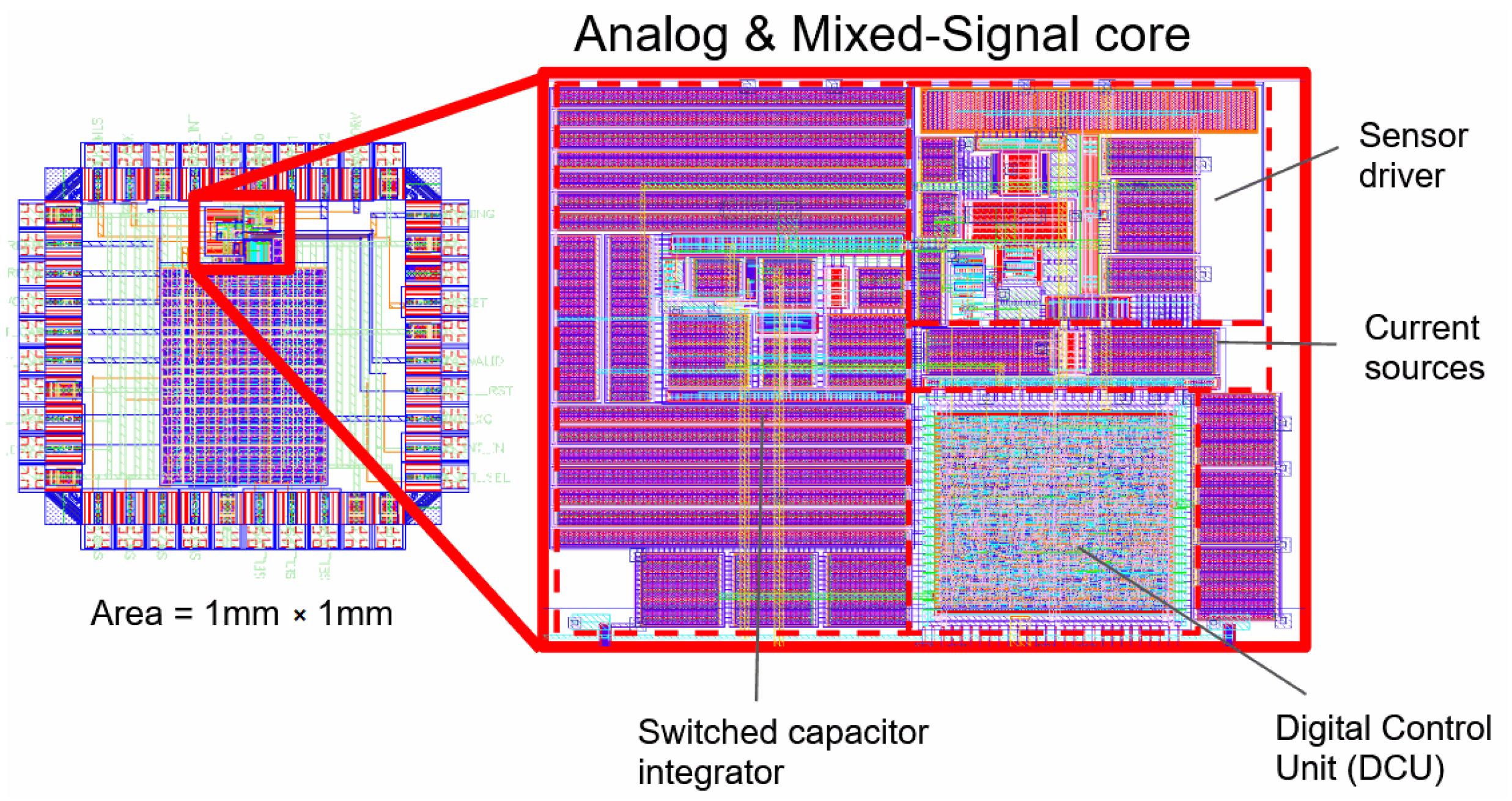
2.2. Proposed Analog Solution

The aforementioned principle of IR measurement is adopted here to measure the discrete-time inverse Laplace transform of a generic sensor’s impedance, henceforth referred to as Z s ( s ) . Figure 2 depicts the proposed analog solution. The system consists of three main blocks:
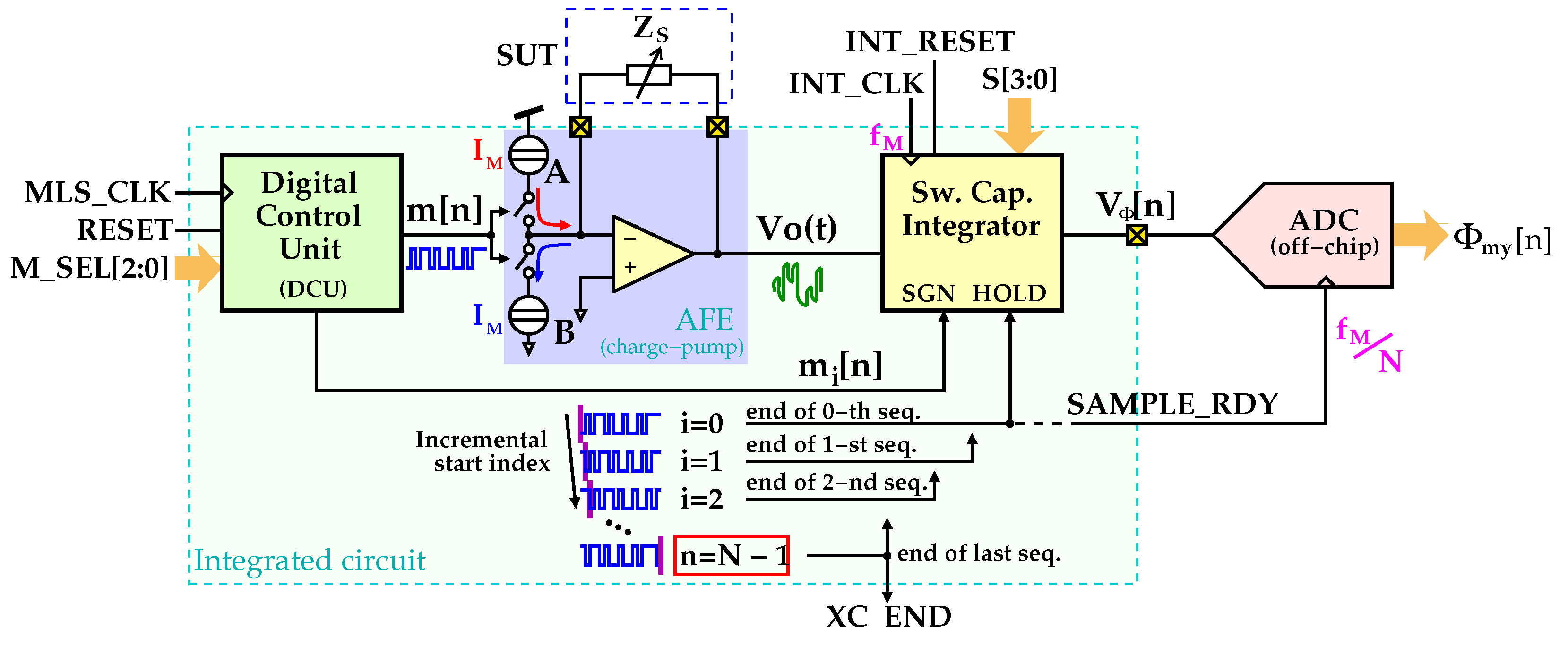
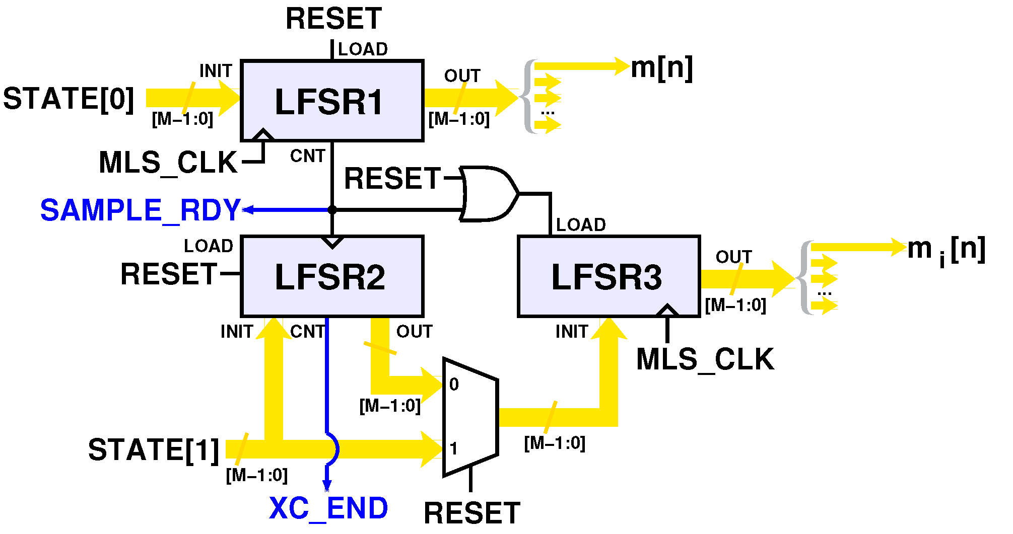
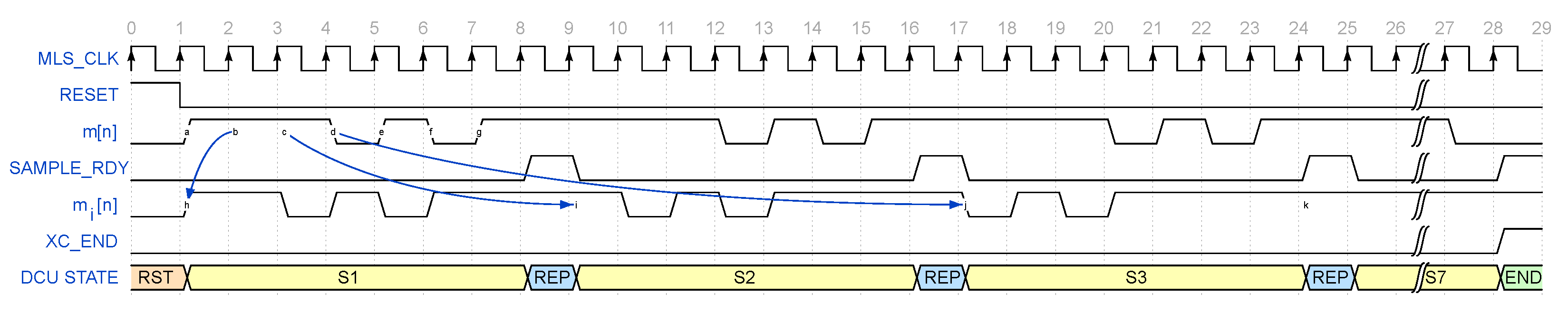
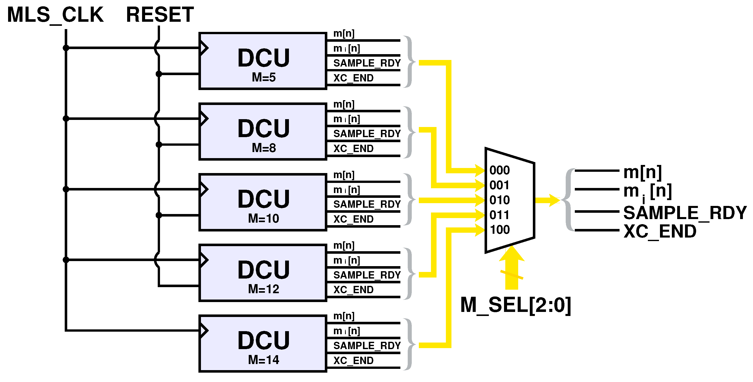
  • Digital Control Unit (DCU): This unit generates two MLS sequences, namely m and mi, expressed here as arrays. More specifically, m is a standard MLS, whereas mi replicates m with an i start index that is incremented at every completion of m. The clock frequency of the DCU is the same as that of the MLS, i.e., f m . The M number of binary symbols is selected by the user through the M_SEL configuration word. The DCU is also responsible for the generation of the SAMPLE_RDY and XC_END control signals;
  • AFE (analog front end): This is a charge pump-based front-end circuit for the SUT. It drives the sensor with a pseudo-random binary current signal of ± I m amplitude. This current signal is generated from the m sequence. The output of the AFE is the voltage across the sensor in response to the binary current;
  • Switched-Capacitor Integrator: This integrates the V o ( t ) voltage into the discrete time. Its clock signal is provided through the INT_CLK input port and it has the same clock frequency as the MLS, i.e., f m . The integrator has the option to change the gain of the integration through the S configuration word. Moreover, the sign of the integration can be changed through the SGN binary input. This feature is essential in order to properly implement the cross-correlation operation in an analog fashion. Regarding the HOLD input, when set to 1, the integrator stops its operation while maintaining the stored value. The integrator’s output voltage, V Φ [ n ] , is the output of the system and it is sampled by an external ADC at a lower sample rate as the SAMPLE_RDY signal goes higher.
As mentioned before, mi is a circularly shifted replica of m, with i being the start index that is incremented at every sequence completion. As the RESET signal (active high) returns to 0, the system starts its operation and the DCU starts generating the m and mi sequences. The MLS array is expressed as follows:
m = [ b 0 , b 1 , b 2 , , b N 1 ]
where the terms in m are binary symbols with values equal to ± 1 . The N × N MLS circulant matrix, formed by the shifted m sequences, is expressed as follows:
C = b 0 b 1 b N 2 b N 1 b 1 b 2 b N 1 b 0 b N 2 b N 1 b N 4 b N 3 b N 1 b 0 b N 3 b N 2 = m 0 m 1 m N 2 m N 1
With reference to Figure 2, the discrete-time V o [ n ] voltage sampled with a sampling period of T s = 1 / f m is expressed as follows:
V o [ n ] T S · L 1 { | I m | · Z s ( s ) } | t = n · T S
where the T S scaling factor comes from the discrete-to-continuous time conversion performed by the AFE circuit. The latter acts as a 1-bit digital-to-analog converter (DAC) followed by a sample and hold. This operation, which can be described by a zero-order hold (ZOH) mathematical model, is not a perfect digital-to-analog conversion [13] and this is the reason for the approximately equal sign in (4). The values of (4) are expressed as an N-sample array as follows:
V o = [ V o , 0 , V o , 1 , V o , 2 , , V o , N 1 ]
The discretized time-domain impedance, i.e., the inverse Laplace transform of the Z s ( s ) sensor’s impedance, is given by cross-correlating the V o [ n ] output voltage with m [ n ] . This is accomplished through the integrator, whose integration’s sign selection implements the multiplication between the analog voltage and the MLS sequence. Indeed, the latter only includes binary values equal to ± 1 . The integrator’s output voltage, V Φ [ n ] , has the following expression in the discrete-time domain:
V Φ [ n ] = Γ · i = 0 N 1 m [ i n ] · V o [ i ]
where Γ is the integrator’s gain. By substituting (4) in (6) and thanks to (1), the following equation is obtained:
V Φ [ n ] T S · Γ · N · | I m | · Φ m m [ n ] L 1 { Z s ( s ) } | t = n · T S
where Φ m m [ n ] is the circular auto-correlation of the m [ n ] sequence and ∗ denotes the convolution operator. The discrete-time impedance appears in (7) instead of the impulse response since the input and the output of the SUT are a current and a voltage, respectively. The VΦ array, comprising the sampled values of the integrator’s output, is defined as follows:
V Φ = [ V Φ , 0 , V Φ , 1 , V Φ , 2 , , V Φ , N 1 ]
The approximated expression of the discretized time-domain impedance of the sensor is obtained from the integrator’s voltage, V Φ [ n ] , as follows:
V Φ [ n ] ψ L 1 { Z s ( s ) } | t = n · T S
where ψ is a scaling factor and is equal to T S · Γ · N · | I m | . Equation (6) can be expressed in compact form using matrix multiplication. Thus, the C circulant matrix generated from the DCU and expressed in (3) is introduced:
V Φ = Γ · ( C V o )
Following the approach developed for (9), the same result in matrix form is obtained:
V Φ ψ = h z L 1 { Z s ( s ) } | t = 0 L 1 { Z s ( s ) } | t = T S L 1 { Z s ( s ) } | t = ( N 2 ) · T S L 1 { Z s ( s ) } | t = ( N 1 ) · T S
Besides the aforementioned advantages, the solution also exhibits a drawback concerning an increase in the measurement time. This is the amount of time needed to perform the entire cross-correlation operation and it can be derived as follows:
t m e a s = N · ( N + 1 ) f m
Comparing the t m e a s with that in the conventional approach of [5], it turns out that the measurement time required by the analog approach is N + 1 times greater than the conventional approach.

3. Circuit Design

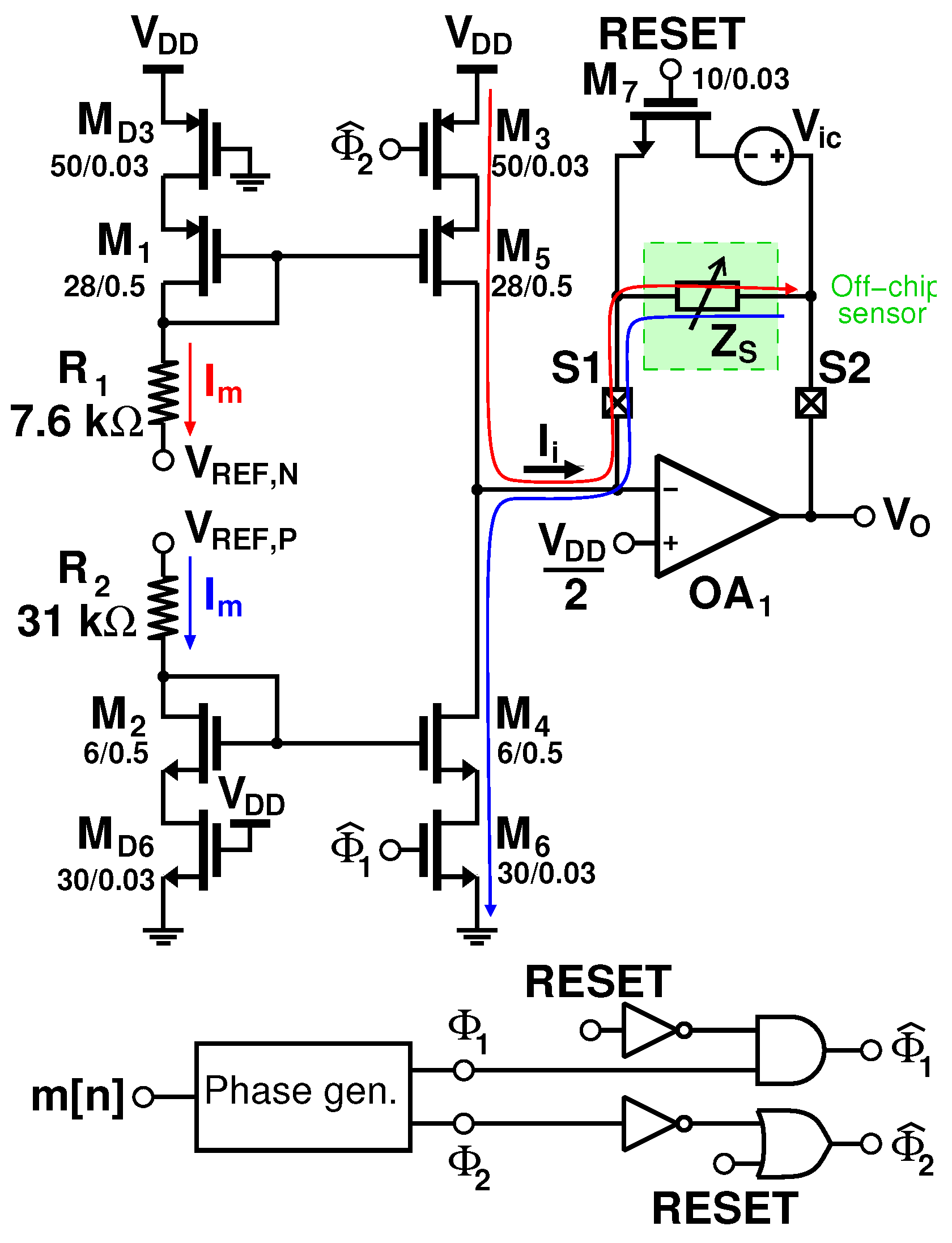
3.1. Analog Front End (AFE)

Figure 3 shows the circuit schematic of the AFE.
The circuit is based on a charge-pump architecture. The voltages V R E F , P and V R E F , N are provided by an external voltage source, which set them at 800 m V and 100 m V , respectively. These voltages were chosen to obtain the same current value, | I m | , equal to 10 μA for both branches. The currents are then mirrored by M 1 M 5 and M 2 M 4 current mirrors. M D 3 and M D 6 are dummy transistors and they are always in an on state with the aim of equalizing the drain-source voltages, V D S , of the M 3 and M 6 switches in order to increase the accuracy of the mirrored currents. The Z s sensor is connected between the pads S1 and S2. The gate terminals of the M3 and M6 switches are driven by Φ 1 ^ and Φ 2 ^ signals, which are generated by a non-overlapping phase generator starting from the m sequence. The M7 switch is driven by the RESET signal and it is turned on at every sequence completion. Its aim is to force the Z S terminals at a V D D / 2 + V i c voltage. V i c represents the sensor’s initial condition and it is pre-computed by a MATLAB simulation. Since an approximate value of V i c is used in the results in Section 4, an error in the cross-correlation operation is expected from the simulations.
As for the implementation of the OA1 opamp, a two-stage Miller architecture was adopted, as depicted in Figure 4. The simulated specifications of the frequency response in a typical corner are reported in Table 1.
The differential pair made up of the M 1 and M 2 MOSFETs was designed using low-threshold voltage (LVT) devices offered by the adopted FD-SOI technology. The sizing criterion for the opamp specifications in terms of the gain and GBW (henceforth called ω T ) is detailed as follows. By assuming a dominant pole model for the opamp having A 0 gain and ω B pole, the approximated transfer function from the I i ( s ) input current to the V o ( s ) output voltage of the AFE in Figure 3 can be derived as follows:
H z ( s ) = V o ( s ) I i ( s ) R s s · 1 ω S + 1 ω T + 1 = R s s · τ + Δ τ + 1
where ω T is the A 0 · ω B product, ω S = 1 / τ is the sensor’s pole equal to 1 / ( R S · C S ) , and Δ τ = 1 / ω T is the error in the measured sensor’s constant time due to the finite gain and bandwidth of the opamp. The relative error can be derived as follows:
ϵ τ = Δ τ τ = 1 R S · C S · ω T
The desired error depends on the application and the sensor. As an application example, the case of impedance spectroscopy of a metal-oxide (MOX) gas sensor could be considered for the ω T sizing. These sensors exhibit a typical parasitic capacitance, C S , of about 1 p F and a wide resistance value, R S , from a few kΩ to several MΩ [14]. For instance, assuming a typical resistance value of 160 kΩ, in order to achieve an error of 1% on the measured τ [5], it turns out from (14) that an opamp with a ω T greater than 100 M Hz is needed.

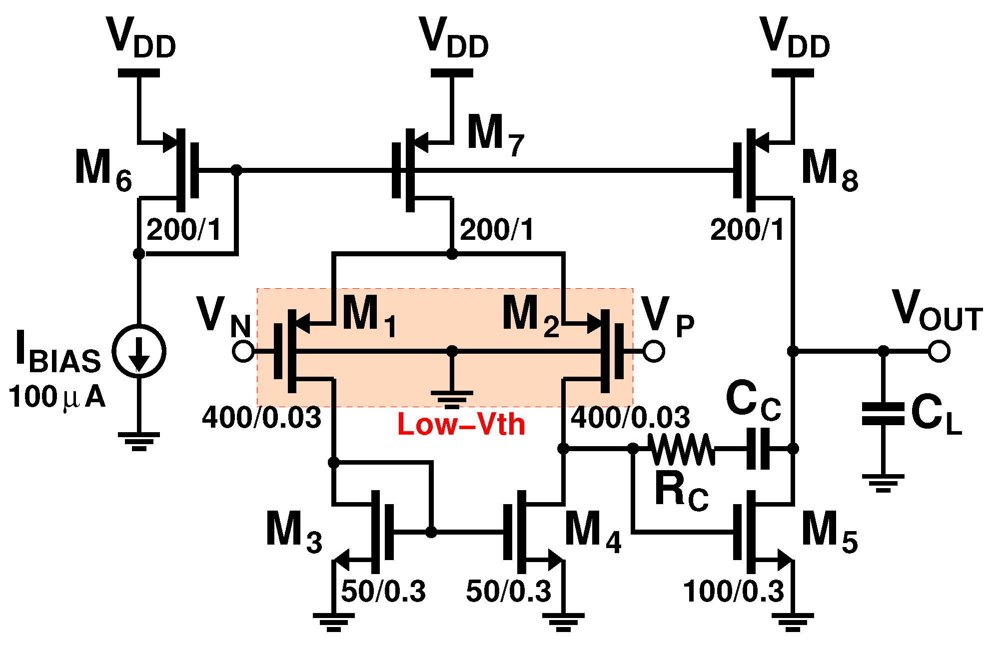
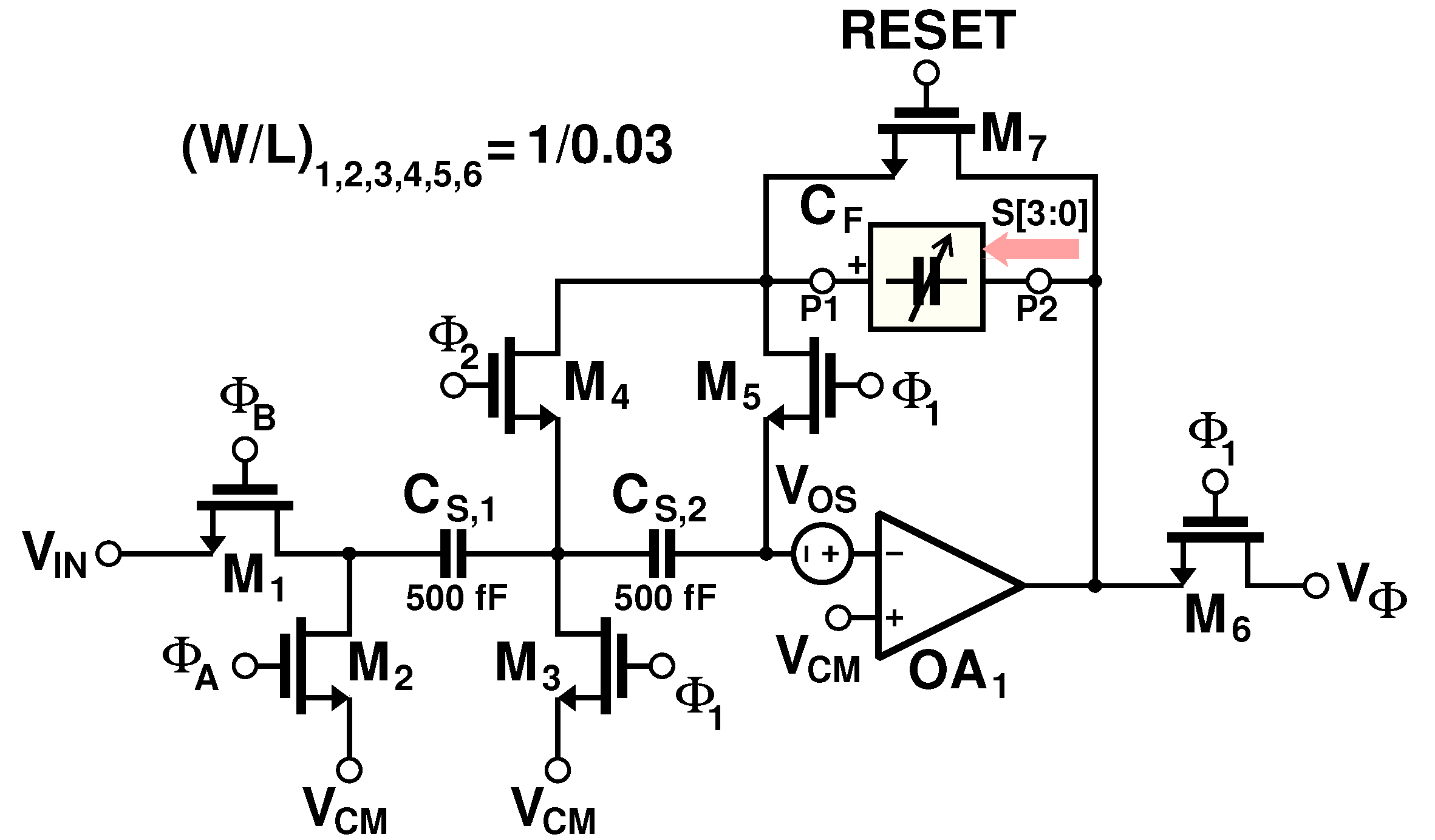
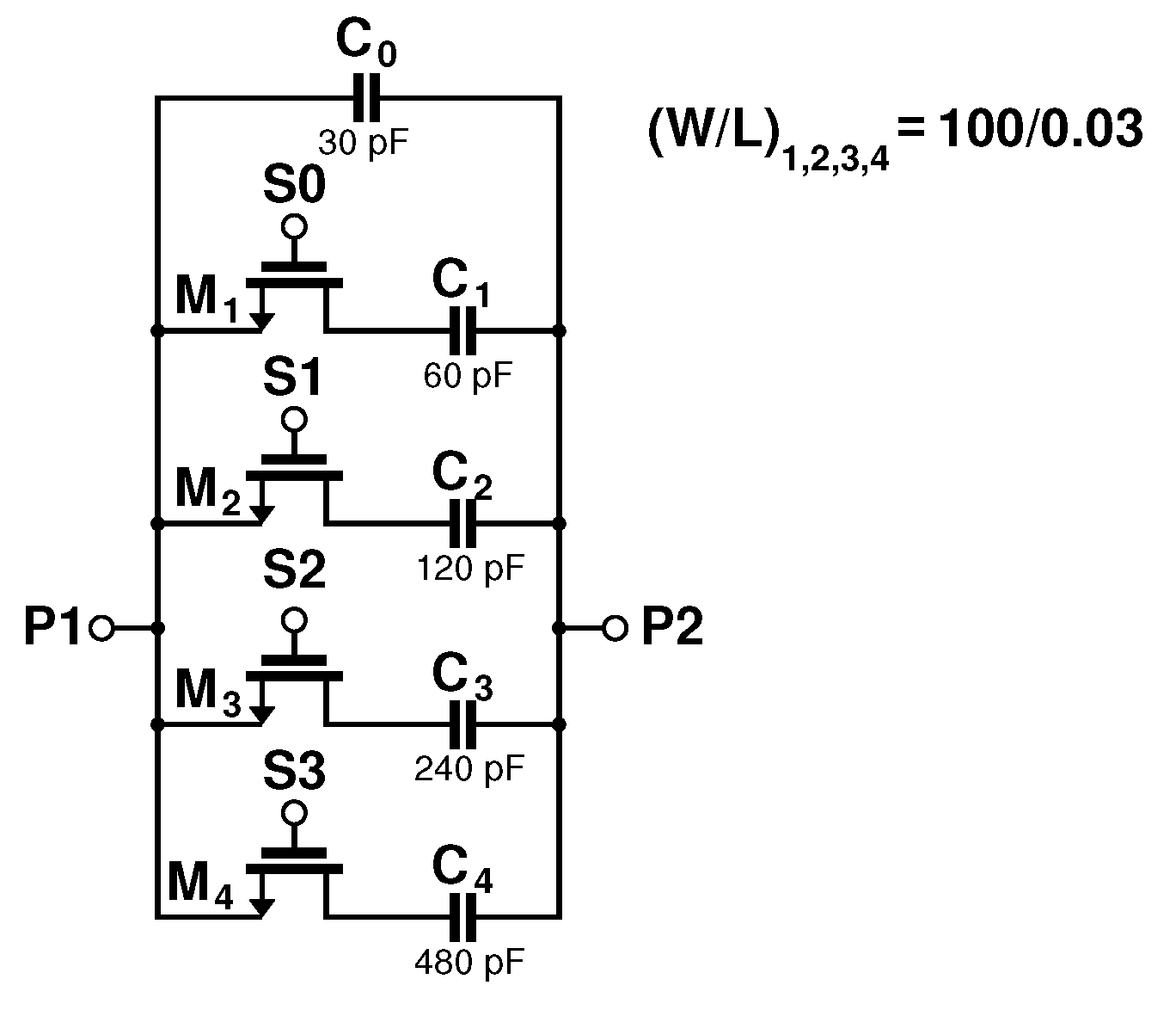
3.2. Switched-Capacitor Integrator

Figure 5 shows the adopted circuit schematic of the switched-capacitor integrator. The chosen architecture can be found in [15,16,17] and resembles the classical schematic of a stray insensitive integrator. The circuit employs the correlated double-sampling (CDS) technique in order to remove the effects of both the offset voltage and the flicker noise of the OA1 opamp. Similar to the sensor driver, the common-mode voltage, V c m , was set to V D D / 2 , which is 500 m V . The generator V O S in the schematic represents the offset contribution of the opamp. The C F feedback capacitor assumes discrete values according to the S configuration word. By changing this, the user changes the integration gain, Γ , depending on the application and the sensor’s dynamic behavior. The sign of the integration, which is useful for the accomplishment of the multiplication by the m binary samples, is changed by swapping the clock phases of the M1 and M2 MOSFETs. In particular, as Φ A coincides with Φ 1 and Φ B coincides with Φ 2 , the integration sign is negative. On the contrary, as Φ A coincides with Φ 2 and Φ B coincides with Φ 1 , the integration sign is positive. The C S , 2 auxiliary capacitor stores the V O S offset voltage and the input-referred flicker noise contributions of the opamp during the sampling operation (M1, M3, M4, M6 in an on state). These contributions are subtracted from the integrated value during the integration operation (M2, M5 in an on state). The same opamp as in Figure 4 was used for the OA1 implementation.
The phase-swapping operation is performed using the digital circuit depicted in Figure 6. The Φ A and Φ B signals are generated starting from the INT_CLK clock signal with a frequency equal to f m . With reference to the upper circuit in Figure 6, the INT_CLK clock and its inverted replica are swapped through two multiplexers. Thus, as the SGN signal assumes a high value, Φ A coincides with Φ 1 and Φ B coincides with Φ 2 . As the SGN assumes a low value, Φ A is equal to Φ 2 and Φ B is equal to Φ B .
The choice of the f m sampling frequency for the discrete-time integrator also limits the max detectable bandwidth of the system for the SUT to f m / 2 .

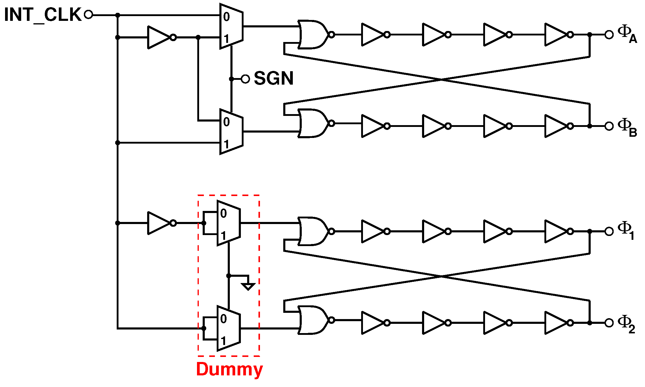
3.3. Digital Control Unit (DCU)

The core architecture of the DCU is depicted in Figure 7. The circuit includes three Galois LFSR registers [5], namely LFSR1, LFSR2, and LFSR3; an OR logic port; and a multiplexer. These registers have the option to load a start state through the INIT input buses. The loading is triggered by the LOAD input signal (active high). Additionally, they have an internal logic that is able to set the CNT output signal to 1 as the MLS is completed. The LOAD inputs of both LFSR1 and LFSR2 are connected to the global RESET of the DCU. The CNT output of LFSR1, SAMPLE_RDY, is used as a clock signal for LFSR2. STATE [ 0 ] and STATE [ 1 ] are pre-computed digital words and are the first and second states, respectively, of the LFSRs. The circuit’s operation is explained with reference to the simplified case of a 3-bit (N equal to 7) LFSR seen in Figure 8.
As the global RESET signal is asserted (0th cycle), LFSR1 and LFSR2 load the STATE [ 0 ] and STATE [ 1 ] words, respectively. LFSR3 loads the STATE [ 1 ] word since its LOAD input, i.e., the output of the OR port is set to 1 and the “1” input of the multiplexer is selected. During the first complete sequence (S1 state from the first to the seventh cycles), LFSR1 and LFSR3 produce exactly the same MLS sequence but the starting index of LFSR3 is incremented by 1 with respect to LFSR1. As LFSR1 and LFSR3 end their sequences (eighth cycle), their CNT outputs go high for a clock cycle (see SAMPLE_RDY at the eighth cycle). This output signals the end of the current sequence. During this clock cycle, the states of m and mi are repeated. Since the SAMPLE_RDY output serves as the clock input for LFSR2 at its positive edge, the state of LFSR2 accomplishes a step forward and becomes S2. Since the “0” input of the multiplexer is selected (the RESET signal is 0) and since the LOAD input of LFSR3 is 1, the LFSR3 initial state for the new sequence is incremented to S2. As a result, the starting index of the mi sequence will be incremented at every m completion (see the 9th and 17th cycles). The algorithm ends after seven repetitions during which the whole 7 × 7 C circulant matrix has been serially provided at the mi output. The end of the operation is signaled through the CNT output of LFSR2 (see XC_END at the 29th cycle).
A conventional way to accomplish the C matrix in integrated digital circuits is actually to hard-code the matrix content in a circuit made of tie cells. This solution works for very small matrices but fails as the required size increases. A more efficient solution is the adoption of a dedicated ROM memory but it could have a big area for large matrices. Moreover, the ROM size increases, as multiple C matrices of different M orders are required.
Multiple DCUs, each of a different LFSR order, M, were designed. As depicted in Figure 9, the implemented bit orders are 5 bit (only for test purposes), 8 bit, 10 bit, 12 bit, and 14 bit. Depending on the application, the user can choose the desired M order through the M_SEL signals.

3.4. Noise Estimation

Electronic noise plays a role in degrading the accuracy of the h z samples resulting from the analog cross-correlation operation. Only the thermal noise is considered since the effect of the flicker noise is assumed to be removed thanks to the implemented CDS technique implemented in the integrator [15,16,17]. The analytical expression of the integrated thermal noise at the system’s output, V Φ n , can be derived by considering two main contributions: the noise from the AFE and the noise from the integrator. The first is calculated with reference to Figure 3 as follows:
v n o , A F E ¯ 2 γ · k T C S · R S · g m 4 , 5
where γ is the noise factor considered to be equal to 2/3, R S and C S are the electrical parameters of the sensor’s simplified model, and g m 4 , 5 is the small-signal transconductance of both the M4 and M5 MOSFETs in Figure 3. The latter was found to be very similar for both the M4 and M5 MOSFETs and it was determined through SPECTRE simulation to be about 200 μS. Regarding the contribution from the CDS integrator, an approximate expression for its input-referred noise can be found in [16]:
v n o , I N T ¯ 2 4 k T O S R · C S · 2
where C S is the sampling capacitor and the OSR is the oversampling ratio, whose value is, in this case, equal to the ratio between the integrator’s sampling frequency, f m , and the sampling frequency of the external ADC, which is f m / N . The approximate expression of the output-referred noise of the entire system, V Φ n , is derived as follows:
v Φ n ¯ 2 k T · C S C F 2 · 8 N · C S + γ · R s e n s · g m 4 , 5 C s e n s
Equation (17) proved to be useful for a first-order evaluation of the accuracy of the entire system.

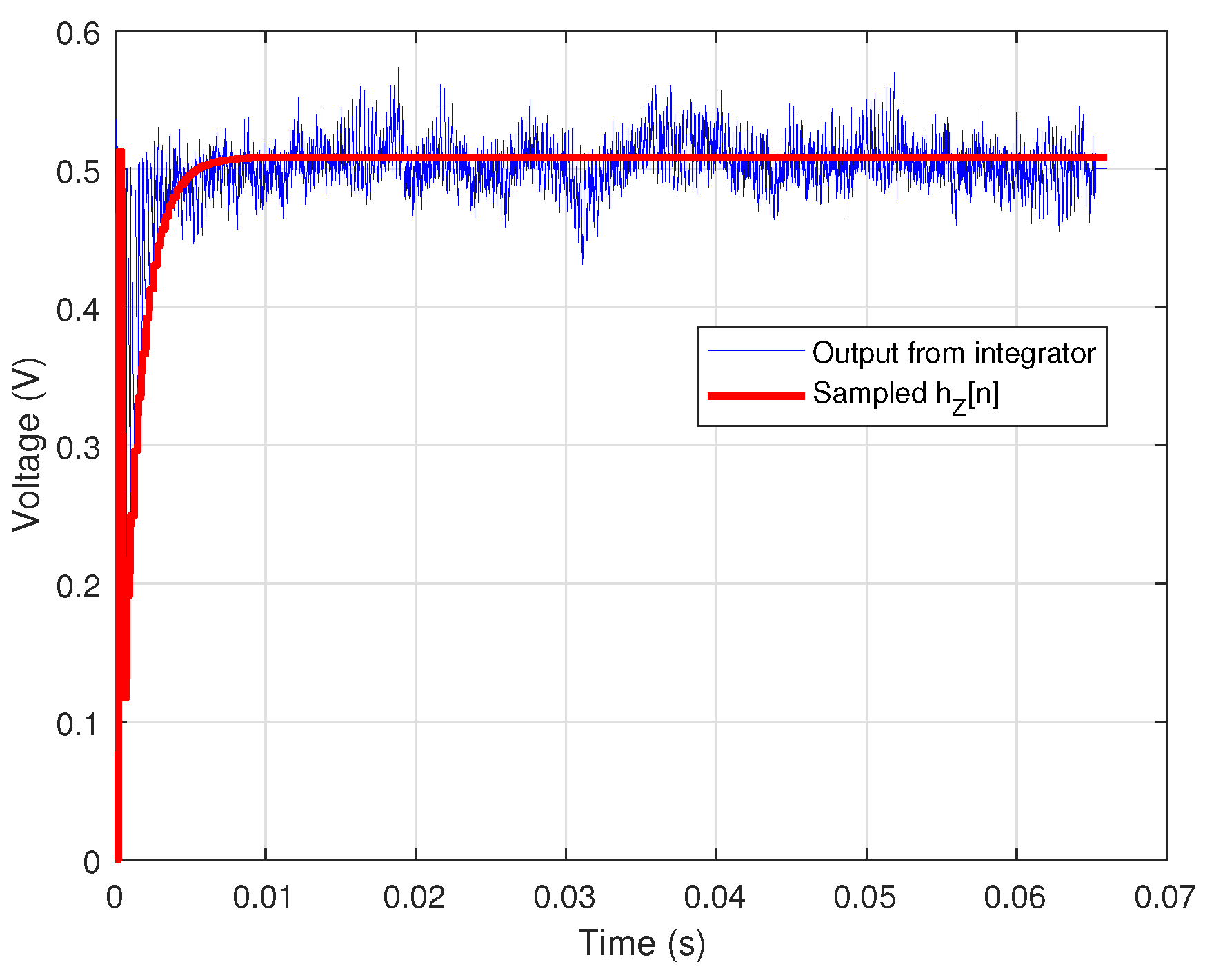
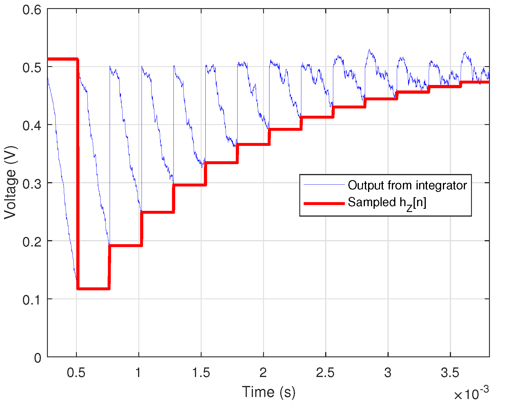
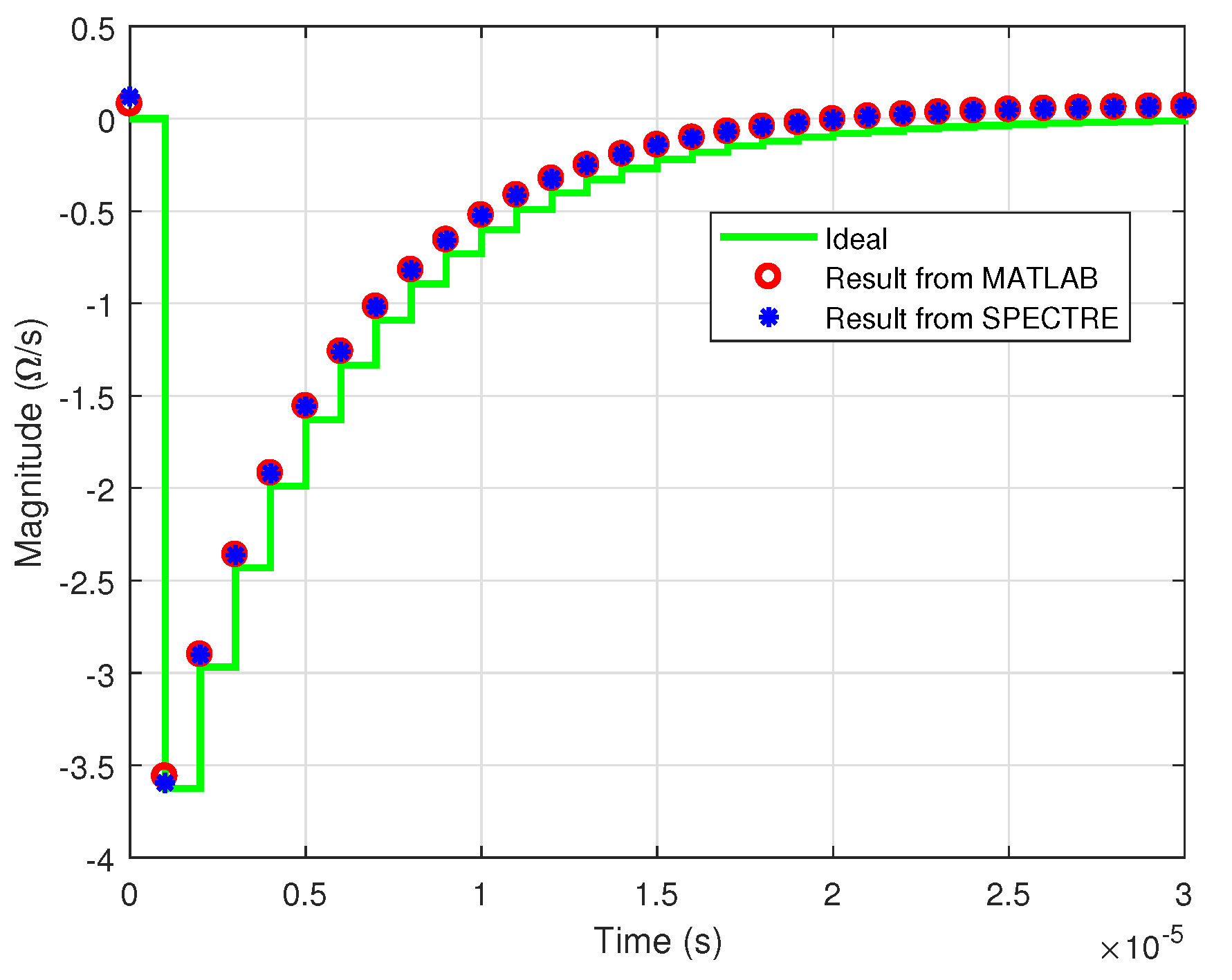
4. Simulation Results

The single blocks shown in Figure 2 were simulated and verified in the Cadence Virtuoso Platform through a SPECTRE simulation. However, the long time required for a complete cross-correlation simulation did not permit a transistor-level verification of the entire system. Thus, the AFE and integrator were modeled using transistor-level specifications with the Verilog-A models. In this way, it was possible to verify the correctness of the circuit’s operation.
Figure 10 depicts the waveforms from the simulation. In particular, a simple parallel RC circuit was used as the test impedance with an 8-bit MLS input signal and a sampling frequency, f m , of 1 M Hz . The latter limited the maximum detectable bandwidth to 500 k Hz . The sensor’s electrical components were chosen as 50 kΩ and 100 p F for the resistance and capacitance, respectively. The MLS current amplitude, | I m | , was set to 10 μA, as mentioned in Section 3.1. Regarding the integrator, the 30 p F value was selected from the variable capacitor seen in Figure 11 (S0, S1, S2, S3 inputs with low values), leading to an integration gain of 0.0167. The output voltage from the SPECTRE simulation was compared with that from the ideal MATLAB model in Figure 12.
Figure 13 shows the discrete-time analog cross-correlation from the SPECTRE simulation. As can be seen, the integrator’s output voltage (blue curve) was sampled by the external ADC to generate the cross-correlation samples (red curve). A detail of the cross-correlation operation is depicted in Figure 14. As derived in Section 2, the discretized time-domain impedance of the sensor, h z [ n ] , was obtained by multiplying the sampled version of the integrator’s output voltage (red curve in Figure 13) by the ψ scaling factor introduced in (9).
In Figure 15, the theoretical h z curve (green) is compared with the simulated results obtained from the MATLAB (red points) and SPECTRE (blue points) implementations, showing good agreement between them.
The thermal noise effect which, as also mentioned, impacts the system’s accuracy, was modeled in the simulation environment. Its effect can be observed in Figure 16, in particular, in the right portion of the curve. The criterion introduced in [5] was used here for the direct extraction of the SNR from the simulated output curve. Briefly, the time-based impedance was divided into two portions using the crossing of the curve on the X axis, i.e., the zero crossing point, as the discriminant index. In the left portion, the signal contribution was prevalent with respect to the noise, whereas in the right portion, the noise contribution was prevalent with respect to the signal. Thus, the signal power, P S , was computed through the following equation:
P S = 1 N · n = 0 i V Φ [ n ] ψ 2
where i is the zero-crossing index. Regarding the noise power, P N , it was computed by calculating the variance of the right portion by assuming a Gaussian distribution of the noise sources. As a result, a simulated SNR of 75 dB was obtained for the specific modeled sensor.
This value differed from the theoretical value obtained by considering only the thermal noise power derived in (17) in the SNR calculation. By substituting the values in the equation, a theoretical SNR of 100 dB was obtained. The discrepancy between the simulated and theoretical SNR can be explained by considering that the latter only took into account the thermal noise from the circuit, whereas the former also contemplated the precision error of the sensor’s initial condition. Indeed, the error voltage in the V i c voltage (see Figure 3) translated to a cross-correlation error which, in turn, impacted as an error in the discrete-time impedance of the sensor. Regarding the power consumption, a value of 420 μW was obtained from the simulation. In (12), the measurement time was equal to 65 m s for the considered test impedance and the used MLS frequency of 1 M Hz . The energy-per-measurement (EpM) value was obtained by multiplying the power consumption by the measurement time, resulting in 27.4 μJ for the simulated circuit.
Figure 17 shows the layout of the chip with an emphasis on the analog and mixed-signal core. The latter measures about 0.034   m m 2 .
Table 2 shows a performance comparison with state-of-the-art integrated systems for EIS. The max detected error of the presented work is comparable with [10]. However, it can be noted that although in [10] the error is taken from the absolute maximum INL over the measured frequency range, in the proposed work, it is obtained from the SNR of the entire simulated curve. In particular, the SNR is converted to an RMS error by considering the measurement error as a Gaussian noise signal referred to as a 1 V RMS amplitude sinusoidal signal. Thus, the specified error takes into account the error of the entire curve. The obtained RMS error is 0.0177%, which corresponds to 177 ppm. Although the error is comparable with those of state-of-the-art systems, the proposed solution exhibits the best performance in terms of power consumption per measured points. The number of measurable points can be increased up to 2 14 1 .

5. Conclusions

In this paper, an integrated circuit for the time-based measurement of sensors’ impedance has been presented. The circuit exploits the impulse response measurement concept through the use of maximum-length sequences and a cross-correlation operation. Unlike the conventional approach, the proposed solution implements the cross-correlation in the analog domain. This allows the analog-to-digital conversion to be moved after the signal processing, leading to several benefits: (1) the measured time-based impedance is not affected by the ADC’s quantization noise, thus increasing measurement accuracy; (2) the sampling rate of the ADC is greatly relaxed since only the last cross-correlation sample is converted, thus reducing the system’s complexity; and (3) RAM usage is avoided, thus reducing efforts in digital design. Theoretical concepts about the circuit’s design and operation were presented with consideration of the thermal noise phenomenon. The simulated performances were shown by testing a sensor’s equivalent model composed of a 50 kΩ resistor in parallel with a 100 p F capacitor. A time-based output impedance of 255 points was obtained with a maximum tested frequency of 500 k Hz and a simulated RMS error of 0.0177% (or 177 ppm).

Author Contributions

Conceptualization, A.V.R. and S.D.; methodology, A.V.R., S.C., L.F. and S.D.; software, A.V.R. and S.D.; validation, A.V.R. and S.D.; formal analysis, A.V.R. and S.D.; investigation, A.V.R. and S.D.; resources, S.D.; data curation, A.V.R.; writing—original draft preparation, A.V.R.; writing—review and editing, A.V.R. and S.D.; visualization, A.V.R.; supervision, S.D.; project administration, L.F. and S.D.; funding acquisition, L.F. and P.A.S. All authors have read and agreed to the published version of the manuscript.

Funding

This research was supported by the Apulia Region, Italy, through the SMEA PON Project, CUP: B84G14000070005.

Conflicts of Interest

The authors declare no conflict of interest.

Abbreviations

The following abbreviations are used in this manuscript:
ADCanalog-to-digital converter
AFEanalog front end
CMOScomplementary metal-oxide semiconductor
DCUdigital control unit
EISelectrical impedance spectroscopy
EpMenergy per measurement
FD-SOIfully depleted silicon on insulator
GBWgain-bandwidth product
IRimpulse response
LFSRlinear feedback shift register
LTIlinear time-invariant
MLSmaximum-length sequence
MOSFETmetal-oxide-semiconductor field-effect transistor
MOXmetal oxide
PMphase margin
PRBSpseudo-random binary sequence
RAMrandom access memory
SNRsignal-to-noise ratio
SUTsensor under test

References

  1. Bianchi, D.; Ferrari, G.; Rottigni, A.; Sampietro, M. CMOS Impedance Analyzer for Nanosamples Investigation Operating up to 150 MHz with Sub-aF Resolution. IEEE J. Solid-State Circuits 2014, 49, 2748–2757. [Google Scholar] [CrossRef]
  2. Xu, J.; Hong, Z. Low Power Bio-Impedance Sensor Interfaces: Review and Electronics Design Methodology. IEEE Rev. Biomed. Eng. 2022, 15, 23–35. [Google Scholar] [CrossRef]
  3. Beohar, N.; Malladi, V.N.K.; Mandal, D.; Ozev, S.; Bakkaloglu, B. Online Built-In Self-Test of High Switching Frequency DC–DC Converters Using Model Reference Based System Identification Techniques. IEEE Trans. Circuits Syst. Regul. Pap. 2018, 65, 818–831. [Google Scholar] [CrossRef]
  4. Islam, S.M.R.; Park, S.Y. Precise Online Electrochemical Impedance Spectroscopy Strategies for Li-Ion Batteries. IEEE Trans. Ind. Appl. 2020, 56, 1661–1669. [Google Scholar] [CrossRef]
  5. Radogna, A.V.; Capone, S.; Francioso, L.; Siciliano, P.A.; D’Amico, S. Performance Analysis of an MLS-Based Interface for Impulse Response Estimation of Resistive and Capacitive Sensors. IEEE Trans. Circuits Syst. Regul. Pap. 2022, 69, 3666–3678. [Google Scholar] [CrossRef]
  6. Kassanos, P.; Triantis, I.F.; Demosthenous, A. A CMOS Magnitude/Phase Measurement Chip for Impedance Spectroscopy. IEEE Sens. J. 2013, 13, 2229–2236. [Google Scholar] [CrossRef]
  7. Shumba, A.T.; Montanaro, T.; Sergi, I.; Fachechi, L.; De Vittorio, M.; Patrono, L. Leveraging IoT-Aware Technologies and AI Techniques for Real-Time Critical Healthcare Applications. Sensors 2022, 22, 7675. [Google Scholar] [CrossRef] [PubMed]
  8. Ferrari, G.; Bianchi, D.; Rottigni, A.; Sampietro, M. 17.4 CMOS impedance analyzer for nanosamples investigation operating up to 150 MHz with Sub-aF resolution. In Proceedings of the 2014 IEEE International Solid-State Circuits Conference Digest of Technical Papers (ISSCC), San Francisco, CA, USA, 9–13 February 2014; pp. 292–293. [Google Scholar] [CrossRef]
  9. Cheon, S.I.; Kweon, S.J.; Kim, Y.; Koo, J.; Ha, S.; Je, M. An Impedance Readout IC with Ratio-Based Measurement Techniques for Electrical Impedance Spectroscopy. Sensors 2022, 22, 1563. [Google Scholar] [CrossRef]
  10. Crescentini, M.; Bennati, M.; Tartagni, M. A High Resolution Interface for Kelvin Impedance Sensing. IEEE J. Solid-State Circuits 2014, 49, 2199–2212. [Google Scholar] [CrossRef]
  11. Luciani, G.; Crescentini, M.; Romani, A.; Chiani, M.; Benini, L.; Tartagni, M. Energy-Efficient PRBS Impedance Spectroscopy on a Digital Versatile Platform. IEEE Trans. Instrum. Meas. 2021, 70, 6501912. [Google Scholar] [CrossRef]
  12. Radogna, A.V.; D’Amico, S.; Capone, S.; Francioso, L. A Simulation Study of an Optimized Impedance Spectroscopy Approach for Gas Sensors. In Proceedings of the 2019 IEEE 8th International Workshop on Advances in Sensors and Interfaces (IWASI), Otranto, Italy, 13–14 June 2019; pp. 142–147. [Google Scholar] [CrossRef]
  13. Rife, D.D.; Vanderkooy, J. Transfer-Function Measurement with Maximum-Length Sequences. J. Audio Eng. Soc. 1989, 37, 419–444. [Google Scholar]
  14. Radogna, A.V.; Capone, S.; Francioso, L.; Siciliano, P.A.; D’Amico, S. A 296 nJ Energy-per-Measurement Relaxation Oscillator-Based Analog Front-End for Chemiresistive Sensors. IEEE Trans. Circuits Syst. Regul. Pap. 2021, 68, 1123–1133. [Google Scholar] [CrossRef]
  15. Nagaraj, K.; Vlach, J.; Viswanathan, T.; Singhal, K. Switched-capacitor integrator with reduced sensitivity to amplifier gain. Electron. Lett. 1986, 22, 1103. [Google Scholar] [CrossRef]
  16. Im, S.; Park, S.G. A 154-μW 80-dB SNDR analog-to-digital front-end for digital hearing aids. Analog Integr. Circuits Signal Process. 2016, 89, 383–393. [Google Scholar] [CrossRef]
  17. Boni, A.; Giuffredi, L.; Pietrini, G.; Ronchi, M.; Caselli, M. A Low-Power Sigma-Delta Modulator for Healthcare and Medical Diagnostic Applications. IEEE Trans. Circuits Syst. Regul. Pap. 2022, 69, 207–219. [Google Scholar] [CrossRef]
  18. Xu, J.; Harpe, P.; Van Hoof, C. An Energy-Efficient and Reconfigurable Sensor IC for Bio-Impedance Spectroscopy and ECG Recording. IEEE J. Emerg. Sel. Top. Circuits Syst. 2018, 8, 616–626. [Google Scholar] [CrossRef] [Green Version]
Figure 1. Conventional architecture for MLS-based EIS of sensors.
Electronics 11 03807 g001
Figure 2. System architecture of the proposed integrated analog and mixed-signal solution.
Electronics 11 03807 g002
Figure 3. Circuit schematic of the implemented AFE. The specified width/length are reported in μm for each MOSFET.
Electronics 11 03807 g003
Figure 4. Circuit schematic of the implemented opamp for the sensor driver. The specified width/length are reported in μm for each MOSFET.
Electronics 11 03807 g004
Figure 5. Circuit schematic of the implemented switched-capacitor integrator. The specified width/length are reported in μm for each MOSFET.
Electronics 11 03807 g005
Figure 6. Circuit schematic of the non-overlapping phase generator (bottom) and the phase-swapping generator (top) for the switched-capacitor integrator.
Electronics 11 03807 g006
Figure 7. Circuit schematic of the digital control unit (DCU) for the generation of MLS sequences.
Electronics 11 03807 g007
Figure 8. Waveform diagram of the DCU signals by considering an L equal to 3 (N equal to 7).
Electronics 11 03807 g008
Figure 9. Circuit schematic of the implemented selectable DCU.
Electronics 11 03807 g009
Figure 10. Waveforms from SPECTRE simulation.
Electronics 11 03807 g010
Figure 11. Circuit schematic of the variable capacitor C F . The specified width/length are reported in μm for each MOSFET.
Electronics 11 03807 g011
Figure 12. Comparison of AFE output voltages from theoretical (MATLAB) and circuit-level (SPECTRE) simulations.
Electronics 11 03807 g012
Figure 13. Integrator’s output voltage (blue curve) and its sampled replica (red curve).
Electronics 11 03807 g013
Figure 14. Detail of the cross-correlation operation.
Electronics 11 03807 g014
Figure 15. Theoretical time-based EIS (green curve) compared with simulation results from MATLAB (red points) and SPECTRE (blue points) implementations, respectively.
Electronics 11 03807 g015
Figure 16. Ideal output from MATLAB implementation (blue curve) compared with output from SPECTRE (red points) in presence of thermal noise.
Electronics 11 03807 g016
Figure 17. Chip layout.
Electronics 11 03807 g017
Table 1. Specifications of the designed opamp obtained through circuit simulations.
ParameterValue
DC Gain60 dB
Gain-Bandwidth Product (GBW)105 M Hz
Phase Margin (PM)53 Deg
Table 2. Comparison with state-of-the-art systems.
[10][9][6][18]This Work
ApproachFrequency-based
(ΔΣ demodulation)
Frequency-based
(magnitude/real part
measurement)
Frequency-based
(magnitude/phase
measurement)
Frequency-based
(MLS/DMLS + read-out, 
DSP not included)
Time-based
(MLS + analog
cross-correlation)
CMOS Process0.35 μm180 nm0.35 μm180 nm28 nm FD-SOI
Chip area9 mm2N/A0.4 mm2N/A0.034 mm2 (core)
Tested impedance    68 Ω ‖ 1 μF200 Ω +
(5 kΩ ‖ 45 nF)
Equivalent circuit of the
electrode/tissue impedance
100 Ω ‖
(100 Ω + 220 nF)
50 kΩ ‖ 100 pF
Stimulus
generator
YesNoNoYesYes
Max tested
frequency
16 kHz1 MHz100 kHz125 kHz500 kHz (capable of
measuring up to 50 MHz)
Measured points11163255 (capable of measuring        
up to 2 14 points)
Max Error0.0166 % (INL)0.3% (magnitude
error, simulated)
1.15% (magnitude error)>10% (resistor error)0.0177% (RMS on entire
curve, simulated)
Max power
consumption
5.8 mW0.513 mW21 mW0.155 mW0.420 mW
Publisher’s Note: MDPI stays neutral with regard to jurisdictional claims in published maps and institutional affiliations.

