Article

A Cost-Effective and Compact All-Digital Dual-Loop Jitter Attenuator for Built-Off-Test Applications

Department of Electronic and Electrical Engineering, Hongik University, Seoul 06983, Korea
*
Author to whom correspondence should be addressed.
Electronics 2022, 11(21), 3630; https://doi.org/10.3390/electronics11213630
Submission received: 20 October 2022 / Revised: 2 November 2022 / Accepted: 4 November 2022 / Published: 7 November 2022
(This article belongs to the Special Issue Mixed Signal Circuit Design)

Abstract

:
A compact and low-power all-digital CMOS dual-loop jitter attenuator (DJA) for low-cost built-off-test (BOT) applications such as parallel multi-DUT testing is presented. The proposed DJA adopts a new digital phase interpolator (PI)-based clock recovery (CR) loop with an adaptive decimation filter (ADF) function to remove the jitter and phase noise of the input clock, and generate a phase-aligned clean output clock. In addition, by adopting an all-digital multi-phase multiplying delay-locked loop (MDLL), eight low-jitter evenly spaced reference clocks that are required for the PI are generated. In the proposed DJA, both the MDLL and PI-based CR are first-order systems, and so this DJA has the advantage of high system stability. In addition, the proposed DJA has the benefit of a wide operating frequency range, unlike general PLL-based jitter attenuators that have a narrow frequency range and a jitter peaking problem. Implemented in a 40 nm 0.9 V CMOS process, the proposed DJA generates cleaned programmable output clock frequencies from 2.4 to 4.7 GHz. Furthermore, it achieves a peak-to-peak and RMS jitter attenuation of –25.6 dB and –32.6 dB, respectively, at 2.4 GHz. In addition, it occupies an active area of only 0.0257 mm2 and consumes a power of 7.41 mW at 2.4 GHz.

1. Introduction

With the continuous development of semiconductor scaling technology, the I/O interface operation speed of high-speed DRAMs such as DDR5 (=7.2 Gbps/pin), LPDDR5 (=6.4 Gbps/pin), and GDDR6 (=16 Gbps/pin) has also dramatically increased. Accordingly, the complexity and importance of memory device testing required for performance evaluation and the defect detection of high-speed DRAM and NAND flash memory ICs are increasing. In addition, the test cost accounts for a significant portion of the overall manufacturing cost of high-speed ICs. An essential factor in this increase in test cost is the increase in the price of automatic test equipment (ATE) used to test high-speed memory ICs. In particular, for the at application speed (at-speed) test of the latest high-speed DRAMs, ATE has often needed to be replaced with a faster and more expensive version to support the ever-increasing device-under-test (DUT) speed. This is because it is challenging to maintain the signal integrity characteristics of a multi-channel ATE, which requires the parallel testing (or multisite testing) [1,2] of multiple DUTs using multiple high-speed I/O channels at the same time. In addition, when evaluating the performance of high-speed DUTs, the limited clock frequency and significant clock jitter (or phase noise) characteristics of the existing low-cost ATEs supporting parallel multi-DUT testing may decrease the test accuracy.
Recently, it has been proposed to use a built-off-test (BOT) or built-off-self-test (BOST) module as a cost-effective method for the at-speed testing of high-speed memory ICs [3,4,5]. As shown in Figure 1, the BOT (or BOST) module is used as a bridge connecting the DUT and the ATE. One of the key technologies in implementing such a parallel multi-DUT test system is a PLL-based clock generator that removes the jitter of the noisy reference clock provided by the low-cost ATE and multiplies the clock frequency. A common way to perform jitter cleaning and frequency multiplication simultaneously is to use two PLLs connected in series [6,7]. For example, as shown in Figure 1, the first PLL #1 cleans the reference clock jitter, and the second PLL #2 generates a multiplied output clock. As shown in Figure 2a, the conventional PLL #1, which operates as a jitter attenuator (or jitter cleaner), uses an external voltage-controlled crystal oscillator (VCXO) and external loop filters to lower the loop bandwidth, leading to a severe increase in area and power consumption. Since a general PLL-based jitter attenuator has a limited operating frequency range, to make a jitter attenuator supporting a wide frequency range, there is a method using a plurality of PLLs and RF switches, as shown in Figure 2b [8]. However, with this method it is challenging to apply to the BOT-based parallel multi-DUT test system because the size, power consumption, and cost of the jitter attenuator are increased too severely.
This paper presents a small form factor, low-power CMOS jitter attenuator for a low-cost BOT-based parallel multi-DUT test system. The proposed all-digital dual-loop jitter attenuator (DJA) utilizes a low-jitter multiplying delay-locked loop and a new phase interpolator-based clock recovery loop to operate in the wide frequency range of 2.4~4.7 GHz. The proposed DJA can remove the jitter and phase noise of the input clock and generate an output clock aligned with the average frequency of the input clock. The rest of this paper is organized as follows. Section 2 presents the architecture and operation of the proposed dual-loop jitter attenuator. Section 3 describes the experimental results. Finally, Section 4 presents the conclusion.

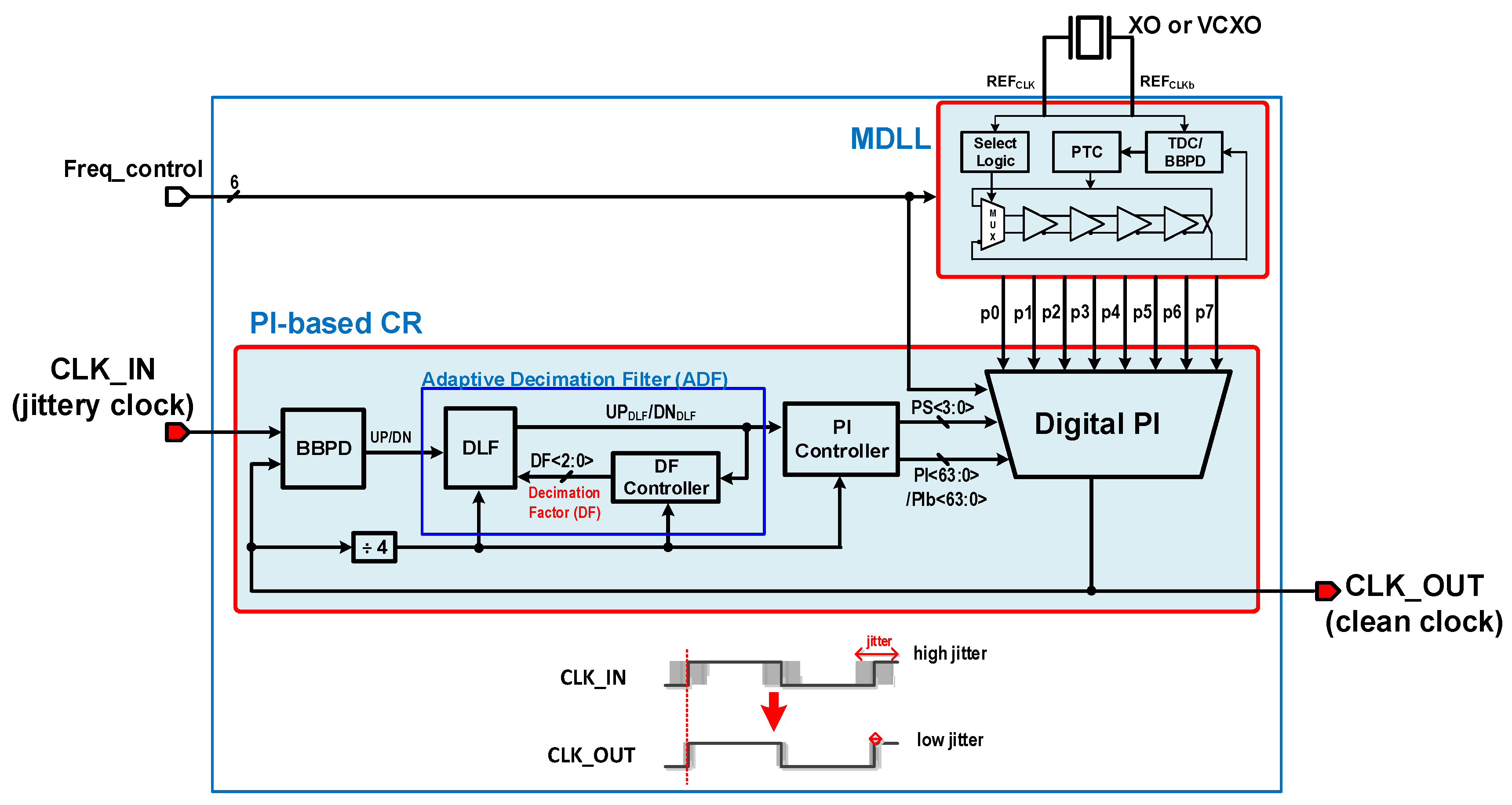
2. Proposed All-Digital Dual-Loop Jitter Attenuator (DJA)

2.1. Proposed DJA Architecture

Figure 3 shows a block diagram of the proposed all-digital dual-loop jitter attenuator (DJA) architecture. The proposed DJA is composed of a dual-loop structure: multiplying the delay-locked loop (MDLL) and the phase interpolator (PI)-based clock recovery (CR) loop. The first digital MDLL loop generates uniformly spaced, low-jitter eight-phase reference clocks (p0~p7) for the PI-based CR loop. The second PI-based CR loop is composed of a digital phase interpolator (PI), a bang-bang phase detector (BBPD), an adaptive decimation filter (ADF), a PI controller, and a 1/4 frequency divider. The ADF consists of a digital loop filter (DLF) and a decimation factor (DF) controller. The proposed DJA can clean the phase noise and jitter from the input clock (CLK_IN) and produce a low-jitter phase-aligned output clock (CLK_OUT). In the jitter attenuator of the proposed dual-loop structure, both the MDLL and PI-based CR are first-order systems, so the proposed DJA has the advantage of increased system stability. In addition, unlike general PLL-based jitter attenuators with a narrow frequency range and jitter peaking problems, the proposed DJA has the advantage of a wide operating frequency range without jitter peaking. The jittery input clock comes in with the phase edge continuously shifting back and forth slightly due to the jitter component. In the proposed DJA, the output signal of the BBPD does not directly drive the digital PI, but the decimation-filtered signal through the ADF is used for driving the PI. After this process, the output clock phase follows the average value of the input clock phase.
Figure 4 illustrates the dual-loop operation of the proposed DJA. In the proposed DJA, the first MDLL loop is activated at the beginning of the operation. Phase lock and frequency multiplication are performed quickly using the cyclic vernier time-to-digital converter (TDC). Then, using the delta-sigma modulator (DSM) for dithering jitter reduction in sequential tracking mode, N times multiplied low-jitter eight-phase output clocks (p0~p7) are generated. The 6-bit Freq_control signal adjusts the MDLL output frequency. After the MDLL loop is locked, the second PI-based CR loop starts to perform jitter and phase noise attenuating operations. The BBPD compares the jittery input clock (CLK_IN) with the output clock (CLK_OUT) of DJA and generates the UP/DN signal that informs the early or late phase information. The ADF generates the filtered output pulse signal UPDLF/DNDLF according to the coefficients of the decimation factor DF<2:0>. For example, when DF<2:0> = ‘001′ (DF = 4 in decimal), if the UP (or DN) pulse signal is accumulated four times, the UPDLF (or DNDLF) pulse signal is generated once. The PI controller then uses this UPDLF/DNDLF information to generate the octant selection signal PS<3:0> and the fine resolution signal PI<63:0>/PIb<63:0> needed to control the digital PI.
The proposed PI-based CR loop uses DF<2:0> = ‘000’ (DF = 1 in decimal) at the beginning of the operation to lock the output clock phase to the average frequency of the noisy input clock while maintaining the initial loop bandwidth. Then, decimation filtering [9,10,11] is performed while increasing the DF code sequentially from ‘000’ to ‘111’ in eight steps to lower the loop bandwidth to 1 K Hz or less. The structure of the proposed PI-based CR is similar to the general PI-based clock and data recovery (CDR). Therefore, Equation (1) below can determine the loop bandwidth of the proposed PI-based CR according to the DF code [12]. Here, Ø I N is the amplitude of the input sinusoidal jitter, Δ T is the minimum phase step of PI, DF is the decimation factor, and TFSM is the update period of PI.
Loop   Bandwidth     1 2 π · Ø I N · Δ T D F · T F S M
Table 1 shows the decimation factor coefficients in decimal according to the DF<2:0> codes.

2.2. Proposed Low-Jitter Eight-Phase All-Digital MDLL Frequency Multiplier

Figure 5a shows a block diagram of the proposed low-jitter eight-phase all-digital MDLL [13,14]. It consists of a phase tracking controller (PTC), an eight-phase digitally controlled oscillator (DCO), a slew control buffer, a select logic, and a programmable frequency divider (/N) with a division factor N of 24~47. The proposed MDLL has two operation modes: TDC tracking and sequential tracking. The PTC consists of a cyclic Vernier TDC, a BBPD, a digital loop filter (DLF), a delta-sigma modulator (DSM), and a binary-to-thermometer decoder. The eight-phase DCO consists of a four-stage delay line to generate eight-phase clocks (p0~p7) with a uniform phase interval of 45 degrees. The delay cell constituting each stage is a mux-based pseudo-differential structure with binary weighted varactors. Figure 5b shows the eight-phase clocks (p0~p7) of the MDLL operating at 2.4 GHz and 4.7 GHz, respectively. The maximum phase errors between the adjacent clocks were less than 1.3 and 1.6 degrees at 2.4 GHz and 4.7 GHz, respectively. Figure 5c shows the jitter simulation results of the proposed MDLL. It achieves a peak-to-peak (p-p) of 4.01 ps and a root mean square (RMS) jitter of 0.394 ps, respectively, at 4.7 GHz.
When the MDLL is turned on, the TDC tracking mode is first performed, and the TDC inside the PTC first measures the initial phase error between the REF and OUT signal using the cyclic Vernier TDC for fast locking operation. The DLF receives the 10-bit phase error information from the TDC and generates a 10-bit signal for controlling the DCO delay. The TDC tracking mode is completed within 100 ns, and the coarse phase lock is completed. After that, the TDC is turned off, and BBPD-based sequential tracking is started. At the beginning of sequential tracking, the DSM is turned off to reduce the residual phase error quickly, and then the DSM is turned on to minimize the dithering of jitter further [14]. The second-order DSM quantizes the 6-bit LSBs of the DLF output, and the binary-to-thermometer decoder generates control codes for adjusting the dithering cells of the delay cell.
The proposed MDLL multiplies the 100 MHz reference clock (REFCLK/REFCLKB) by N times (N = 24~47) to create 2.4~4.7 GHz wide-range eight-phase output clocks. The division factor N can be programmed with the 6-bit Freq_control signal. Since the designed MDLL operates in a wide frequency range from 2.4 GHz to 4.7 GHz, the reference clock’s rise time and fall time are finely adjusted using the slew control buffer, effectively reducing jitter. The proposed MDLL achieves a lock time of less than 400 ns.

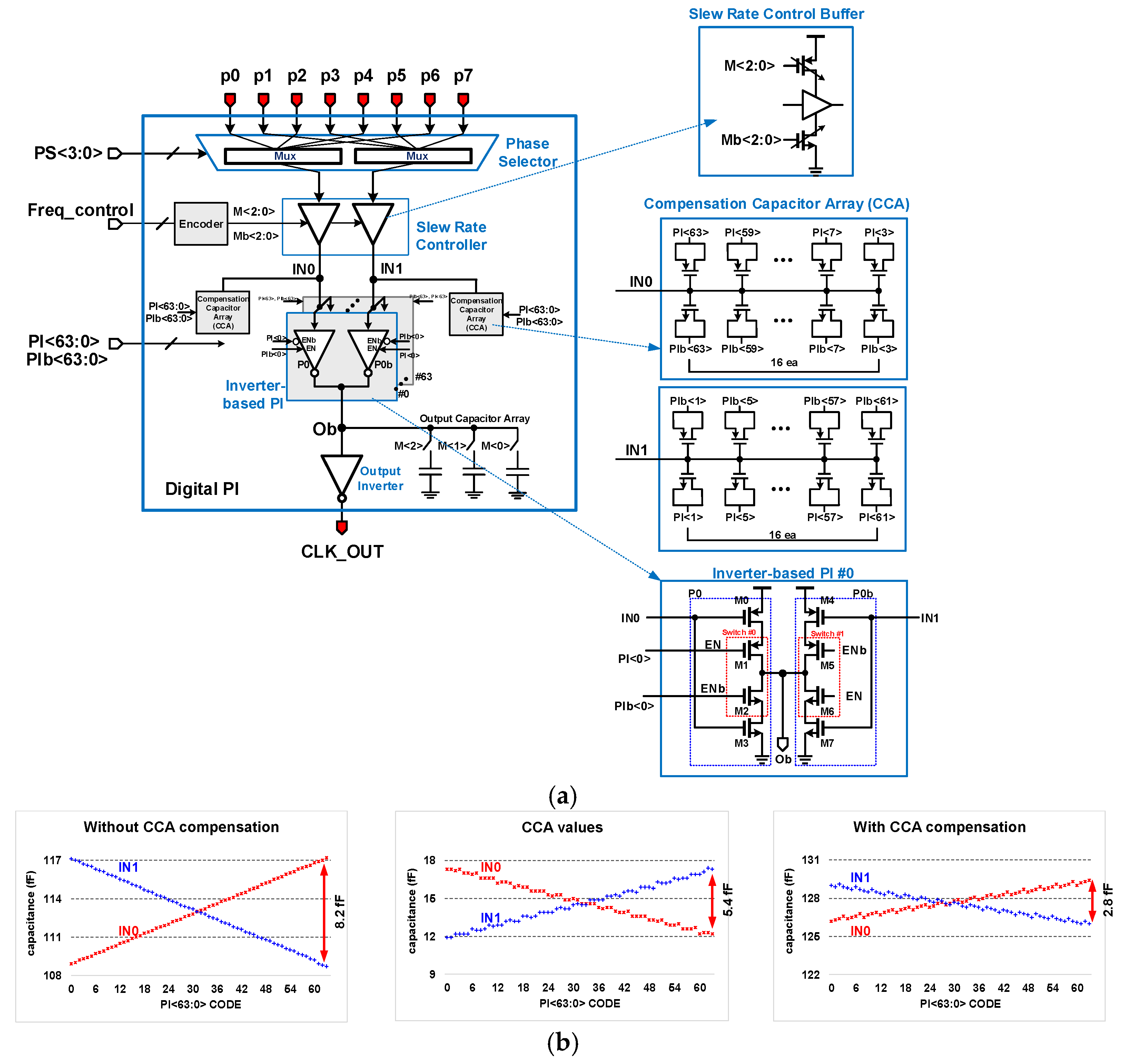
2.3. Proposed Digital PI

Figure 6a shows a block diagram of the proposed digital PI. The PI consists of a phase selector with two 4-to-1 multiplexers (MUX), a slew rate controller with two slew rate control buffers, two compensation capacitor arrays, 64 tri-state inverter-based PIs, an output capacitor array, and an output inverter. According to the PS<3:0> codes, the proposed PI selects two clock signals with a 45° phase difference among the eight-phase reference (p0~p7) inputs. Then, the CLK_OUT signal, whose phase step is controlled with a resolution of about 0.7° (=45°/26 = 0.415 ps at 4.7 GHz), is generated according to the PI<63:0> codes.
In the proposed PI, three compensation methods are applied to increase the linearity of the phase interpolation in the wide frequency range: First, a slew rate controller is used that can adjust the rise/fall times of the IN0/IN1 nodes according to the frequency range. When the frequency increases, the M<2:0> code value is changed to increase the driving ability of the slew rate control buffer, and vice versa, when the frequency decreases. Second, a compensation capacitor array (CCA) is used to compensate for the difference between the IN0 and IN1 node capacitance values that vary depending on the PI<63:0> code values. The reason for this compensation is that, referring to the lower right of Figure 6a, the input capacitance of the inverter-based PI may vary depending on the EN/ENb (=PI/PIb code) value controlling the intermediate switch transistors (M1, M2, M5, and M6). As shown on the left of Figure 6b, when there is no CCA, the capacitance of the IN0 node increases as the PI<63:0> code increases, but the capacitance of the IN1 node decreases inversely. Here, the maximum capacitance difference between the IN0 and IN1 nodes is about 8.2 fF. To compensate for the capacitance difference between these two nodes, as shown in the middle of Figure 6b, switched compensation capacitor arrays (CCAs) that can reduce (IN0 node) or increase (IN1 node) the node capacitance value according to the PI<63:0> codes are connected to the IN0 and IN1 nodes, respectively. On the right side of Figure 6b, it can be seen that the maximum difference between IN0 and IN1 node capacitance is significantly reduced from 8.2 fF to 2.8 fF by using the CCA compensation method. Third, an output capacitor array is used to adjust the slew rate of the output node (Ob) according to the frequency range. When the frequency increases, the M<2:0> code value is reduced to block the connection paths between the Ob node and the output capacitor array. Conversely, if the frequency decreases, the connection path between the Ob node and the output capacitor array increases, thereby increasing the Ob node capacitance.
Figure 7 illustrates the phase interpolation method of the proposed 9-bit PI with 512 (=29) steps. The resolution of the proposed digital PI is about 0.7 degrees. Figure 8 illustrates the post-layout simulation results of the proposed digital PI showing the INL and DNL of the PI. It can be seen that INL is significantly reduced from 2.638 LSB to 0.829 LSB using the proposed three compensation methods.

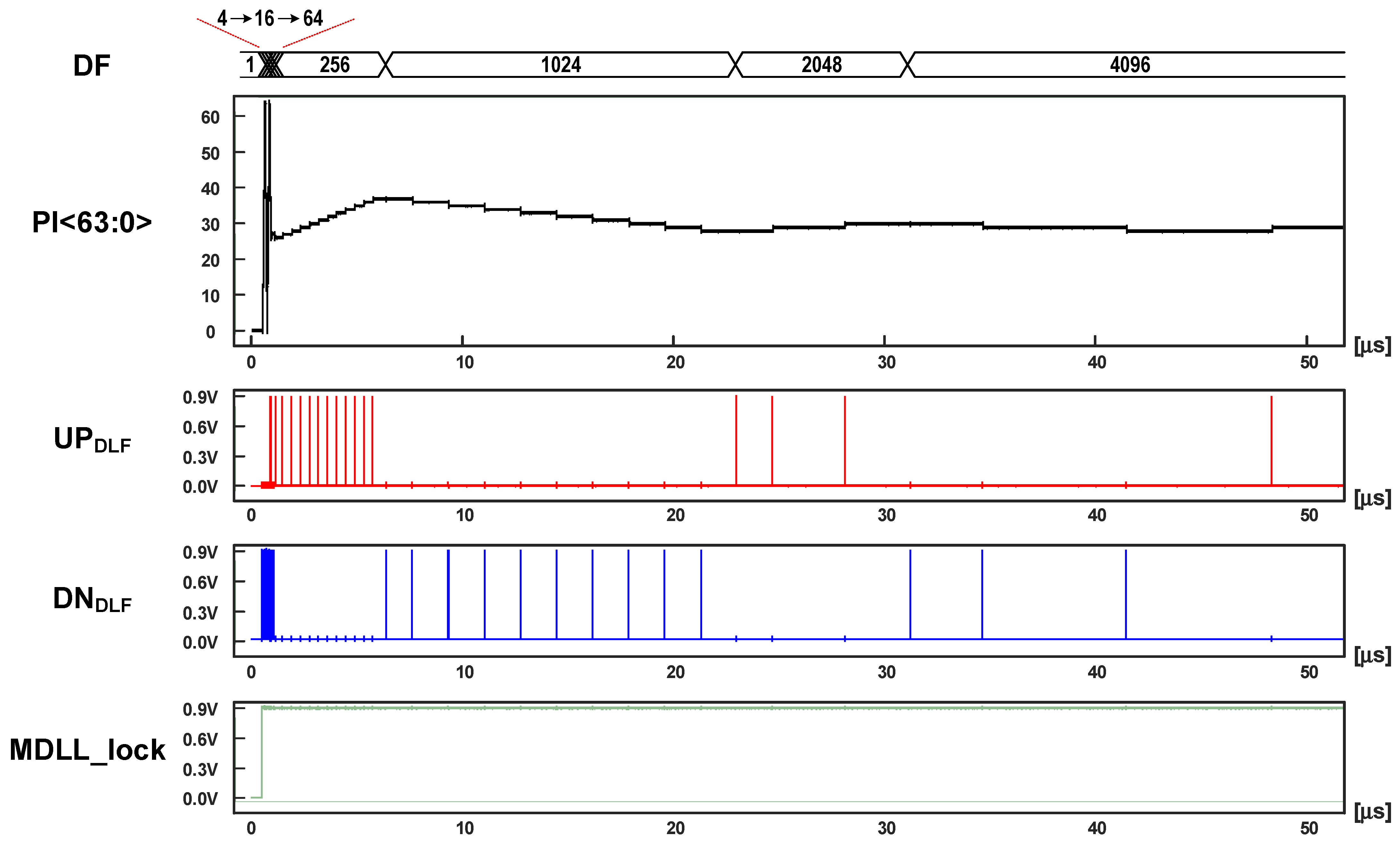
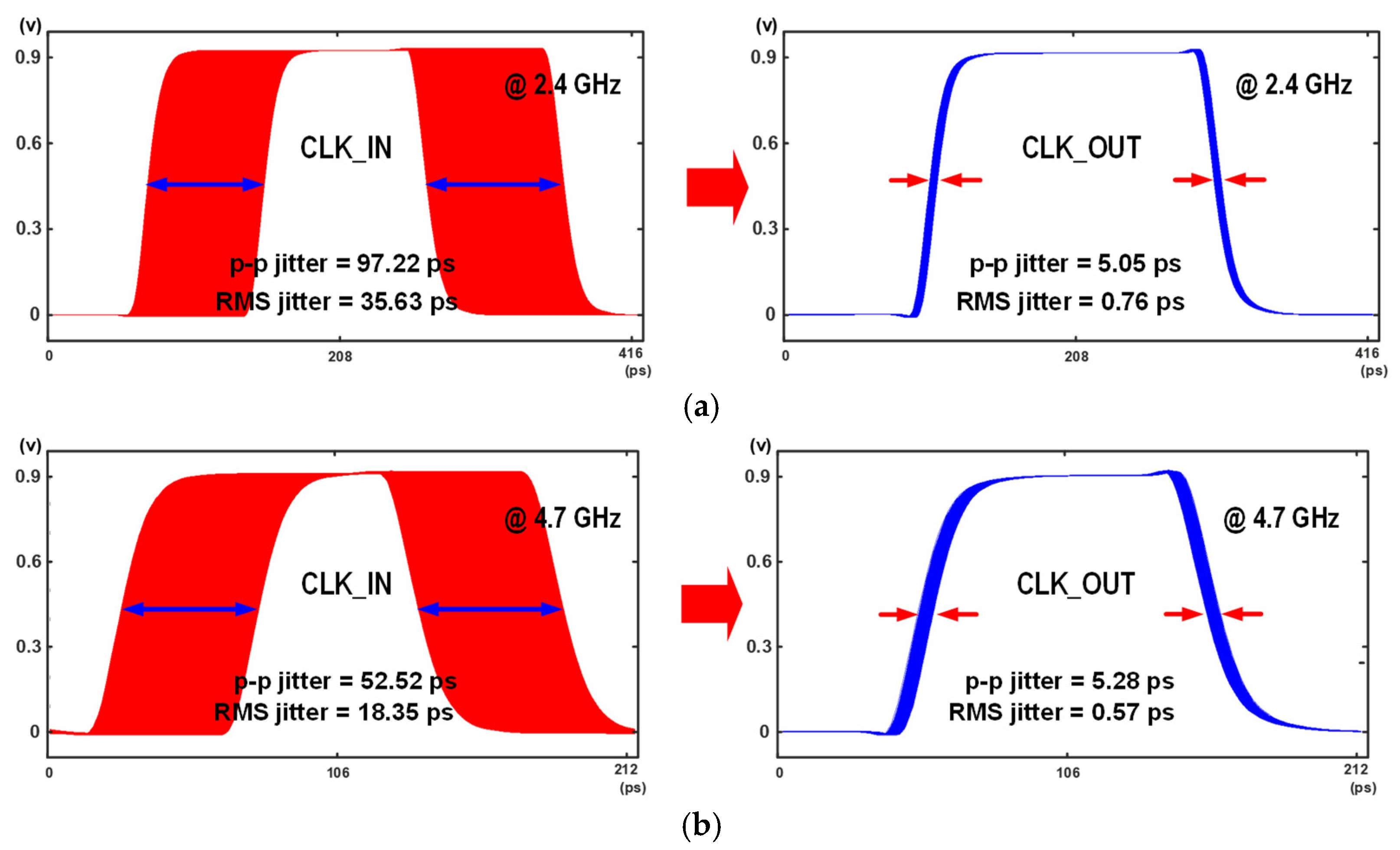
3. Experimental Results

The proposed all-digital DJA was implemented in a 40 nm CMOS process. Figure 9 shows the chip layout of the proposed DJA, where the active core area is only 174 µm × 148 µm = 0.0257 mm2. The proposed DJA achieves a programmable operating frequency range of 2.4~4.7 GHz. The DJA consumes 11.48 mW at 4.7 GHz. As a result, the proposed DJA effectively removes undesired input clock jitter noise and produces an ultra-low jitter output clock.
Figure 10 shows the post-layout simulated locking process of the proposed all-digital DJA at 2.4 GHz. At the beginning of the operation, the MDLL is locked quickly to create eight frequency-multiplied reference clocks. After that, the DJA starts adaptive decimation filtering, and the DF value is sequentially increased up to 4096 whenever the polarity of the DLF output (UPDLF/DNDLF) value changes (DF in decimal: 1→4→256→1024→2048→4096).
Figure 11 shows the jitter transfer simulation results of the proposed DJA. This is the simulation result of DJA modeled using Xmodel, one of the SystemVerilog simulators [15]. When the amplitude of the input sinusoidal jitter is 0.1 UI at the operating frequencies of 2.4 GHz and 4.7 GHz, respectively, it can be seen that the loop bandwidth of the proposed DJA is significantly reduced as the DF value increases. When DF = 4096, the approximate loop bandwidth is as low as 0.77 KHz at 2.4 GHz and 1.53 KHz at 4.7 GHz, respectively.
Figure 12 shows the post-layout simulation results of the proposed DJA operating at 2.4 GHz and 4.7 GHz, respectively. As shown in Figure 12a, when the noisy 2.4 GHz input clock (CLK_IN) has a p-p period jitter of about 97 ps (=0.233 UI) from a 25 KHz sinusoidal input jitter, the proposed DJA generates the clean output clock (CLK_OUT) with a jitter value as small as 5.05 ps (=0.012 UI) at 2.4 GHz. Figure 12b shows that the noisy 4.7 GHz clock with a high p-p period jitter of about 97 ps (=0.242 UI) from a 50 KHz input sinusoidal jitter is filtered and reduced to 5.28 ps (=0.024 UI) after passing through the DJA. Figure 13 shows the post-layout-based phase noise simulation (Synopsys FineSim) plots at 2.4 GHz output frequency. At the output clock frequency of 2.4 GHz, the noisy RMS jitter is reduced from 20.86 ps to 482.6 fs, showing a jitter reduction of about –32.6 dB. At 4.7 GHz, the jitter attenuation performance is about –31.8 dB. Table 2 summarizes the performance of the proposed all-digital DJA. The performance in this design is the post-layout-based FineSim simulation results.

4. Conclusions

In this paper, a new all-digital jitter attenuator featuring a digital PI-based CR and a multi-phase MDLL for low-cost BOT-based parallel multi-DUT testing is presented. By utilizing a new adaptive decimation filter (ADF) technique, the proposed DJA achieves an RMS jitter attenuation of more than –30 dB in the operating range of 2.4 GHz to 4.7 GHz. The proposed jitter attenuator was implemented in a 40 nm 0.9 V CMOS process, which occupies an active area of only 0.0257 mm2 and consumes 11.48 mW at 4.7 GHz. The proposed DJA can be a cost-effective and compact solution to replace the conventional PLL-based jitter cleaners in parallel testing systems and high-speed SoC design areas that require jitter and phase noise cleaning of the input clock.

Author Contributions

Conceptualization, J.K.; methodology, J.K., S.K. and J.J.; validation, J.K. and S.K.; formal analysis, J.K. and S.K.; investigation, J.K.; writing—original draft preparation, S.K; writing—review and editing, J.K.; supervision, J.K.; project administration, J.K.; funding acquisition, J.K. All authors have read and agreed to the published version of the manuscript.

Funding

This work was supported by the Korea Institute for Advancement of Technology (KIAT) grant funded by the Korea Government (MOTIE) P0020966. This work was also supported by the National R&D Program through the National Research Foundation of Korea (NRF) funded by the Ministry of Science and ICT (2022M3I8A1077243). The EDA tools were supported by IDEC.

Conflicts of Interest

The authors declare no conflict of interest.

References

  1. Adachi, T.; Pramanick, A.; Elston, M. Parallel, multi-dut testing in an open architecture test system. In Proceedings of the IEEE International Conference on Test, Austin, TX, USA, 8 November 2005; p. 9. [Google Scholar]
  2. Farayola, P.O.; Chaganti, S.K.; Obaidi, A.O.; Sheikh, A.; Ravi, S.; Chen, D. Detection of site to site variations from volume measurement data in multisite semiconductor testing. IEEE Trans. Instrum. Meas. 2021, 70, 1–12. [Google Scholar] [CrossRef]
  3. Park, J.; Lee, J.W.; Chung, J.; Han, K.; Abraham, J.A.; Byun, E.; Woo, C.J.; Oh, S. At-speed test of high-speed dut using built-off test interface. In Proceedings of the 2010 19th IEEE Asian Test Symposium, Shanghai, China, 1–4 December 2020; pp. 269–274. [Google Scholar]
  4. Lee, Y.; Lee, Y.W.; Seo, S.; Kang, S. Reduced-pin-count BOST for test-cost reduction. IEEE Trans. Comput.-Aided Design Integr. Circuits Syst. 2022, 41, 750–761. [Google Scholar] [CrossRef]
  5. Moon, J.W.; Yoo, H.S.; Choi, H.; Park, I.W.; Kang, S.Y.; Kim, J.B.; Chung, H.; Kim, K.; Lee, D.H.; Song, K.J.; et al. An enhanced built-off-test transceiver with wide-range, self-calibration engine for 3.2 Gb/s/pin DDR4 SDRAM. In Proceedings of the 2018 IEEE Asian Solid-State Circuits Conference (A-SSCC), Tainan, Taiwan, 5–7 November 2018; pp. 139–142. [Google Scholar]
  6. Slightom, K. Dual-loop clock generator cleans jitter, provides multiple high-frequency Outputs. Analog Dialogue 2014, 48, 15. [Google Scholar]
  7. Texas Instruments, LMK04208 Low-Noise Clock Jitter Cleaner with Dual Loop PLLs. Available online: https://www.ti.com/lit/gpn/lmk04208 (accessed on 20 October 2022).
  8. Khoo, C.L.; How, H.C.; Lo, W.W.; Wong, M.O. Low cost clock cleaner solution for reference clock sources. In Proceedings of the 2009 1st Asia Symposium on Quality Electronic Design (ASQED), Kuala Lumpur, Malaysia, 15–16 July 2009; pp. 194–198. [Google Scholar]
  9. Chiueh, L.H.; Lee, T.C. A 6-Gb/s adaptive-loop-bandwidth clock and data recovery (CDR) circuit. In Proceedings of the 2014 IEEE Asian Solid-State Circuits Conference (A-SSCC), Kaohsiung, Taiwan, 10–12 November 2014; pp. 289–292. [Google Scholar]
  10. Zheng, X.; Zhang, C.; Yuan, S.; Zhao, F.; Yue, S.; Wang, Z.; Li, F.; Wang, Z. An improved 40 Gb/s CDR with jitter-suppression filters and phase-compensating interpolators. In Proceedings of the 2014 IEEE Asian Solid-State Circuits Conference (A-SSCC), Toyama, Japan, 7–9 November 2016; pp. 85–88. [Google Scholar]
  11. Wu, G.; Huang, D.; Li, J.; Gui, P.; Liu, T.; Guo, S.; Wang, R.; Fan, Y.; Chakraborty, S.; Morgan, M. A 1–16 Gb/s All-digital clock and data recovery with a wideband high-linearity phase interpolator. IEEE Trans. Very Large Scale Integr. (VlSI) Syst. 2016, 24, 2511–2520. [Google Scholar] [CrossRef]
  12. Hanumolu, P.K.; Wei, J.K.; Moon, U.K. A wide-tracking range clock and data recovery circuit. IEEE J. Solid-State Circuits 2008, 43, 425–439. [Google Scholar] [CrossRef] [Green Version]
  13. Kim, J.; Han, S. A fast-locking all-digital multiplying DLL for fractional-ratio dynamic frequency scaling. IEEE Trans. Circuits Syst. II Express Briefs 2018, 65, 276–280. [Google Scholar] [CrossRef]
  14. Park, D.; Kim, J. A low-jitter 2.4 GHz all-digital MDLL with a dithering jitter reduction scheme for 256 times frequency multiplication. IEICE Electron. Express 2020, 17, 20200296. [Google Scholar] [CrossRef]
  15. Choi, N.; Kim, J. Modeling and simulation of NAND flash memory sensing systems with cell-to-cell Vth variations. In Proceedings of the 39th International Conference on Computer-Aided Design (ICCAD), Virtual Event, San Diego, CA, USA, 2–5 November 2020; pp. 1–8. [Google Scholar]
Figure 1. Simplified block diagram of a BOT-based parallel multi-DUT test system.
Electronics 11 03630 g001
Figure 2. (a) Conventional PLL-based clock jitter attenuator. (b) Simplified block diagram of a wide-range jitter attenuator architecture using multiple PLLs.
Electronics 11 03630 g002
Figure 3. Proposed all-digital dual-loop jitter attenuator (DJA) architecture.
Electronics 11 03630 g003
Figure 4. Flowchart illustrating the dual-loop operation of the proposed all-digital DJA.
Electronics 11 03630 g004
Figure 5. (a) Proposed low-jitter eight-phase all-digital MDLL, (b) eight-phase output clocks of the MDLL, and (c) post-layout-based jitter simulation performance of the proposed all-digital MDLL.
Electronics 11 03630 g005aElectronics 11 03630 g005b
Figure 6. (a) Proposed digital PI. (b) N0/N1 node capacitance compensation using the compensation capacitor array (CCA).
Electronics 11 03630 g006
Figure 7. Phase interpolation method of the proposed 9-bit PI with 512 (=29) steps.
Electronics 11 03630 g007
Figure 8. Post-layout corner simulation results of the proposed digital PI showing the INL and DNL of the PI, with and without the proposed compensation methods.
Electronics 11 03630 g008
Figure 9. Chip layout of the proposed all-digital DJA.
Electronics 11 03630 g009
Figure 10. Post-layout simulated locking process of proposed DJA.
Electronics 11 03630 g010
Figure 11. Simulated jitter transfer simulation results at 2.4 GHz and 4.7 GHz.
Electronics 11 03630 g011
Figure 12. Post-layout simulation results of the proposed DJA showing input and output clock jitter eye diagram at (a) 2.4 GHz and (b) 4.7 GHz.
Electronics 11 03630 g012
Figure 13. Post-layout-based phase noise simulation plots at 2.4 GHz output frequency.
Electronics 11 03630 g013
Table 1. Decimation factor (DF) coefficients according to DF<2:0> codes.
DF<2:0> CodeDecimation Factor (DF) Coefficients
(in Decimal)
0001
0014
01016
01164
100256
1011024
1102048
1114096
Table 2. Performance table of the proposed all-digital DJA.
Reference[6][7]This Work
TechnologyNANA40 nm CMOS
Supply voltage (V)3.33.30.9
ArchitectureAnalog
PLL-based
Analog
PLL-based
All Digital
PI-based
Operating frequency (GHz)3.6–4.02.75–3.0722.4–4.7
Settling time (μs)NANA<50
Loop bandwidth (Hz)10–10010–2001530 @ 4.7 GHz
770 @ 2.4 GHz
External loop filter capacitorRequiredRequiredNot Required
RMS jitter performance (fs)<200 1111 1330.1 2 @ 4.7 GHz
482.5 2 @ 2.4 GHz
Power consumption (mW)389 3419 3Total: 11.48 @ 4.7 GHz
(MDLL: 6.4, PI-based CR: 5.08)
Active core area (mm2)NANA0.0257
1 12 KHz to 20 MHz RMS jitter integration, 2 35 KHz to 50 MHz RMS jitter integration, 3 includes LDO and clock driver power.
Publisher’s Note: MDPI stays neutral with regard to jurisdictional claims in published maps and institutional affiliations.

