1. Introduction
A thermoelectric generator (TEG) is a device generating electric power based on temperature differences, which is known as the Seebeck effect [
1,
2,
3]. A TEG is a key device for energy harvesting among many alternatives such as photovoltaic generators and electrostatic, electromagnetic, magnetostrictive or piezoelectric vibration devices [
4]. Given that a nominal TEG can only generate an output voltage on an order of 10–100 mV with a few K temperature difference, a power converter is needed to operate integrated circuits (ICs) including sensor and RF at a higher voltages such as 3 V in autonomous sensor modules [
5,
6,
7,
8,
9], as shown in
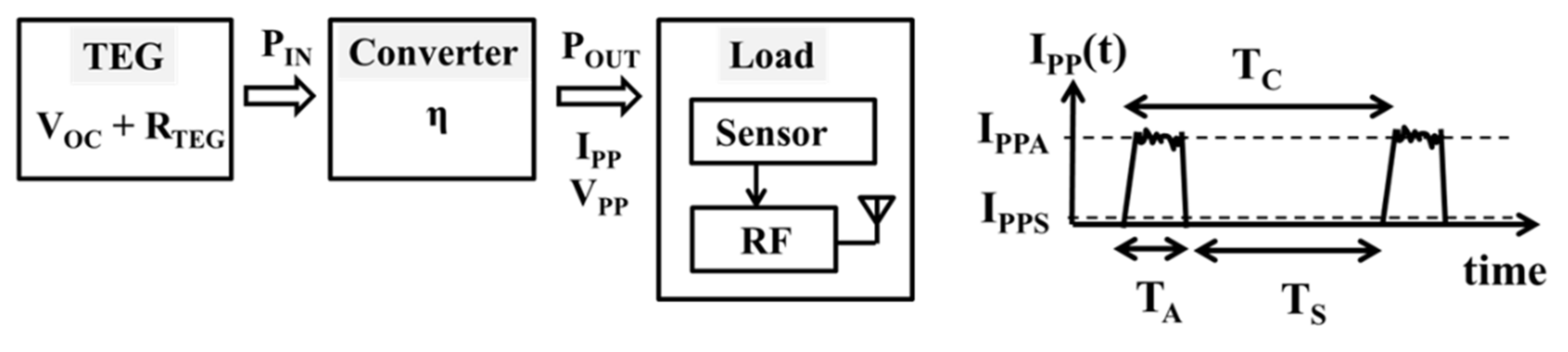
Figure 1, where
VOC (
RTEG) is the open circuit voltage (output resistance) of TEG,
η is the power conversion efficiency of the converter, and
VPP (
IPP,
POUT) is the output voltage (average output current, average output power) of the converter to drive sensor and RF blocks.
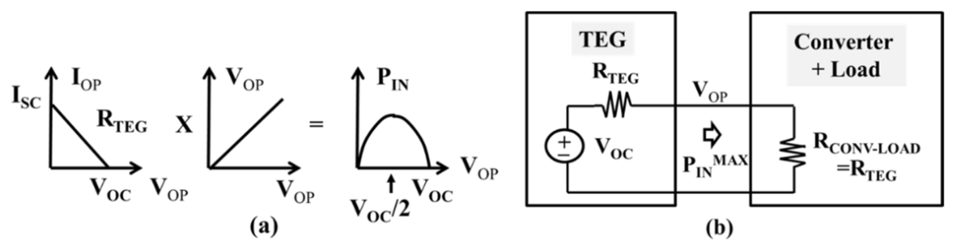
Characteristics of the output current (
IOP) and voltage (
VOP) of TEGs are described in
Figure 2a with an equivalent circuit with
VOC and
RTEG as shown in
Figure 2b, where
ISC is the short circuit current of the TEG and
PIN is the output power of the TEG or the input power of the converter.
As a result,
PIN is described by a parabola where the peak power is given at the interface voltage
VOP =
VOC/2. Based on the equivalent circuit of a TEG system as shown in
Figure 2b, the converter is designed to operate TEG at the maximum power point with a given
IOP-
VOP characteristic of TEG [
10,
11]. When TEG cannot operate at the maximum power point due to low input voltage, the converter needs to control the input voltage as well as the output voltage [
12]. Once the application is determined, the required output current of the converter (
IPP) can be estimated by using (1),
where
IPPA,
TA,
IPPS,
TS, and
TC are an average current in operation, an operation period per sense and data transmission, an average stand-by current, a stand-by period, and a cycle time per operation, respectively, as shown in
Figure 1. Note that a rechargeable battery or a large capacitor is usually connected at the input terminal of the loading device to stabilize the input voltage of the sensor/RF IC against large
IPPA.
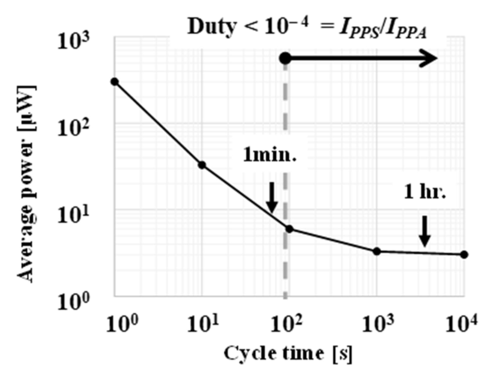
Figure 3 shows the average power as a function of
TC in case of
VPP of 3 V,
IPPS of 1 μA,
IPPA of 10 mA, a bit rate of 1 Mbps, and 1 k-bytes/packet with Bluetooth low energy [
13]. At a duty of 10
−4 or lower,
IPP can be as low as 10 μW. Thus, the requirement for the output power of the converter is determined. From a system viewpoint, one may want to design a TEG structure in such a way that the output power of the converter is maximized under a given load condition.
Table 1 illustrates a TEG composed of multiple pairs of n- and p-type thermocouples (TC).
NS (
NP) is the number of TCs connected in series (parallel). In this example, 8 TCs are connected in series (a) or arranged with two arrays of 4 TCs serially connected (b). The former configuration has higher
VOC and larger
RTEG than the latter does, as shown by (a) and (b) of
Figure 4.
Thus, even though the area is given, one has a degree of freedom in a combination of
NS and
NP while the multiple of them is constant. In [
14], a design technique was proposed to extract the maximum power over a wide
VOC range in case of a lack of converter by varying a combination of
NS and
NP. However, to the author’s knowledge, there have been no design considerations for TEG with converters under given load conditions in the literature to answer the question of how one can determine
NS and
NP under given system conditions. For example, as shown in
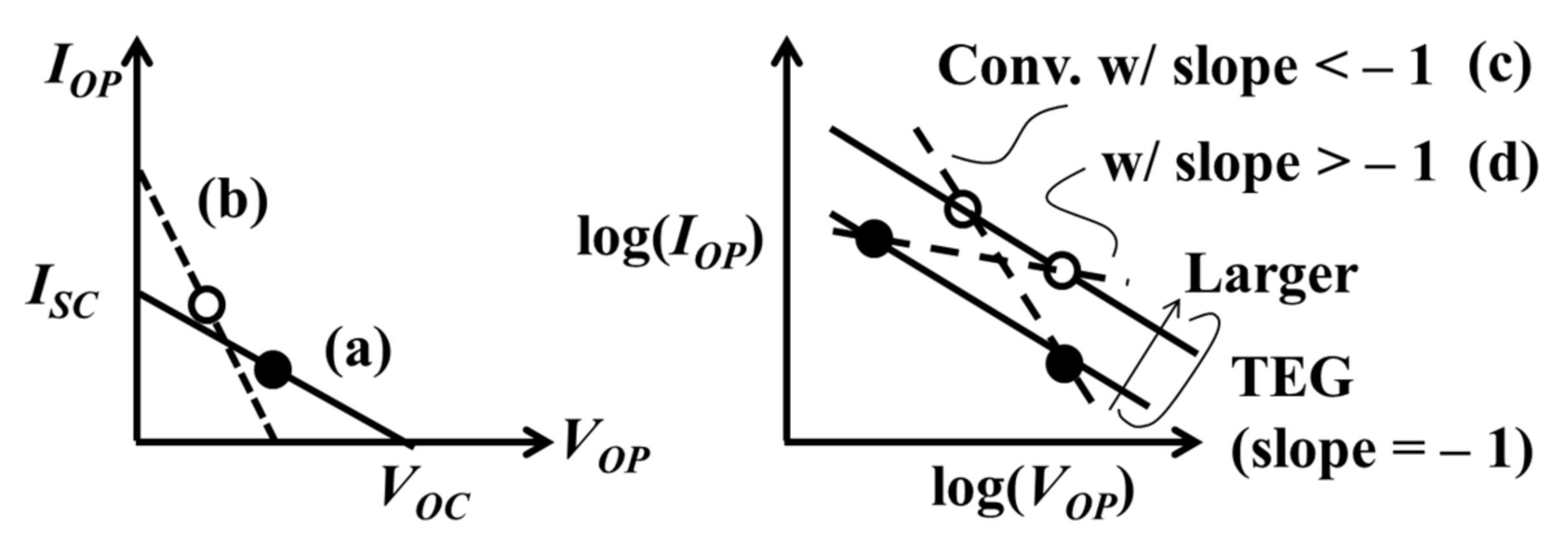
Figure 4, the operating point given by the cross point of the
VOP −
IOP curves for the TEG and the converter depends on the slope of the
VOP −
IOP curve for the converter of smaller (c) or larger (d) than −1. Since TEG is one of the most significant devices in terms of sensor module cost, its size or area must be minimized to enable massively distributed sensor modules.
This paper discusses a relationship between TEG electrical parameters, power efficiency of the converter, and power of the load toward minimizing TEG cost. How
VOC or
RTEG should be determined is shown. In addition, a design flow is proposed to minimize TEG area when the load condition is given, a Dickson charge pump (CP) [
15] as converter is used to be integrated in the sensor, with an RF chip as a cost-effective solution.
2. Equations between TEG, Converter, and Load
By definition, as described in
Figure 1,
To extract power from TEG as much as possible, the converter needs to be operated to match the input impedance of the converter with the output impedance of TEG for impedance matching, as illustrated in
Figure 2b. Under the maximum-output-power condition,
PIN is given by (3).
From (2) and (3), TEG device parameters and circuit parameters are related by (4).
VOC is proportional to Δ
T [
2].
VOC and
RTEG can be varied proportionally by changing TEG structure as described in
Table 1. As a result, when specific TCs are characterized,
VOC and
RTEG are related as in (5).
where
VTC and
RTC are an open circuit voltage and an output impedance of a TC, respectively. The area of TEG can be estimated by the area of TC (
ATC) from (5),
VOC can be also shown with
RTEG, instead of
NS from (5), as below.
Finally, TEG with minimum area and the maximum operating point are determined by the filled circle rather than the blank one on the curve (c) or (d) in
Figure 4, depending on the converter characteristic with a slope of <−1 or >−1. A trajectory of the maximum power point of TEG with a given area on log(
IOP) − log(
VOP) plane has a slope of −1. The trajectory of smaller TEG becomes closer to the origin. When the converter has a slope of <−1 as described by the curve (c) in
Figure 4, the maximum power point is located at a relatively higher
VOP and a relatively lower
IOP than the case of using a converter whose slope is greater than −1.
Several conditions for TEG design are studied as follows. When the TEG area and structure are given,
VOC can be varied only by increasing Δ
T. The minimum Δ
T is determined by (4).
VOC depends on the square root of
VPP,
IPP,
RTEG, and
η. Among them,
VPP and
η are expected to not change significantly, at least in a short term.
Figure 5 shows
VOC vs.
η with
IPP = 30 μA or 3 μA and
RTEG = 300 Ω or 1 kΩ at
VPP = 3 V based on (4). When
η is nominally 50%, an improvement in
η by 10% only gives 10% reduction in
VOC. Similar goes to
VPP. As a result, it is considered that
VPP and
η are not effective design parameters to mitigate the requirement for reducing
VOC.
On the other hand, when applications allow 10X longer cycle time as shown in
Figure 3, the required
VOC can be significantly reduced, resulting in reduction in TEG cost with reduced
NS. Next, let’s look at the relationship between
VOC and
RTEG when
η and the load condition are assumed.
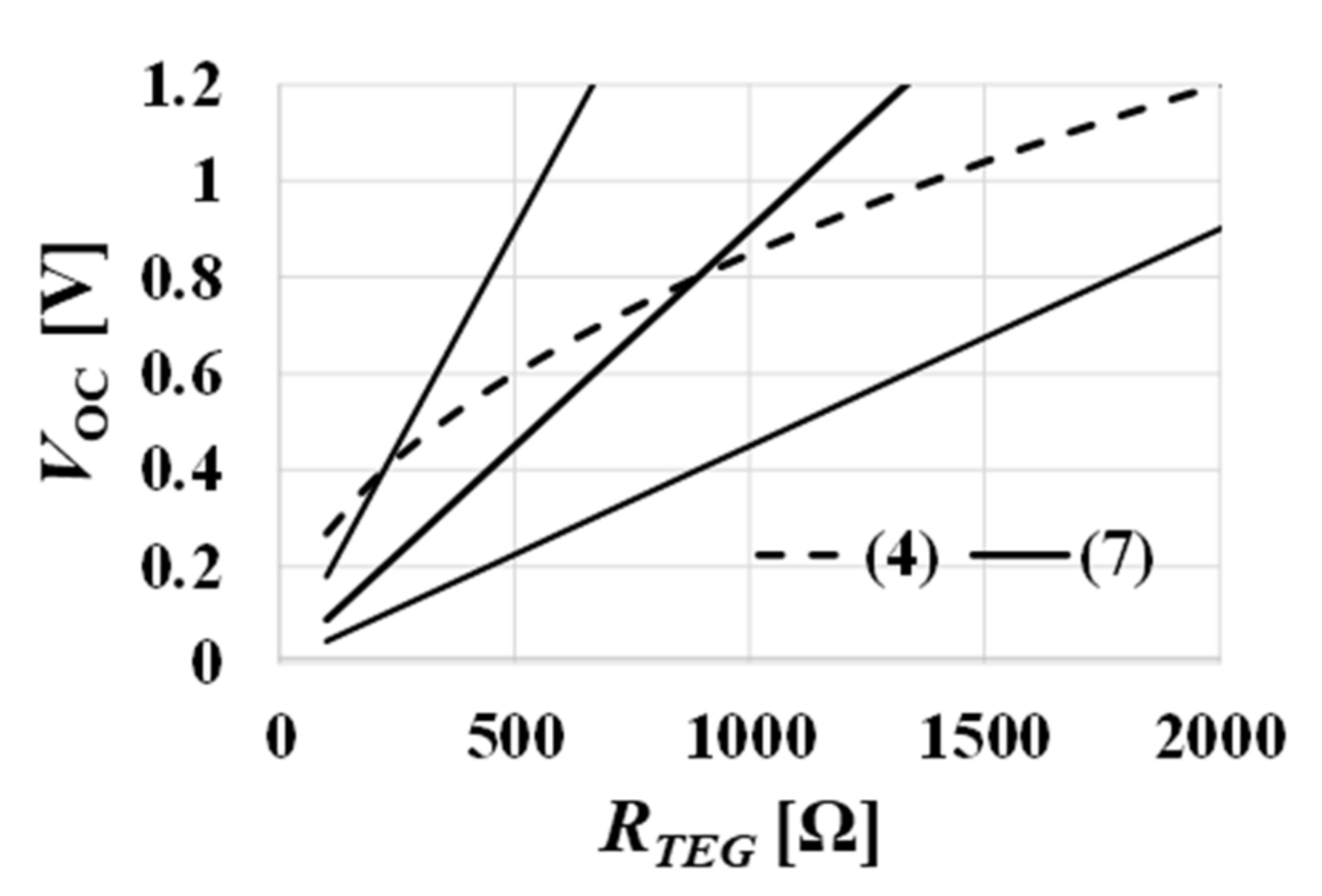
Figure 6 shows
VOC vs.
RTEG with different
IPP,
η = 0.5,
VPP = 3 V, based on (4). If
RTEG needs to increase for small form factor by a factor of 10,
VOC has to increase by a factor of 3.2. Alternately, if
TC can be relaxed by a factor of 10 by reducing the frequency of sense and data transmission to 1/10 in a certain application,
IPP can decrease by a factor of 10, which allows the system to work with
VOC unchanged.
How can one determine
RTEG when
VOC is limited by the minimum operation voltage of the converter
VDDMIN?
Figure 7 shows
RTEG vs.
IPP with
VOC = 0.4 V or 0.8 V,
η = 0.5,
VPP = 3 V. Even if
VDDMIN of the converter can be reduced from
VOP =
VOC/2 = 0.4 V in case of
VOC = 0.8 V to
VOP = 0.2 V with converter designers’ effort,
RTEG also has to be reduced by a factor of 4 with the same Δ
T and
IPP, or
IPP also has to be reduced by a factor of 4 with the same Δ
T and
RTEG, instead. Thus, the effort of improving the converter with respect to reduction in
VDDMIN requires more effort of reducing
RTEG for TEG designers or of reducing
IPP for system designers.
Figure 8 shows a relationship between (4) and (7). The cross points of them express the values of
RTEG and
VOC for a given condition of
VTC/
RTC = 0.45 mA,
IPP =30 μA,
η = 0.5,
VPP = 3 V. Given that
η is assumed to be constant over
VOP for simplicity in this section, one cannot determine
NS and
NP to minimize TEG area. Therefore, in order to design TEG with minimum cost, a converter needs to be optimally designed by
VOP precisely.
3. Design Flow of TEG with Minimum Area
In the above section II, η was assumed to be constant to overview the relationship between TEG electrical characteristics, converter power efficiency, and the load condition of the sensor module. In this section, a more practical design flow is proposed to determine both NS and NP of TEG and the design parameters of CP whose η can vary as VOP at the same time.
(Assumption) The following parameters are given: VTC, RTC, and the target IPP_TGT at VPP.
(Parameters to be determined) NS, NP, in such a way that TEG area, i.e., the product NS NP, is minimum, as well as the number of stage NCP, capacitance per stage CCP and clock frequency fCP to design CP.
(Step 1) Design CP with the maximum power conversion efficiency for each
VOP when the target
IPP is given at a specific
VPP, based on [
16] as below.
It is assumed that (1) CP to be designed is a Dickson type [
15], (2) it operates in slow switching limit (SSL) where the clock frequency is low enough to transfer the charges from one stage to the next one through a switching MOSFET in the subthreshold region or namely a switching diode, a unit of the diode has a voltage(
VD)–current(
ID) relationship specified by (8), and the oscillator cell consumes much lower power than the CP. Design flow in fast switching limit is open for the future work.
The output voltage(
VOUT)–current(
IOUT) relationship of the CP is given by (9) where the output impedance
RPMP and the maximum attainable voltage
VMAX are given by (10) and (11), respectively. The top plate parasitic capacitance
is assumed to be given by (12), where N
D, A
D, and C
J are the number of unit diodes, the junction area of a unit diode, and the junction capacitance of a unit diode.
VTHEFF is an effective threshold voltage given by (13) [
17], which is defined by the voltage difference between the adjacent capacitors at the negative clock edge, indicating the voltage loss per stage.
The input current
IOP of the CP is given by (14) as a function of the output current
IPP and the input voltage
VOP. The last term comes from the reverse leakage of switching diodes.
The power conversion efficiency is defined by (15).
The optimum number of stages
NOPT to maximize the power efficiency is estimated by (16) using the minimum number of stages to output
VPP with zero output current given by (17) [
18,
19], where [X] indicates a rounded integer number of X.
CP design flow starts with an initial condition on the target IPP_TGT at VPP, VOP, CP area ACPINIT. IPP and VPP are specified by the loading devices such as sensor and RF ICs. The goal is determining the TEG configuration and the circuit parameters of the CP such that TEG and CP areas are minimized.
Consequently,
ND and
VTHEFF are treated as variables. One can calculate the flowing parameters step by step:
NMIN by (17),
NOPT by (16),
CCP by (18), and
by (12). It is assumed in (18) that the CP area is occupied by the capacitors and switching diodes, where
COX is the capacitance density of each capacitor.
One can numerically solve (13) for
fCP because the remaining parameters are determined. From (10) and (11),
RPMP and
VMAX are calculated. Then,
IPP is determined by (19).
When
IPP is not equal to
IPP_TGT,
CCP and
ND need to be scaled up or down by the scaling factor
SF given by (20). When both
CCP and
ND are scaled proportionally, the optimum
fCP can stay the same value because (13) has
CCP and
ND only as their ratio. Thus, the required CP area to output
IPP_TGT at
VPP is determined by (21).
This flow can be done with various combinations of VTHEFF and ND. One can determine the best combination of all the CP parameters such as VTHEFF, ND, NCP, CCP, and fCP to have the maximum η for a given VOP. One then needs to repeat the above procedure for various VOP. The resultant VOP − IOP and VOP − ACP curves will be used together with those for TEG to determine the target configurations of TEG and CP with minimum areas as presented below.
(Step 2)
2-1: When
VOP <
VOC_MAX/2 where
VOC_MAX is
VOC with
NP = 1, find the operating point (
VOP,
IOP) in such a way that
VOC = 2
VOP and
RTEG =
VOP/(2
IOP) which meets the maximum power condition (3), as shown by the line (a) in
Figure 9.
Then,
ATEG is estimated by (23), based on (6).
2-2: When
VOP >
VOC_MAX/2, one cannot design TEG to run at the maximum operating point even with
NP = 1, as shown by the line (b) in
Figure 9. Instead, TEG needs to have the following parameters:
Then,
ATEG is estimated by (25), based on (6).
where
NS and
NP are given by (26).
(Step 3) Find VOP to minimize ATEG among the values found in Step 2 in the VOP range. One can also determine the design parameters of CP such as NCP, CCP, and fCP at the same time.
Let’s see how the above flow works using the parameters in
Table 2, which were presented in [
16], for demonstration.
Figure 10a–e show
η vs. CP area when
VTHEFF is varied between 0.02 V and 0.15 V and
ND is varied among 10, 30, 100, 300, 1000 at
VOP of 1.25 V in (a) through 0.25 V in (e), respectively. In this work,
η is the highest priority, but a very strict constraint could need too large a CP area. Considering a trade-off between
η and CP area, the best combination of the CP design parameters is determined, in order to have 2% lower
η than its peak value, which is shown by an arrow in each figure. There were two groups in
Figure 10b. One has
η > 0.55 and the other has
η < 0.5. The former has
NCP of three whereas the latter has
NCP of four. As
VOP decreases, the number of groups with different numbers of
NCP increases. Smooth variations on
η—CP area curves come from variations in
VTHEFF or
ND while
NCP is unchanged.
Figure 11 show how smooth the functions of
η,
fCP, CP area over
ND and
VTHEFF are when
VOP is 0.25 V.
VTHEFF is 0.03 V in
Figure 11a–c.
ND is 30 in
Figure 11d–f. The arrows in
Figure 11a,c indicate the optimum design plotted in
Figure 10e. As
ND increases, CP can run faster to keep
VTHEFF, as shown in
Figure 11b. To obtain a target output current at a target output voltage, capacitors can be scaled with
fCP in SSL, resulting in scaled CP area with larger
ND, as shown in
Figure 11c. Faster operation increases the current for top and bottom parasitic capacitances, resulting in less power efficiency, as shown in
Figure 11a. Similar tendencies are valid for the sensitivities of
η,
fCP, CP area on
VTHEFF. To reduce the voltage difference between the next neighbor stages at the falling edge,
fCP needs to be lower, as shown in
Figure 11e. As a result,
η and CP area decreases as
VTHEFF increases, as shown in
Figure 11d,f, respectively.
Figure 12a shows the relative design parameter values normalized by the values at
Vop = 0.75 V, which are
ND = 300,
NCP = 5,
CCP = 1.1 nF,
fCP = 113 kHz,
αT = 2.9 %,
VTHEFF = 40 mV,
ACP = 0.62 mm
2,
IOP = 240 μA,
η = 0.50. Capacitance per stage and CP area have strong
Vop dependence except for the glitches at
Vop = 1.0 V, as explained above on
Figure 10b. Higher
Vop is generally required to have small CP for cost reduction.
Figure 12b shows the input current of CP,
IOP, when the CP is designed to run at the input voltage of
VOP to output
IPP at
VPP with the high
η. The slope was about −1.16 like the curve (c) of
Figure 4, which indicates that a higher
VOP basically allows a smaller TEG.
Figure 13a shows
η of CP vs.
VOP. CP1′s were the optimized designs as shown by the bold arrows in
Figure 10a–e. CP2 indicates another design with 6% lower
η and 90% smaller area at
VOP = 1 V shown by the broken arrow in
Figure 10b.
η tends to increase as
VOP.
Figure 13b shows TEG area as a function of
VOP by using (9) or (11) for the CPs depending on whether a variable
VOC range is unlimited or limited. Equation (9) is valid across the entire
VOP range in case of
VOC_MAX ≥ 3 V whereas (11) is used when
VOP ≥ 0.8 V in case of
VOC_MAX = 1.6 V. TEG can be minimized at a higher
VOP when
VOC_MAX ≥ 3 V because CP nominally has a higher
η at a higher
VOP. On the other hand, when
VOC_MAX is limited,
VOP around
VOC_MAX/2 provides the minimum area for TEG. In this demonstration,
VOP to have TEG area as small as minimum is 1.0 V with CP1 or between 0.5 V and 0.75 V with CP1 or 1.0 V with CP2.
Figure 13c shows CP area as a function of
VOP. Basically, CP area exponentially increases as
VOP decreases. When
VOC_MAX is limited at 1.6 V, the minimum TEG cost is realized with CP1 operated at 1.0 V. CP1 area is about 1.0 mm
2. If 10% larger TEG cost is acceptable, CP2 with 0.1 mm
2 would be another option. Thus, once the actual operating point
VOP and
IOP are determined based on such graphs as
Figure 13b,c, one can design TEG based on (22) or (26) under the condition that
RTC and the minimum
VTC of a unit TEG are given, depending on the
VOC_MAX condition as discussed above.
In summary, CP design flow is as follows:
- (1)
The minimum required output current IPP_TGT at the target output voltage VPP are specified by the load.
- (2)
The optimum CP is designed to have the minimum input power as a function of the input voltage VOP based on equations (9) through (21).
- (3)
The results provide the required TEG output current IOP at every VOP.
- (4)
The minimum temperature difference in operation is specified, which determines the output impedance RTC and open circuit voltage VTC of a TEG unit.
- (5)
The number of TEG arrays NP and the number of TEG units connected in series per array NS are determined to minimize the TEG area, i.e., the TEG cost, based on equations (22) through (26).
To see if the CP design flow using Table I is sufficiently valid, the gate-level CP2 circuit to operate at
VOP of 1.0 V was designed in 65 nm CMOS. Ultra-low-power diodes [
20] were used for switching diodes. The CP was simulated together with TEG whose
VOC and
RTEG were 1.6 V and 2.5 kΩ, respectively. The V
PP–I
PP curve of the model was in good agreement with SPICE simulation as shown in
Figure 14.
When the parasitic resistance of the interconnection to connect multiple TEG units is not negligibly small or the oscillator cell consumes substantial power, proper corrections would need to be done to accurately design the TEG–CP system with minimum cost.


