Article

Easy Fabrication of Performant SWCNT-Si Photodetector

by
Daniele Capista
1,*,
Maurizio Passacantando
1,2,
Luca Lozzi
1,
Enver Faella
3,4,
Filippo Giubileo
4 and
Antonio Di Bartolomeo
3,4,*
1
Department of Physical and Chemical Science, University of L’Aquila, Via Vetoio, 67100 Coppito, L’Aquila, Italy
2
CNR-SPIN L’Aquila, Via Vetoio, 67100 Coppito, L’Aquila, Italy
3
Department of Physics, University of Salerno, Via Giovanni Paolo II 132, 84084 Fisciano, Salerno, Italy
4
CNR-SPIN Salerno, Via Giovanni Paolo II 132, 84084 Fisciano, Salerno, Italy
*
Authors to whom correspondence should be addressed.
Electronics 2022, 11(2), 271; https://doi.org/10.3390/electronics11020271
Submission received: 17 December 2021 / Revised: 11 January 2022 / Accepted: 12 January 2022 / Published: 14 January 2022
(This article belongs to the Section Optoelectronics)

Abstract

:
We propose a simple method to fabricate a photodetector based on the carbon nanotube/silicon nitride/silicon (CNT/Si3N4/Si) heterojunction. The device is obtained by depositing a freestanding single-wall carbon nanotube (SWCNT) film on a silicon substrate using a dry transfer technique. The SWCNT/Si3N4/Si heterojunction is formed without the thermal stress of chemical vapor deposition used for the growth of CNTs in other approaches. The CNT film works as a transparent charge collecting electrode and guarantees a uniform photocurrent across the sensitive area of the device. The obtained photodetector shows a great photocurrent that increases linearly with the incident light intensity and grows with the increasing wavelength in the visible range. The external quantum efficiency is independent of the light intensity and increases with the wavelength, reaching 65% at 640 nm.

1. Introduction

Carbon nanotubes have continuously attracted the attention of the scientific community due to their excellent chemical, mechanical, and electrical properties [1,2,3]. They can be combined with different polymers to improve their mechanical and electrical response [4,5,6,7], applied as chemical and biomedical sensors [8,9,10], or used in different electronic applications to obtain improved optoelectronic devices [11,12,13].
Due to the high electrical conductivity, CNTs have a high dark current and are not suitable as photoconductors. However, they can be used in combination with traditional semiconductors to suppress the dark current and obtain highly sensitive hybrid photodetectors [14,15,16,17].
Photodetectors are omnipresent in applications such as monitoring, imaging, and communications [18]. To fulfill the high demand of low-cost CNT photosensors, we demonstrate a facile approach to fabricate performant CNT/Si photodetectors through the deposition of single wall carbon nanotube (SWCNT) films over a silicon substrate by a dry transfer technique [19]. The simple and fast method that we propose allows the formation of a uniform film of randomly distributed nanotubes over the substrate without the use of the expensive equipment necessary for the chemical vapor deposition (CVD) growth.
In this work, we focus first on the fabrication of the device and on the characterization of the SWCNT film, and we then present the electrical measurements in the dark and under illumination. The photoresponse is quantified by the external quantum efficiency (E.Q.E.) as a function of the intensity and wavelength of the incident light.
Of note, in addition to the low-cost fabrication, the efficiency of our devices is generally greater or equivalent to that observed in other CNT-Si detectors obtained by direct growth of the nanotubes using CVD [20] or by other approaches [21].

2. Materials and Methods

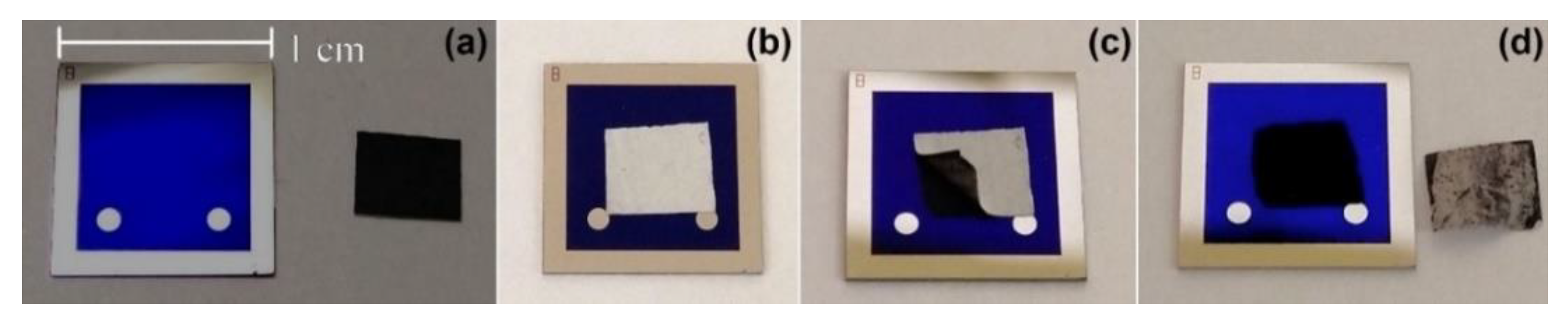
2.1. Device Fabrication

The device was obtained by depositing SWCNTs on a Si3N4/Si substrate using the dry transfer process. The substrate consists of a n-doped silicon wafer (300 µm thickness, 2300–3150 Ωcm resistivity) with the top surface covered by a 60 nm Si3N4 insulating layer. To enable the electrical connection, the back of the substrate was fully covered by a metallic layer (Ti 30 nm/ TiN 50 nm/ Ti 20 nm/ Pt 100 nm), and two similar metallic pads with 1 mm diameter were deposited on top of the substrate. A cross-section of the substrate is reported in Figure 1.
The transfer process consists of two principal phases (Figure 2): The first one is the realization of the SWCNT film and the second one is the transfer of it on to the substrate.
The SWCNT film is obtained by low vacuum filtration of a liquid solution of SWCNTs on a filter membrane. The liquid solution is made of SWCNT powder diluted to 80 µg/mL with distilled water and sodium dodecyl sulphate (SDS, 2% solution weight ratio). The SDS molecules surround the SWCNTs and prevent their aggregation and precipitation in the aqueous medium. The mixture is tip-ultrasonicated for one hour, obtaining a well dispersed compound. After that, the mixture is left for about 10 h to let the bundled nanotubes precipitate. After the removal of this precipitate, a stable mixture that does not show any kind of further SWCNT precipitation, after several months, is obtained. The stable mixture is then deposited on a filter membrane (Durapore PVDF, pore size 0.22 µm, diameter 47 mm) using vacuum filtration and is rinsed with a solution of ethanol, methanol, and water (15%–15%–70%) to remove all the surfactant from the SWCNT film.
The transfer process starts after the SWCNT filter has dried. The transfer is achieved by placing a piece of CNT film over the substrate, by wetting the membrane with water and ethanol, and then by pressing it to improve the adhesion of the film to the substrate. After a few minutes, the dried membrane is peeled off and the CNT film is left over the substrate.

2.2. SWCNT Film Characterization
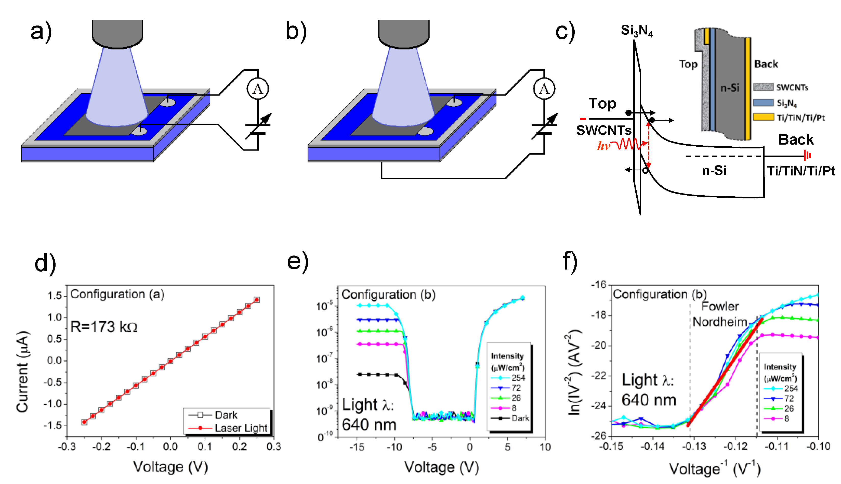
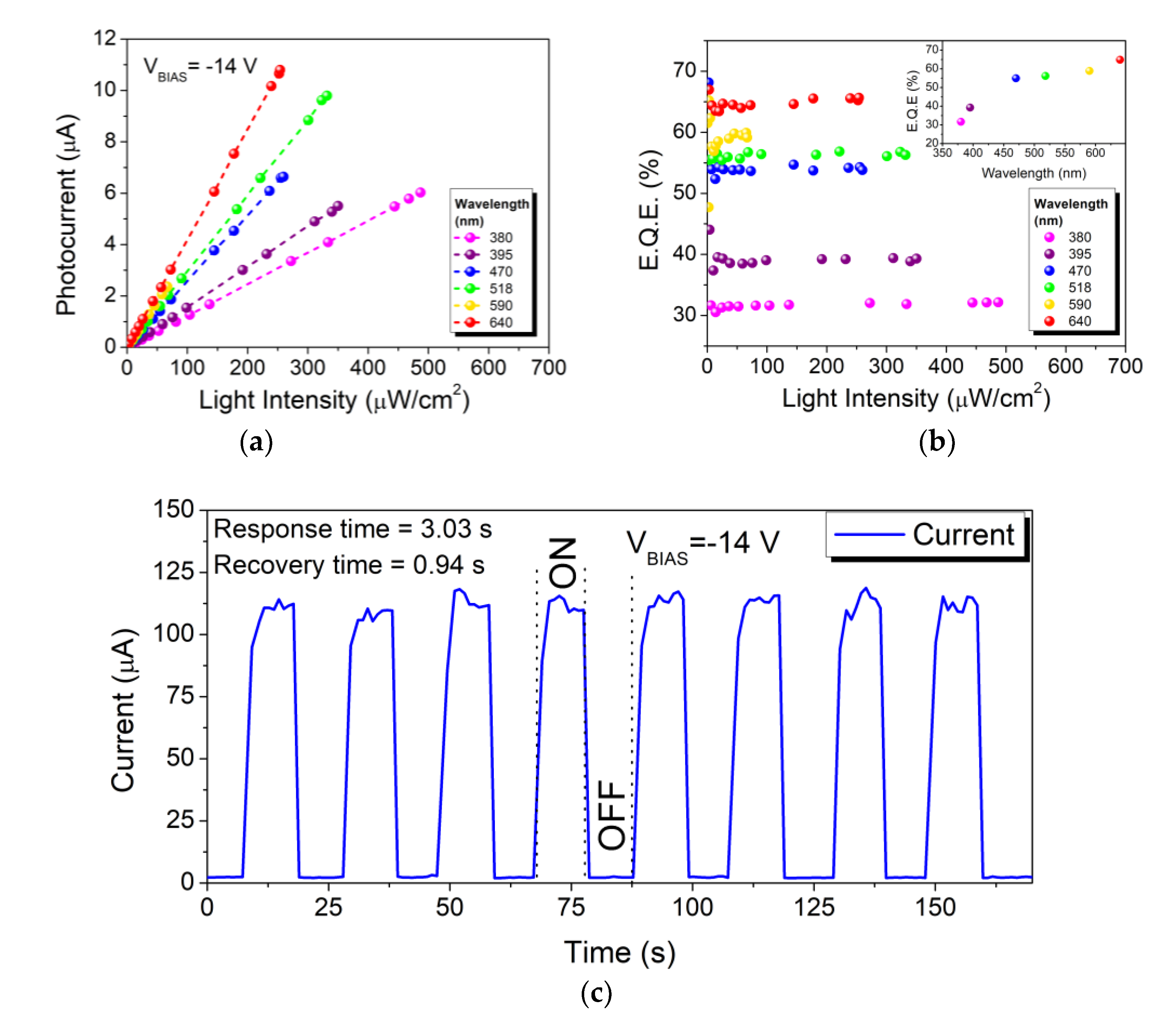
The morphology of the SWCNT film was investigated using a field-emission scanning electron microscope (SEM, Zeiss LEO 1530) at an accelerating voltage of 5 kV. The SWCNTs form a uniform film that covers the substrate surface entirely (Figure 3a). The SWCNTs in the film are randomly oriented and form an intricate three-dimensional net structure (Figure 3b).
The chemical composition of the SWCNT film was investigated by X–ray photoemission spectroscopy (PHI 1257) with Mg Kα radiation. The survey spectrum in Figure 4a shows that the film mainly contains carbon with a small amount of oxygen (due to atmospheric contaminants), nitrogen, and silicon (due to the exposed substrate). Figure 4b shows the deconvoluted XPS spectrum of the core level C 1s. The spectrum has been fitted by the sum of six signals: aromatic rings carbon (C=C/C‒C, 284.8 eV), hydroxyl groups (C–OH, 285.9 eV), epoxy groups (C‒O‒C, 286.9 eV), carbonyl groups (C=O, 288.2 eV), carboxyl groups (C=O(OH), 289.3 eV), and the π-π* shake up (291.1 eV).
Figure 4c shows the valence electron energy loss spectrum (EELS) taken from the SWCNT film. By comparing our spectrum with typical graphite EELS spectra, it is possible to attribute the peak at 5.8 eV to the excitation of the π bound electrons and the broad peak centered at 25.5 eV to the excitation of the (σ+π) bound electrons [22].
To determine the quality of the SWCNT powder, micro–Raman spectra were acquired using a LABRAM spectrometer with a λ = 633 nm (1.96 eV) excitation line. For calibration we used the Raman peak of crystalline silicon. The Raman spectrum of the SWCNT film is reported in Figure 4d, that shows the D and G bands typical of carbon material. The D band, attributed to amorphous carbon, is less intense that the G band, indicating the high quality of the nanotubes. The G band is divided in two peaks: the G+ and G, associated with carbon atom vibration along the axis and along the circumferential direction of the SWCNTs, respectively [23]. In the low frequency region, the radial breathing modes (RBM) typical of SWCNTs are present. Using the following phenomenological relation, it is possible to evaluate the tube diameter d starting from the RBM frequency ω [15]:
d nm = 234 ω cm 1 10
Table 1 summarizes the diameter, the chiral vector index, and the nature of the SWCNT associated to the most intense RBM frequency observed from the Raman spectrum.

3. Results

All electrical and photoresponse measurements were performed with the sample inside a dark box using a source-measure unit Keithley 236 for current-voltage IV characterization. Different LEDs were used as light sources. The light intensity was modulated by neutral filters with different transmittance. An optical fiber was used to direct the light over the device surface. To measure the average photoresponse of the SWCNT-Si3N4-Si heterojunction, the optical fiber was placed at a distance such that the light spot covered most of the deposited SWCNT film. Figure 5a,b shows the setup adopted to measure the IV characteristics of the SWCNT film and the SWCNT–Si3N4–Si structure, in the dark and under illumination.
Initial electrical stress with repeated voltage sweeps in range (−40 V, +7.5 V) was applied to the SWCNT-Si3N4-Si heterojunction until the device showed a high current with reproducible rectifying behavior. The electrical stress causes the local thinning or breakdown of the Si3N4 layer, which is therefore treated as an ultrathin tunneling layer able to withstand a voltage drop and transmit an electrical current [24]. In this situation, a Schottky MIS (metal-insulator-semiconductor) structure is formed at the top surface and an ohmic contact is formed on the back side with the Ti/TiN/Ti/Pt film covering a large area (Figure 5c).
Figure 5d shows the IV characteristic of the SWCNT film in the dark and under illumination by the white light of a supercontinuum laser (SuperK COMPACT by NKT PHOTONICS Blokken 84 DK-3460 Birkerød) in the configuration of Figure 5a. The high conductance of the SWCNT film makes it impossible to detect a photocurrent.
Figure 5e shows the current measured in the configuration of Figure 5b by illuminating the SWCNT film of the device with a 640 nm light source at different intensities. The dark current quickly reaches high values in forward bias, whereas it remains below the noise floor of the experimental setup (around the nanoampere) in reverse bias, until the voltage reaches −7.5 V. At lower voltages, the current exponentially increases for a few orders of magnitude. The exponential growth is due to tunneling trough the MIS barrier, as shown in the band diagram of Figure 5c, which ends up in saturation due to the series resistance [24]. The current around −7.5 V follows the Fowler–Nordheim model, I V d 2 ϕ 1   e x p b d V ϕ 3 2 , that describes tunneling through a triangular barrier under the application of an electric field ( ϕ and d are the height and thickness of the barrier, and b is a constant). This is demonstrated by the linear behavior of the Fowler–Nordheim plot ( l n I / V 2 v s   V 1 ) shown in Figure 5f [25,26]. Moreover, assuming a SWCNT/Si3N4 barrier ϕ = Χ S i 3 N 4 Φ C N T ~ 4.0   eV ( Χ S i 3 N 4 is the electron affinity of Si3N4 [27] and Φ C N T is the work function of the SWCNTs [28]), from the slope of the F–N plot, a Si3N4 thickness less than 7 nm after electric stress can be estimated.
When the device is illuminated, the saturated reverse current shows an increase below −7.5 V (Figure 5e) with steps depending on the incident light intensity. The increase is due to photogeneration in the depletion layer that enhances the current, as shown in Figure 5c. The photocurrent is consistent with the growing photo absorption of Si in the range 380–640 nm. In the range −7.5 to 0 V, a photocurrent is not detected, as it likely occurs below the detection limit of ~ 1 nA of the measurement setup.
Figure 6a shows the photocurrent ( I p h o t o = I l i g h t I d a r k ) calculated as the difference between the current measured when the device is illuminated ( I l i g h t ) and the dark current ( I d a r k ), as a function of the light intensity for different wavelengths. The photocurrent increases towards the red part of the spectrum and is a linear function of the light intensity for all the wavelengths. We point out that the linearity is very important for the practical applications of the proposed photodetector.
We calculated the external quantum efficiency E.Q.E., defined as the percentage of collected electrons over the number of impinging photons:
E . Q . E . % = I p h o t o h c e P λ × 100  
where I p h o t o is the photocurrent, h is the Plank constant, c is the speed of light in vacuum, e is the electron charge, and P and λ are the power and the wavelength of the incident light. The E.Q.E. plot in Figure 6b shows that the efficiency is independent of the light intensity. This is consistent with the linearity of the photocurrent as a function of the light intensity in our device.
We remark that the achieved E.Q.E., up to 65% for red light, is competitive with that observed in other CNT-Si detectors obtained by CVD growth of the CNTs [20] or by other methods [21,29].
Figure 6c shows the current under switching light by the white light of the supercontinuum laser, showing the good stability of the photo response for repeated light on/off cycles and a response and recovery time of few seconds limited by the time constant of the measurement setup [30].
We finally note that the performance of the device could be further optimized by tuning the thickness of the Si3N4 dielectric rather than relying on its thinning/breakdown by electric stress.

4. Conclusions

We have reported the easy fabrication of a SWCNT-Si3N4-Si photo detector that is obtained through the dry transfer of a SWCNT film. The nanotube film acts as a semitransparent charge-collecting layer that allows the light to penetrate inside the substrate. The bias applied to the SWCNT film with respect to the Si substrate allows the separation of the photo charge generated in the Si depletion layer.
We have shown that the SWCNT–Si3N4–Si device has a rectifying behavior and a photocurrent in reverse bias that increases linearly with light intensity.
As photodetectors are used everywhere, the proposed device represents a step forward towards the exploitation of carbon nanotubes in real-life applications.

Author Contributions

Conceptualization, M.P. and A.D.B.; methodology, D.C. and M.P.; software, E.F. and F.G.; validation, L.L., F.G. and M.P.; formal analysis, D.C. and M.P.; investigation, D.C. and E.F.; resources, M.P., L.L. and A.D.B.; data curation, D.C., F.G. and E.F.; writing—original draft preparation, D.C.; writing—review and editing, A.D.B. and M.P.; visualization, L.L., D.C. and F.G.; supervision, A.D.B. and M.P.; project administration, M.P.; funding acquisition, L.L., A.D.B. and M.P. All authors have read and agreed to the published version of the manuscript.

Funding

University of Salerno (grant ORSA218189) and University of L’Aquila. The APC was funded by A.D.B.

Data Availability Statement

The data presented in this study are available on request from the corresponding author.

Conflicts of Interest

The authors declare no conflict of interest.

References

  1. Lamura, G.; Andreone, A.; Yang, Y.; Barbara, P.; Vigolo, B.; Hérold, C.; Marêché, J.-F.; Lagrange, P.; Cazayous, M.; Sacuto, A.; et al. High-Crystalline Single- and Double-Walled Carbon Nanotube Mats Grown by Chemical Vapor Deposition. J. Phys. Chem. C 2007, 111, 15154–15159. [Google Scholar] [CrossRef]
  2. Poudel, Y.R.; Li, W. Synthesis, properties, and applications of carbon nanotubes filled with foreign materials: A review. Mater. Today Phys. 2018, 7, 7–34. [Google Scholar] [CrossRef]
  3. Belin, T.; Epron, F. Characterization methods of carbon nanotubes: A review. Mater. Sci. Eng. B 2005, 119, 105–118. [Google Scholar] [CrossRef]
  4. Bugatti, V.; Viscusi, G.; Di Bartolomeo, A.; Iemmo, L.; Zampino, D.C.; Vittoria, V.; Gorrasi, G. Ionic Liquid as Dispersing Agent of LDH-Carbon Nanotubes into a Biodegradable Vinyl Alcohol Polymer. Polymers 2020, 12. [Google Scholar] [CrossRef] [PubMed] [Green Version]
  5. Guadagno, L.; De Vivo, B.; Di Bartolomeo, A.; Lamberti, P.; Sorrentino, A.; Tucci, V.; Vertuccio, L.; Vittoria, V. Effect of functionalization on the thermo-mechanical and electrical behavior of multi-wall carbon nanotube/epoxy composites. Carbon N. Y. 2011, 49, 1919–1930. [Google Scholar] [CrossRef]
  6. Gorrasi, G.; Bugatti, V.; Milone, C.; Mastronardo, E.; Piperopoulos, E.; Iemmo, L.; Di Bartolomeo, A. Effect of temperature and morphology on the electrical properties of PET/conductive nanofillers composites. Compos. Part B Eng. 2018, 135, 149–154. [Google Scholar] [CrossRef]
  7. Gorrasi, G.; Sarno, M.; Di Bartolomeo, A.; Sannino, D.; Ciambelli, P.; Vittoria, V. Incorporation of carbon nanotubes into polyethylene by high energy ball milling: Morphology and physical properties. J. Polym. Sci. Part B Polym. Phys. 2007, 45, 597–606. [Google Scholar] [CrossRef]
  8. Kruss, S.; Hilmer, A.J.; Zhang, J.; Reuel, N.F.; Mu, B.; Strano, M.S. Carbon nanotubes as optical biomedical sensors. Adv. Drug Deliv. Rev. 2013, 65, 1933–1950. [Google Scholar] [CrossRef]
  9. Zaporotskova, I.V.; Boroznina, N.; Parkhomenko, Y.N.; Kozhitov, L.V. Carbon nanotubes: Sensor properties. A review. Mod. Electron. Mater. 2016, 2, 95–105. [Google Scholar] [CrossRef]
  10. Giordano, C.; Filatrella, G.; Sarno, M.; Di Bartolomeo, A. Multi-walled carbon nanotube films for the measurement of the alcoholic concentration. Micro Nano Lett. 2019, 14, 304–308. [Google Scholar] [CrossRef] [Green Version]
  11. Dekker, C. How we made the carbon nanotube transistor. Nat. Electron. 2018, 1, 518. [Google Scholar] [CrossRef]
  12. Hu, X.; Hou, P.; Liu, C.; Cheng, H. Carbon nanotube/silicon heterojunctions for photovoltaic applications. Nano Mater. Sci. 2019, 1, 156–172. [Google Scholar] [CrossRef]
  13. Coscia, U.; Ambrosone, G.; Ambrosio, A.; Ambrosio, M.; Bussolotti, F.; Carillo, V.; Grossi, V.; Maddalena, P.; Passacantando, M.; Perillo, E.; et al. Photoconductivity of multiwalled CNT deposited by CVD. Solid State Sci. 2009, 11, 1806–1809. [Google Scholar] [CrossRef]
  14. Melisi, D.; Nitti, M.A.; Valentini, M.; Valentini, A.; Ligonzo, T.; De Pascali, G.; Ambrico, M. Photodetectors based on carbon nanotubes deposited by using a spray technique on semi-insulating gallium arsenide. Beilstein J. Nanotechnol. 2014, 5, 1999–2006. [Google Scholar] [CrossRef] [Green Version]
  15. Passacantando, M.; Grossi, V.; Santucci, S. High photocurrent from planar strips of vertical and horizontal aligned multi wall carbon nanotubes. Appl. Phys. Lett. 2012, 100, 163119. [Google Scholar] [CrossRef]
  16. Passacantando, M.; Bussolotti, F.; Grossi, V.; Santucci, S.; Ambrosio, A.; Ambrosio, M.; Ambrosone, G.; Carillo, V.; Coscia, U.; Maddalena, P.; et al. Photoconductivity in defective carbon nanotube sheets under ultraviolet–visible–near infrared radiation. Appl. Phys. Lett. 2008, 93, 51911. [Google Scholar] [CrossRef] [Green Version]
  17. Tinti, A.; Righetti, F.; Ligonzo, T.; Valentini, A.; Nappi, E.; Ambrosio, A.; Ambrosio, M.; Aramo, C.; Maddalena, P.; Castrucci, P.; et al. Electrical analysis of carbon nanostructures/silicon heterojunctions designed for radiation detection. Nucl. Instrum. Methods Phys. Res. Sect. A Accel. Spectrometers Detect. Assoc. Equip. 2011, 629, 377–381. [Google Scholar] [CrossRef]
  18. 1Wu, D.; Guo, J.; Wang, C.; Ren, X.; Chen, Y.; Lin, P.; Zeng, L.; Shi, Z.; Li, X.J.; Shan, C.-X.; et al. Ultrabroadband and High-Detectivity Photodetector Based on WS2/Ge Heterojunction through Defect Engineering and Interface Passivation. ACS Nano 2021, 15, 10119–10129. [Google Scholar] [CrossRef]
  19. De Nicola, F.; Castrucci, P.; Scarselli, M.; Nanni, F.; Cacciotti, I.; De Crescenzi, M. Multi-Fractal Hierarchy of Single-Walled Carbon Nanotube Hydrophobic Coatings. Sci. Rep. 2015, 5, 8583. [Google Scholar] [CrossRef] [Green Version]
  20. Aramo, C.; Ambrosio, M.; Bonavolontà, C.; Boscardin, M.; Crivellari, M.; de Lisio, C.; Grossi, V.; Maddalena, P.; Passacantando, M.; Valentino, M. Large area CNT-Si heterojunction for photodetection. Nucl. Instrum. Methods Phys. Res. Sect. A Accel. Spectrometers Detect. Assoc. Equip. 2017, 845, 12–15. [Google Scholar] [CrossRef]
  21. Ismail, R.A.; Mohammed, M.I.; Mahmood, L.H. Preparation of multi-walled carbon nanotubes/n-Si heterojunction photodetector by arc discharge technique. Optik 2018, 164, 395–401. [Google Scholar] [CrossRef]
  22. Camilli, L.; Pisani, C.; Gautron, E.; Scarselli, M.; Castrucci, P.; D’Orazio, F.; Passacantando, M.; Moscone, D.; De Crescenzi, M. A three-dimensional carbon nanotube network for water treatment. Nanotechnology 2014, 25, 065701. [Google Scholar] [CrossRef] [PubMed]
  23. Dresselhaus, M.S.; Dresselhaus, G.; Saito, R.; Jorio, A. Raman spectroscopy of carbon nanotubes. Phys. Rep. 2005, 409, 47–99. [Google Scholar] [CrossRef]
  24. Di Bartolomeo, A.; Giubileo, F.; Grillo, A.; Luongo, G.; Iemmo, L.; Urban, F.; Lozzi, L.; Capista, D.; Nardone, M.; Passacantando, M. Bias Tunable Photocurrent in Metal-Insulator-Semiconductor Heterostructures with Photoresponse Enhanced by Carbon Nanotubes. Nanomaterials 2019, 9, 1598. [Google Scholar] [CrossRef] [PubMed] [Green Version]
  25. Di Bartolomeo, A.; Scarfato, A.; Giubileo, F.; Bobba, F.; Biasiucci, M.; Cucolo, A.M.; Santucci, S.; Passacantando, M. A local field emission study of partially aligned carbon-nanotubes by atomic force microscope probe. Carbon 2007, 45, 2957–2971. [Google Scholar] [CrossRef] [Green Version]
  26. Di Bartolomeo, A.; Rücker, H.; Schley, P.; Fox, A.; Lischke, S.; Na, K.Y. A single-poly EEPROM cell for embedded memory applications. Solid-State Electron. 2009, 53, 644–648. [Google Scholar] [CrossRef]
  27. Tao, S.X.; Theulings, A.; Smedley, J.; van der Graaf, H. DFT study of electron affinity of hydrogen terminated β-Si3N4. Diamond Related Mater. 2015, 53, 52–57. [Google Scholar] [CrossRef]
  28. Liu, P.; Sun, Q.; Zhu, F.; Liu, K.; Jiang, K.; Liu, L.; Li, Q.; Fan, S. Measuring the Work Function of Carbon Nanotubes with Thermionic Method. Nano Lett. 2008, 8, 2, 647–651. [Google Scholar] [CrossRef]
  29. Salvato, M.; Scagliotti, M.; De Crescenzi, M.; Boscardin, M.; Attanasio, C.; Avallone, G.; Cirillo, C.; Prosposito, P.; De Matteis, F.; Messi, R.; et al. Time response in carbon nanotube/Si based photodetectors. Sens. Actuators A 2019, 292, 71–76. [Google Scholar] [CrossRef]
  30. Liao, M. Progress in semiconductor diamond photodetectors and MEMS sensors. Funct. Diam. 2021, 1, 29–46. [Google Scholar] [CrossRef]
Figure 1. Schematic representation of the substrate cross-section.
Electronics 11 00271 g001
Figure 2. Phases of the dry transfer process. (a) Substrate and piece of SWCNT filter before the transfer. (b) SWCNT film pressed over the substrate surface after wetting it with water and ethanol. It is important to place the film in contact with the metallic pads to facilitate the connection of the device with the measurement equipment. (c) Peel-off of the membrane. (d) Detector with deposited SWCNT film and membrane after the transfer process.
Electronics 11 00271 g002
Figure 3. (a) SEM image at low magnification of the SWCNT film. The nanotubes cover the substrate surface entirely; it is possible to see some residues of the membrane used for the transfer process. (b) SEM image at high magnification of the SWCNT film.
Electronics 11 00271 g003
Figure 4. (a) Survey spectra of SWCNT film revealing the presence of oxygen and nitrogen due to the adsorption of atmospheric contaminants. (b) C 1s spectra. (c) Energy loss spectra. (d) Raman spectra.
Electronics 11 00271 g004
Figure 5. (a) Pad to pad horizontal measurement configuration and (b) top–back vertical measurement configuration. (c) Band diagram of the device in reverse bias showing tunneling through the top barrier and photogeneration in the top depletion layer (the back contact is ohmic). The cross section of the device is also shown. (d) IV characteristics of the SWCNT film (configuration a) in the dark and under illumination by a white light (wavelength in the range 450 nm to 2400 nm and intensity 2   W / cm 2 ). (e) IV curves of SWCNT−Si3N4−Si MIS structure in configuration b) (top-back) under 640 nm light at different light intensities. (f) Fowler–Nordheim plot of the IV curves of the SWCNT−Si3N4−Si MIS structure around V = −7.5 V (the red straight-line Y = a + b   X = 26 + 392   X is the fit of 26 μ W / cm 2 data–green curve).
Electronics 11 00271 g005
Figure 6. (a) Photocurrent vs. light intensity in reverse bias (V = −14 V) for different wavelengths. (b) Calculated E.Q.E. as a function of the light intensity for different wavelengths and (inset) average external quantum efficiency, E.Q.E., as a function of the wavelength. (c) Device current under switching white light (wavelength in the range 450 nm to 2400 nm and intensity 2   W / cm 2 ).
Electronics 11 00271 g006
Table 1. RBM frequency (ω) obtained from the Raman spectrum and the evaluated diameter (d), chiral vector index (n,m), and nature of the SWCNTs.
ω (cm−1)d (nm)(n,m)Type
267.20.91(8,5)Metallic
294.30.82(9,2)Semiconductor
Publisher’s Note: MDPI stays neutral with regard to jurisdictional claims in published maps and institutional affiliations.

