Article

Investigation of AlGaN Channel HEMTs on β-Ga2O3 Substrate for High-Power Electronics

by
A. Revathy
1,*,
C. S. Boopathi
1,*,
Osamah Ibrahim Khalaf
2 and
Carlos Andrés Tavera Romero
3
1
Department of Electrical and Electronics Engineering, SRM Institute of Science and Technology, Chennai 603203, India
2
Al-Nahrain Nano Renewable Energy Research Center, Al-Nahrain University, Baghdad 10072, Iraq
3
COMBA R&D Laboratory, Faculty of Engineering, Universidad Santiago de Cali, Cali 76001, Colombia
*
Authors to whom correspondence should be addressed.
Electronics 2022, 11(2), 225; https://doi.org/10.3390/electronics11020225
Submission received: 25 November 2021 / Revised: 30 December 2021 / Accepted: 6 January 2022 / Published: 12 January 2022
(This article belongs to the Topic Application of Innovative Power Electronic Technologies)

Abstract

:
The wider bandgap AlGaN (Eg > 3.4 eV) channel-based high electron mobility transistors (HEMTs) are more effective for high voltage operation. High critical electric field and high saturation velocity are the major advantages of AlGaN channel HEMTs, which push the power electronics to a greater operating regime. In this article, we present the DC characteristics of 0.8 µm gate length (LG) and 1 µm gate-drain distance (LGD) AlGaN channel-based high electron mobility transistors (HEMTs) on ultra-wide bandgap β-Ga2O3 Substrate. The β-Ga2O3 substrate is cost-effective, available in large wafer size and has low lattice mismatch (0 to 2.4%) with AlGaN alloys compared to conventional SiC and Si substrates. A physics-based numerical simulation was performed to investigate the DC characteristics of the HEMTs. The proposed HEMT exhibits sheet charge density (ns) of 1.05 × 1013 cm−2, a peak on-state drain current (IDS) of 1.35 A/mm, DC transconductance (gm) of 277 mS/mm. The ultra-wide bandgap AlGaN channel HEMT on β-Ga2O3 substrate with conventional rectangular gate structure showed 244 V off-state breakdown voltage (VBR) and field plate gate device showed 350 V. The AlGaN channel HEMTs on β-Ga2O3 substrate showed an excellent performance in ION/IOFF and VBR. The high performance of the proposed HEMTs on β-Ga2O3 substrate is suitable for future portable power converters, automotive, and avionics applications.

1. Introduction

Group III-nitride-based heterostructure devices showed excellent performance in high-power switching electronics [1,2,3]. Owing to the unique material properties of GaN such as high breakdown field (3.3 MV/cm), high mobility (>1200 cm2/v.s), and wide bandgap (3.4 eV), the GaN-based high electron mobility transistors (HEMTs) are exhibited high 2DEG density (two-dimensional electron gas), low on-resistance (Ron), low conduction loss, and high breakdown voltage (VBR). Which enable the devices for high-temperature and high-power switching applications [4,5]. However, it is difficult to obtain high breakdown voltage for GaN-channel based HEMTs for smaller dimensions for portable high power switching applications like power converters, automotive electronics, and avionics. Therefore, further enhancing the power handling capability of the HEMTs, the ultra-wide bandgap (>3.4 eV) AlxGa1−xN channel-based devices are widely used [6,7,8,9,10,11]. There is a wide bandgap and superior thermal stability in AlGaN material adopted as a channel for improving the high-power handling and high-temperature operations of HEMTs. Gate length 2 µm (LG) AlN/Al0.5Ga0.5N HEMT on sapphire substrate demonstrated remarkable breakdown voltage improvements [6]. LG = 0.8 µm and LGD = 1 µm Al0.31Ga0.69N/Al0.1Ga0.9N double-channel HEMTs recorded a VBR of 143.5 V [8]. However, the device has shown a large negative threshold voltage (VTH = −11.2 V), which will increase the power loss of the device at off-state. An Al-rich AlN/Al0.85Ga0.15N HEMTs on sapphire substrate showed 810 V of breakdown voltage (VBR) for a gate-drain distance of (LGD) of 10 µm [9]. Another Al-rich AlN/Al0.65Ga0.35N HEMTs on the sapphire substrate demonstrated 770 V off-state blocking voltage for 9 µm LGD [10]. LG = 3 µm Al0.3Ga0.7N/Al0.1Ga0.9N heterostructure on sapphire substrate exhibited excellent sheet carrier density and electron mobility [11], and hybrid ohmic/Schottky drain device configuration showed excellent off-state breakdown voltage. Despite high off-state blocking voltage of Al-rich AlGaN channel HEMTs [6,9,10], the current driving capability is very low due to alloy disorder scattering effects. On other hand, low Al composition AlGaN channel-based HEMTs [8,11] exhibited excellent sheet charge density and carrier mobility.
Apart from channel engineering, substrate engineering is one of the key issues in group III-nitride-based HEMTs. Sapphire (13% lattice mismatch with GaN), SiC (3.8% lattice mismatch with GaN), and Si (16% lattice mismatch with GaN) are widely used as substrate materials for GaN-based HEMTs [1,2,3,4,5,6,7,8,9,10,11]. Due to lattice mismatch between buffer and substrate materials, an additional AlN layer is required in between for lattice match, which involves additional costs and increases the device fabrication complexity.
Recently, β-Ga2O3 is an emerging material for power electronics applications. The wide bandgap (4.7 eV), high critical electric field (6–8 MV/cm), large-scale, high-quality bulk substrate, low defect density, and nearly lattice match (0 to 2.4% lattice mismatch for AlGaN alloys) with III-Nitride alloys make β-Ga2O3 a promising material for future high-power applications [12,13,14,15,16,17,18]. A numerical study on normally-off AlN/β-Ga2O3 based HEMT with GaN back barrier showed a suppressed leakage current and excellent DC characteristics [19]. In spite of high-power performance, the β-Ga2O3 channel-based HEMTs experienced low electron mobility and low sheet charge concentration [18] as a result of low current driving capability. In this work, we used β-Ga2O3 as a substrate for the following reasons. 1. Low lattice mismatch with AlGaN alloys and therefore an additional thick AlN nucleation layer is not required 2. Relatively low cost compared to GaN and SiC, and 3. Availability of large wafer size. The novelty of the work is gate field plate AlGaN channel HEMTs on β-Ga2O3 substrate.
The first Al0.1Ga0.9N channel-based HEMTs on the β-Ga2O3 substrate is proposed in this work for simultaneous improvement in both power handling and current driving capability of HEMTs. The proposed gate field plate Al0.31Ga0.69N/Al0.1Ga0.9N HEMTs on β-Ga2O3 substrate is investigated using ATLAS TCAD [20] and the device DC characteristics are presented. The device simulation models are validated with the experimental results. The field plate gate low Al composition (Al = 10%) AlGaN channel HEMT on β-Ga2O3 substrate showed remarkable improvement in breakdown voltage (VBR), on-state drain current density, and low on-resistance.

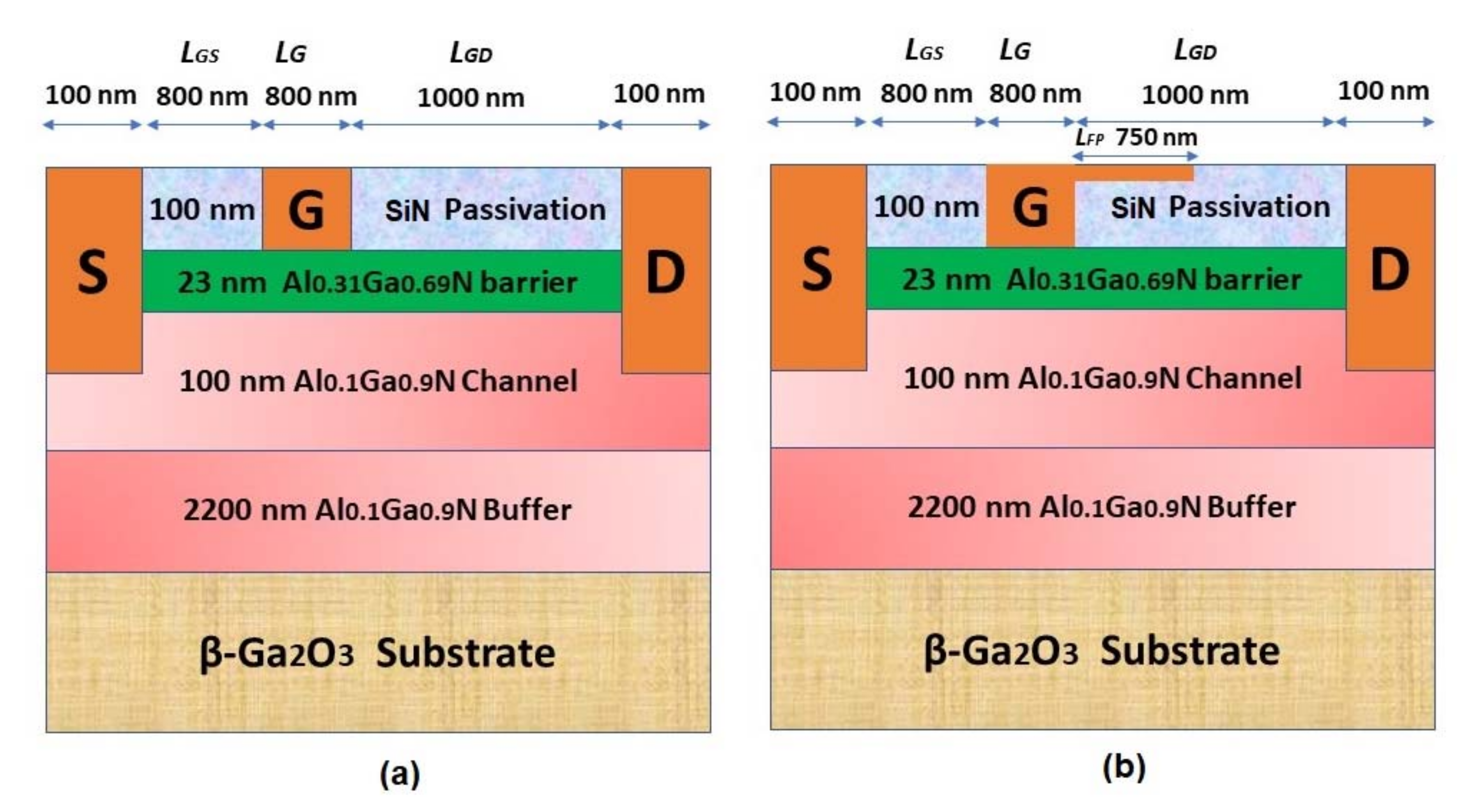
2. Device Structure and Simulation Model

Figure 1a shows the schematic cross-section of the conventional gate Al0.1Ga0.9N channel HEMT (Device A) on β-Ga2O3 substrate and field plate gate HEMT (Device B) is displayed in Figure 1b. Both device’s epi-stack consist of 100 nm Al0.1Ga0.9N channel, 23 nm Al0.31Ga0.69N barrier, and 2.2 µm Al0.31Ga0.69N buffer, 100 nm SiN passivation (Ɛr~7). Low Al-composition Al0.1Ga0.9N channel is used in this to improve the sheet charge density (2DEG) and enhance electron mobility (µ) [8,11]. The Al0.1Ga0.9N layer is directly grown on the β-Ga2O3 substrate. A low lattice mismatch (<2.4%) between AlGaN buffer and β-Ga2O3 substrate alleviates the interface defects and enhanced the device performance. Moreover, the β-Ga2O3 wafer is available in a larger size and low cost compared with SiC and GaN [12,13,14,15,16,17,18]. Device gate length is defined as 0.8 µm (LG) and asymmetrical gate to source (LGS = 0.8 µm) and gate to drain distance (LGD = 1 µm) is considered for this work in order to reduce the source resistance. To analyze the impact of filed plate structure on the breakdown performance of the AlGaN channel HEMT, a 0.75 µm field plate (LFP) was used in Device B. Ohmic contact was realized for source and drain contact by defining the work function of the electrode as 3.4 eV and Schottky gate contact enabled by defining electrode work function as 5.2 eV. Field plate gate structure used for the proposed HEMT for improving the off-state blocking voltage of the device by re-shaping the electric field across the gate to the drain access region. The SiN passivation avoids the surface-related trapping effects and avoids the current collapse phenomena.
The TCAD simulation energy band diagram is plotted in Figure 2 at zero gate bias and drain bias. It shows the conduction band discontinuity at the interface of Al0.31Ga0.69N/Al0.1Ga0.9N and forms a 2DEG due to spontaneous and piezoelectric polarization effects. The sheet charge density (ns) of 1.05 × 1013 cm−2 extracted from the device simulation. The corresponding polarization charge details are displayed in Figure 3. The material parameters for the simulation are taken from [16,17,18,19,20,21,22] and are presented in Table 1.
The basic device physics models that operate on any semiconductor devices have been derived from Schrodinger’s equation, Shockley–Read–Hall (SRH) recombination model, Poisson’s equations, the continuity equations, and the transport equations. The quantum electron density relies on the one-dimensional (1D) Schrodinger’s equation, which relates the eigen state energies E i v x and wave function φ i v x , y .
h 2 2 y 1 m y v x , y φ i v y + E C x , y φ i v = E i v φ i v
where m y v x , y indicates spatial dependent effective mass and E C x , y represents the conduction band edge. Poisson’s equations relate the electric field (E), electrostatic potential ( ψ ), and space charge concentration ( ρ ). Which is written as follows [20];
2 ψ = E = ρ ε
The continuity and transport equations describe the time-dependent electron (n) and hole (p) densities due to carrier transport, carrier generation ( G n and G p ), and carrier recombination ( R n and R p ) process. The continuity equations are defined by the following equations [20];
n t = 1 q J n + G n R n
p t = 1 q J p + G p R p
The drift-diffusion carrier transport model is based on Boltzmann transport theory, which relates the current densities ( J n and J p ) with quasi-Fermi levels ( n and p ) and the quasi-Fermi levels are related with carrier concentrations and potentials through Boltzmann approximations [20].
J n = q μ n n n
J p = q μ p p p
The polarization property of group III-nitride is the major source for 2DEG, the spontaneous (PSP) and piezoelectric polarization (PPZ) models are used for the device simulation. The carrier mobility impacts the device on-state current density (IDS) and transconductance (gm). Therefore, the temperature, composition, and doping dependent Farahmand Modified Caughey Thomas low field mobility model (FMCT.N) and nitride specific high field mobility (GANSAT.N) models [20] are used in this work. In order to capture the trap-assisted recombination due to crystal defects and dopant, Shockley–Read–Hall (SRH) recombination model is used for the device simulation. Which is described by the following equations [20];
R n e t S R H = n n i e 2 τ p p + n i e exp E t r a p K T + τ n p + n i e exp E t r a p K T
where τ p and τ n are electron and hole lifetime, respectively, and E t r a p defines the intrinsic Fermi energy level to trap energy level. The impact ionization model described by Selberherr used for device breakdown simulation, which relates the carrier generation ( G ) rate with electron ( α n ) and hole ionization coefficients ( α p ), and electron ( J n ) and hole current densities ( J p ) [20];
G = α p J p + α n J n

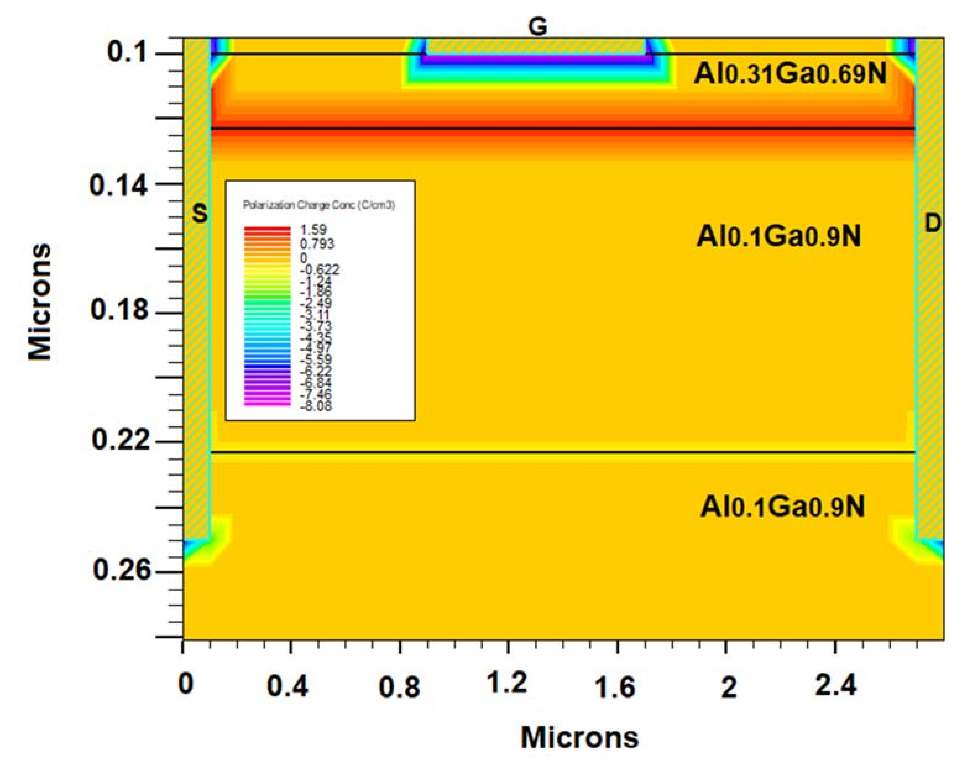
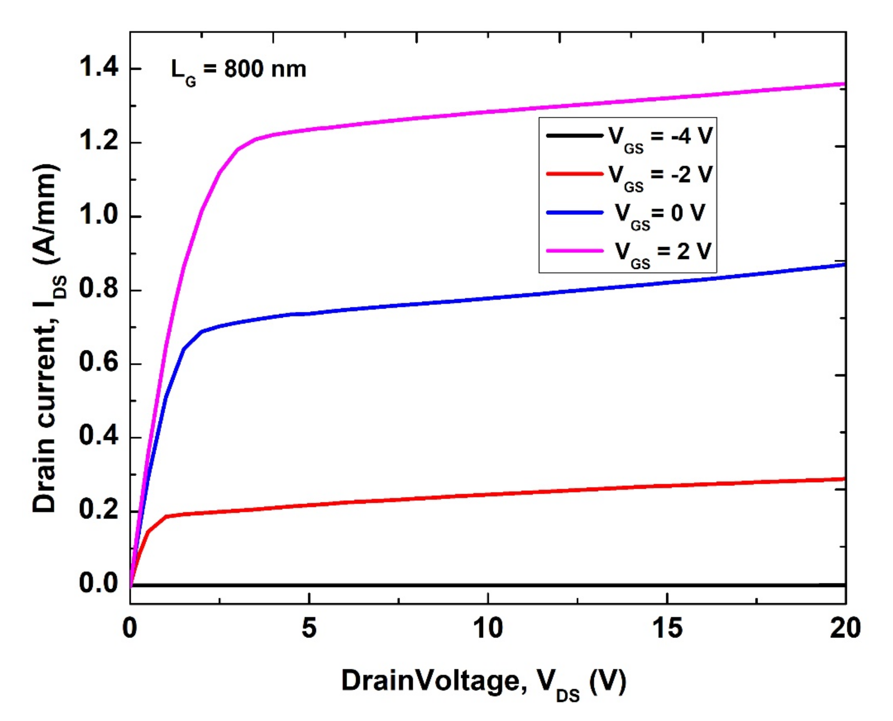
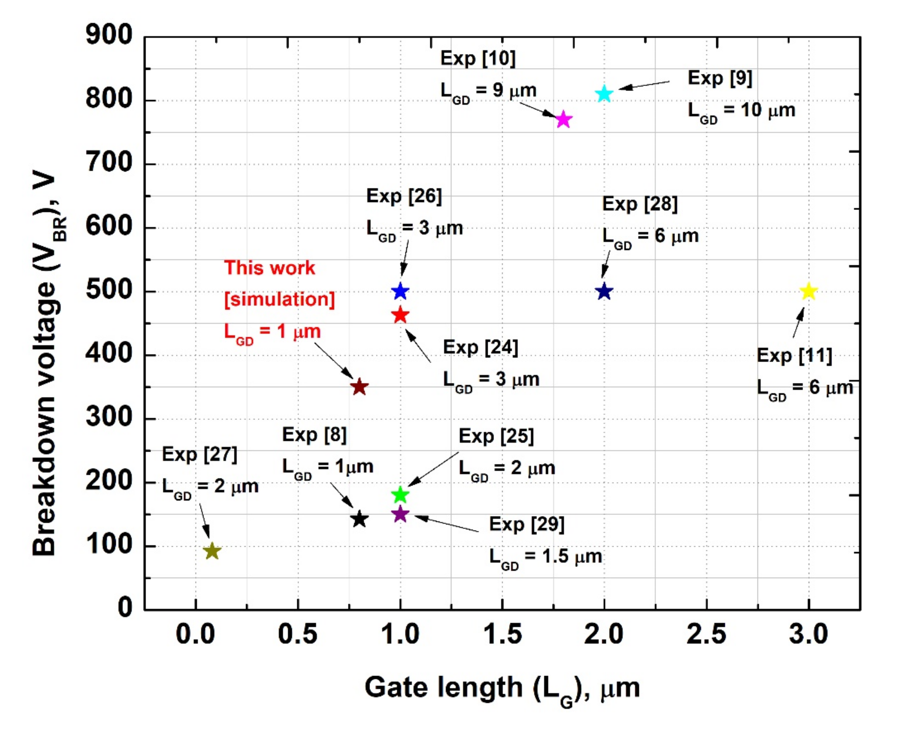
3. Results and Discussions

The current driving ( J = q v n s ) capability of the HEMTs relies on the electron velocity ( v ), sheet charge, and 2DEG density (ns). The proposed HEMT showed 1.12 × 107 cm/s of electron velocity and sheet charge density (ns) of 1.05 × 1013 cm−2. The DC characteristics of proposed AlGaN channel HEMTs on β-Ga2O3 are presented in this section. The device output characteristics is plotted in Figure 4 for VGS = −4 V to 8 V and VDS from 0 V to 20 V. The HEMT showed a peak on-state drain current (IDS) of 1.35 A/mm at VGS = 2 V and the extracted ON-resistance (RON = ∆VDS/∆IDS) from the V-I curve corresponding to VGS = 0 V is 8.83 Ω.mm. The DC transfer characteristics of HEMT is displayed in Figure 5a at VDS = 10 V and VGS swept from −10 V to 8 V. A peak transconductance (gm) of 277 mS/mm obtained at VGS = −1.5 V and extracted a threshold voltage of −4.31 V. The device transfer characteristics log-scale plot displayed in Figure 5b and the HEMT showed an excellent ION/IOFF ratio of ~1014. The obtained IDS and gm are the highest results among the AlxGa1−xN channel HEMTs [6,7,8,9,10,11]. The TCAD simulation is validated with the LG = 0.8 µm gate length AlGaN channel HEMT experimental results for transfer and breakdown performance [8] and depicted in Figure 6, which shows the simulation results are well correlated with experimental results.
For power electronics applications, low ON-resistance (RON) and high breakdown voltage (VBR) are the most critical parameters to minimize the resistive losses during high power operation of HEMTs, which determine the efficiency of the power devices. In III-nitride-based HEMTs, the 2DEG is induced by polarization, and the breakdown voltage depends on the gate-to-drain distance (LGD). The ON-resistance of the HEMT expressed as following expressions [23];
R o n = R c h a n n e l + R d r a i n = L G W G · 1 q μ n s + L G D W G · 1 q μ n s
where R c h a n n e l is the channel resistance and R d r a i n is drain side access resistance. Primarily, the off-state breakdown voltage depends on L G D = V B R E c r i t when source and drain contact resistances are neglected. In general, longer gate length and larger gate-drain spacing HEMTs typically exhibit high VBR but the ON-resistance also increased with L G [23]. Shorter gate length and small L G D HEMTs showed low breakdown voltages. Hence, the optimization of HEMTs structure is the key component for achieving high breakdown field and low RON for future low loss power semiconductor devices with smaller device sizes. In this work, we used LG = 800 nm gate length and LGD = 1000 nm ultra-wide bandgap AlGaN channel along with gate field structure. In addition, the obtained results were compared with existing HEMTs with same LG and LGD [8].
The high critical electric field of AlGaN channel (~4×) HEMTs to GaN-channel HEMTs leads to high voltage operation of the device. Figure 7 shows the forward blocking characteristics of the conventional AlGaN channel and gate field plate AlGaN channel HEMTs. The off-state breakdown voltage (VBR) is extracted from VD-ID when drain leakage current reaches 1 mA/mm. As shown in Figure 7, LG = 0.8 µm conventional AlGaN channel HEMT on β-Ga2O3 substrate demonstrated 244 V of VBR and LG = 0.8 µm and LFP = 0.75 µm gate field plate HEMT on β-Ga2O3 substrate showed a VBR of 350 V. The field plate HEMT modulates the electric field in the device access regions (gate-drain space) and able to sustain high electric fields, which leads to enhanced breakdown voltage. Logarithmic electron concentration of the HEMTs is displayed in Figure 8 at the breakdown condition. The Depletion region of gate field plate HEMT in Figure 8b is larger than the conventional gate HEMT Figure 8a. This represents that the higher depletion width leads to high VBR and the smaller depletion width would decrease the VBR of the HEMT. Gate field plate AlGaN channel HEMT on β-Ga2O3 substrate exhibited excellent breakdown characteristics and low ON-resistance than existing AlGaN channel HEMT with identical device size [8]. This reveals the potential of AlGaN channel HEMTs on β-Ga2O3 substrate for future power switching applications with smaller device sizes. The comparison of proposed AlGaN channel HEMTs breakdown performance with previously reported AlGaN channel HEMTs [8,9,10,11,24,25,26,27,28,29] are presented in Figure 9. Our device showed excellent breakdown voltage than existing HEMTs for smaller gate length (LG) and gate-drain distance (LGD).
The tentative fabrication steps of the proposed HEMT are depicted in Figure 10. The epitaxial growth can be performed by the MOCVD process (Metal Organic Chemical Vapor Deposition) on the β-Ga2O3 substrate. Device mesa isolation will reduce the reducing leakage currents. This can be achieved through dry etching ICP-RIE (Inductively Coupled Plasma Reactive Ion Etching). The patterned deposition of source and drain contacts will be conducted through optical lithography and e-beam evaporation followed by high-temperature annealing. The minimum feature size used is 1 micron hence patterning is possible through optical lithography for lower feature sizes one has to depend on e-beam lithography. Then, patterning and deposition of gate metal followed by contact annealing at a lower temperature to ensure Schottky nature of the contact. Blanket deposition of silicon nitride through PECVD (Plasma Enhanced Chemical Vapor Deposition) and ALD (Atomic Layer Deposition) over the entire substrate. Selective etching of SiN for source, gate, and drain pad openings through ICP-RIE.

4. Conclusions

AlGaN channel HEMTs on β-Ga2O3 substrate are proposed and the device DC characteristics with rectangular and gate field plate structures are analyzed. The wide-bandgap AlGaN channel along with field plate gate HEMT showed improved breakdown voltage (VBR) of 350 V for LG = 0.8 µm and LGD = 1 µm, whereas the conventional gate HEMT with identical device dimensions showed 244 V of VBR. The improved breakdown voltage from the larger depletion region at breakdown condition in field plate HEMT. The low Al composition Al0.1Ga0.9N channel also demonstrated a peak ON-state current density of 1.35 A/mm, 8.83 Ω.mm of RON, and gm of 277 mS/mm. TCAD simulation and DC characteristics of the β-Ga2O3 substrate-based AlGaN channel HEMTs indicates the suitability of proposed HEMTs for future portable less weight power converters, motor driver, consumer electronics, automotive, and avionics applications. In addition, the β-Ga2O3 substrate can be utilized for all group III-nitride-based transistors for better performance.

Author Contributions

Conceptualization, methodology, software, validation, A.R.; formal analysis, investigation, resources, data curation, writing—original draft preparation, supervision, C.S.B.; writing—review and editing, visualization, O.I.K.; project administration, funding acquisition, C.A.T.R. All authors have read and agreed to the published version of the manuscript.

Funding

This research has been funded by Dirección General de Investigaciones of Universidad Santiago de Cali under call No. 01-2021.

Institutional Review Board Statement

Not applicable.

Informed Consent Statement

Not applicable.

Data Availability Statement

The data presented in this study will be provided based on reasonable request to corresponding authors.

Acknowledgments

The authors would like to thank to the SRM Institute of Science and Technology, Chennai and Universidad Santiago de Cali for providing necessary support to carry out the research work.

Conflicts of Interest

The authors declare no conflict of interest.

References

  1. Ma, C.T.; Gu, Z.H. Review of GaN HEMT Applications in Power Converters over 500 W. Electronics 2019, 8, 1401. [Google Scholar] [CrossRef] [Green Version]
  2. Koksaldi, O.S.; Haller, J.; Li, H.; Romanczyk, B.; Guidry, M.; Wienecke, S.; Keller, S.; Mishra, U.K. N-Polar GaN HEMTs Exhibiting Record Breakdown Voltage Over 2000 V and Low Dynamic On-Resistance. IEEE Electron Device Lett. 2018, 39, 1014–1017. [Google Scholar] [CrossRef]
  3. Huang, X.; Liu, Z.; Li, Q.; Lee, F.C. Maximizing the performance of 650-V p-GaN gate HEMTs: Dynamic RON characterization and circuit design considerations. IEEE Trans. Power Electron. 2017, 32, 5539–5549. [Google Scholar]
  4. Lidow, A.; Strydom, J.; de Rooij, M.; Reusch, D. GaN Transistors for Efficient Power Conversion; Willey: New York, NY, USA, 2015. [Google Scholar]
  5. Meneghini, M.; Gaudenzio, M.; Zanoni, E. Power GaN Devices—Materials, Applications and Reliability; Springer: New York, NY, USA, 2017. [Google Scholar]
  6. Abid, I.; Mehta, J.; Cordier, Y.; Derluyn, J.; Degroote, S.; Miyake, H.; Medjdoub, F. AlGaN Channel High Electron Mobility Transistors with Regrown Ohmic Contacts. Electronics 2021, 10, 635. [Google Scholar] [CrossRef]
  7. Kaplar, R.J.; Allerman, A.A.; Armstrong, A.M.; Crawford, M.H.; Dickerson, J.R.; Fischer, A.J.; Baca, A.G.; Douglas, E.A. Review—Ultra-Wide-Bandgap AlGaN Power Electronic Devices. ECS J. Solid State Sci. Technol. 2017, 6, Q3061–Q3066. [Google Scholar] [CrossRef]
  8. Zhang, Y.; Li, Y.; Wang, J.; Shen, Y.; Du, L.; Li, Y.; Wang, Z.; Xu, S.; Zhang, J.; Hao, Y. High-Performance AlGaN Double Channel HEMTs with Improved Drain Current Density and High Breakdown Voltage. Nanoscale Res. Lett. 2020, 15, 114. [Google Scholar] [CrossRef]
  9. Baca, A.G.; Armstrong, A.M.; Allerman, A.A.; Douglas, E.A.; Sanchez, C.A.; King, M.P.; Coltrin, M.E.; Fortune, T.R.; Kaplar, R.J. An AlN/Al0.85Ga0.15N high electron mobility transistor. Appl. Phys. Lett. 2016, 109, 033509. [Google Scholar] [CrossRef]
  10. Muhtadi, S.; Hwang, S.M.; Coleman, A.; Asif, F.; Simin, G.; Chandrashekhar, M.V.S.; Khan, A. High Electron Mobility Transistors With Al0.65Ga0.35N Channel Layers on Thick AlN/Sapphire Templates. IEEE Electron Device Lett. 2017, 38, 914–917. [Google Scholar] [CrossRef]
  11. Zhang, W.; Cheng, J.; Xiao, M.; Zhang, L.; Hao, Y. High Breakdown-Voltage (>2200 V) AlGaN-Channel HEMTs with Ohmic/Schottky Hybrid Drains. IEEE J. Electron Devices Soc. 2018, 6, 931–935. [Google Scholar] [CrossRef]
  12. Ito, S.; Takeda, K.; Nagata, K.; Aoshima, H.; Takehara, K.; Iwaya, M.; Takeuchi, T.; Kamiyama, S.; Akasaki, I.; Amano, H. Growth of GaN and AlGaN on (100) beta-Ga2O3 substrates. Phys. Status Solidi (C) 2012, 9, 519–522. [Google Scholar] [CrossRef]
  13. Lu, Y.; Warner, J.H. Synthesis and applications of wide bandgap 2D layered semiconductors reaching the green and blue wavelengths. ACS Appl. Electron. Mater. 2020, 2, 1777–1814. [Google Scholar] [CrossRef]
  14. Anju, S.; Babu, V.S.; Paul, G. Design optimization of high-frequency AlGaN/GaN HEMT on BGO substrates. Appl. Phys. A 2021, 127, 405. [Google Scholar] [CrossRef]
  15. Singh, R.; Lenka, T.R.; Velpula, R.T.; Thang, B.H.Q.; Nguyen, H.P.T. Investigation of E-Mode Beta-Gallium Oxide MOSFET for Emerging Nanoelectronics. In Proceedings of the IEEE 14th Nanotechnology Materials and Devices Conference (NMDC), Stockholm, Sweden, 27–30 October 2019; pp. 1–5. [Google Scholar] [CrossRef]
  16. Villora, E.G.; Shimamura, K.; Kitamura, K.; Aoki, K.; Ujiie, T. Epitaxial relationship between wurtzite GaN and β-Ga2O3. Appl. Phys. Lett. 2007, 90, 234102. [Google Scholar] [CrossRef]
  17. Oshima, T.; Kato, Y.; Kawano, N.; Kuramata, A.; Yamakoshi, S.; Fujita, S.; Oishi, T.; Kasu, M. Carrier confinement observed at modulation-doped β-(AlxGa1−x)2O3/Ga2O3 heterojunction interface. Appl. Phys. Express 2017, 10, 035701. [Google Scholar] [CrossRef]
  18. Singh, R.; Lenka, T.R.; Panda, D.K.; Velpula, R.T.; Jain, B.; Bui, H.Q.T.; Nguyen, H.P.T. The dawn of Ga2O3 HEMTs for high power electronics—A review. Mater. Sci. Semicond. Process. 2020, 119, 105216. [Google Scholar] [CrossRef]
  19. Song, K.; Zhang, H.; Fu, H.; Yang, C.; Singh, R.; Zhao, Y.; Sun, H.; Long, S. Normally-off AlN/β-Ga2O3 field-effect transistors using polarization-induced doping. J. Phys. D Appl. Phys. 2020, 53, 345107. [Google Scholar] [CrossRef]
  20. SILVACO Int. ATLAS User’s Manual; Device Simulation Software: Santa Clara, CA, USA, 2016; Available online: https://www.silvaco.com (accessed on 1 October 2021).
  21. Farahmand, M.; Garetto, C.; Bellotti, E.; Brennan, K.F.; Goano, M.; Ghillino, E.; Ghione, G.; Albrecht, J.D.; Ruden, P.P. Monte Carlo simulation of electron transport in the III-nitride wurtzite phase materials system: Binaries and ternaries. IEEE Trans. Electron Devices 2001, 48, 535–542. [Google Scholar] [CrossRef] [Green Version]
  22. Pearton, S.J.; Yang, J.; Cary, P.H.; Ren, F.; Kim, J.; Tadjer, M.J.; Mastro, M.A. A review of Ga2O3 materials, processing, and devices. Appl. Phys. Rev. 2018, 5, 011301. [Google Scholar] [CrossRef] [Green Version]
  23. Meneghini, M.; De Santi, C.; Abid, I.; Buffolo, M.; Cioni, M.; Khadar, R.A.; Nela, L.; Zagni, N.; Chini, A.; Medjdoub, F.; et al. GaN-based power devices: Physics, reliability, and perspectives. J. Appl. Phys. 2021, 130, 181101. [Google Scholar] [CrossRef]
  24. Nanjo, T.; Takeuchi, M.; Suita, M.; Oishi, T.; Abe, Y.; Tokuda, Y.; Aoyagi, Y. Remarkable breakdown voltage enhancement in AlGaN channel high electron mobility transistors. Appl. Phys. Lett. 2008, 92, 263502. [Google Scholar] [CrossRef]
  25. Nanjo, T.; Takeuchi, M.; Imai, A.; Suita, M.; Oishi, T.; Abe, Y.; Yagyu, E.; Kurata, T.; Tokuda, Y.; Aoyagi, Y. AlGaN channel HEMTs on AlN buffer layer with sufficiently low off-state drain leakage current. Electron. Lett. 2009, 45, 1346–1348. [Google Scholar] [CrossRef]
  26. Nanjo, T.; Imai, A.; Suzuki, Y.; Abe, Y.; Oishi, T.; Suita, M.; Yagyu, E.; Tokuda, Y. AlGaN Channel HEMT With Extremely High Breakdown Voltage. IEEE Trans. Electron Devices 2013, 60, 1046–1053. [Google Scholar] [CrossRef]
  27. Baca, A.G.; Klein, B.A.; Wendt, J.R.; Lepkowski, S.M.; Nordquist, C.D.; Armstrong, A.M.; Allerman, A.A.; Douglas, E.A.; Kaplar, R.J. RF Performance of Al0.85Ga0.15N/Al0. 70Ga0.30N High Electron Mobility Transistors With 80-nm Gates. IEEE Electron Device Lett. 2019, 40, 17–20. [Google Scholar]
  28. Wu, Y.; Zhang, J.; Zhao, S.; Zhang, W.; Zhang, Y.; Duan, X.; Chen, J.; Hao, Y. More Than 3000 V Reverse Blocking Schottky-Drain AlGaN-Channel HEMTs with >230 MW/cm2 Power Figure-of-Merit. IEEE Electron Device Lett. 2019, 40, 1724–1727. [Google Scholar] [CrossRef]
  29. Xiao, M.; Zhang, J.; Duan, X.; Zhang, W.; Shan, H.; Ning, J.; Hao, Y. High Performance Al0.10Ga0.90N Channel HEMTs. IEEE Electron Device Lett. 2018, 39, 1149–1151. [Google Scholar] [CrossRef]
Figure 1. (a) Schematic of Conventional HEMT. (b) Gate field plate HEMT.
Electronics 11 00225 g001
Figure 2. Energy band details of heterostructure at no bias conditions.
Electronics 11 00225 g002
Figure 3. Polarization charge concentration details.
Electronics 11 00225 g003
Figure 4. Output characteristics.
Electronics 11 00225 g004
Figure 5. (a) Input characteristics. (b) Input characteristics in log-scale plot.
Electronics 11 00225 g005
Figure 6. Simulation models validation with experimental results (a) Transfer characteristics, (b) Breakdown characteristics [8].
Electronics 11 00225 g006
Figure 7. Off-state breakdown characteristics.
Electronics 11 00225 g007
Figure 8. (a) Logarithmic electron concentration of conventional HEMT. (b) Logarithmic electron concentration of gate field plate HEMT.
Electronics 11 00225 g008
Figure 9. Benchmark of breakdown voltage for AlGaN channel HEMTs.
Electronics 11 00225 g009
Figure 10. Tentative fabrication flow of AlGaN channel HEMTs.
Electronics 11 00225 g010
Table 1. Material parameters used for the TCAD simulation.
Material ParametersGaNAlNβ-Ga2O3
Bandgap, Eg (eV)3.46.24.85
Dielectric constant, Ɛ98.310
Electron mobility, µ (cm2/V.s)1250300300
Saturation velocity, v (cm/s)2.51.61.8
Thermal conductivity, λ (W/cm.K)2.32.850.3
Publisher’s Note: MDPI stays neutral with regard to jurisdictional claims in published maps and institutional affiliations.

