Article

A High Flexible Shift Transformation Unit Design Approach for Coarse-Grained Reconfigurable Cryptographic Arrays

College of Cryptography Engineering, Information Engineering University, Zhengzhou 450001, China
*
Author to whom correspondence should be addressed.
Electronics 2022, 11(19), 3144; https://doi.org/10.3390/electronics11193144
Submission received: 29 August 2022 / Revised: 23 September 2022 / Accepted: 27 September 2022 / Published: 30 September 2022

Abstract

:
Shift transformations are the fundamental operation of cryptographic algorithms, and the arithmetic unit implementing different types of shift transformations are utilized in the coarse-grain reconfigurable cryptographic architectures (CGRCA) to meet the different cryptographic algorithms. In this paper, a reconfigurable shift transformation unit (RSTU) is proposed to meet the complicated shift requirement of CGRCA, which achieves high flexibility and a good cost–performance ratio. The mathematical properties of shift transformation are analyzed, and several theorems are introduced to design a reconfigurable shifter. Furthermore, the reconfigurable data path of the proposed unit is presented to implement the random combination of shift operations in different granularity, and configuration word and routing algorithms are proposed to generate control information for RSTU. Moreover, the control information generation module is designed to invert the configuration word into the control information, according to the routing algorithms. As a proof-of-concept, the proposed RSTU is built using the CMOS 65 nm technology. The experimental results show that RSTU supports more shift operations, increases 18.2% speed at most, and reduces 13% area occupation, compared to the existing shifters.

1. Introduction

With the continuous growth of communication requirements in the Internet of Things (IoT), efficient cryptographic processors are more important for ensuring the safety and reliability of information transmission of IoT [1]. The coarse-grain reconfigurable array (CGRA) is a computing architecture driven by the configuration flow, which integrates abundant computing and interconnection resources. CGRA reconfigures circuit structure to suit different application requirements by changing the configuration information [2,3]. Given the upgrading of cryptographic algorithms, CGRA designed for cryptographic applications (CGRCA) has broad application prospects, and several CGRCAs have been proposed in the existing literature [4,5,6,7,8].
Now, the research of arithmetic units for CGRCA creates some progress. For example, Yang et al. proposed a reconfigurable S-box unit based on multi-port RAM [9]. Nan et al. designed a reconfigurable logical unit implementing the cryptographic operations on the finite fields and feedback shift register [10]. However, the research on shift units are still few. Shift transformation, also known as rotation transformation, is widely applied in numerous fields, such as cryptography, image processing, multimedia applications, and biostatistics [11,12,13]. In cryptography, to enhance the “diffusion degree” of plain text, most cryptographic algorithms, such as AES [14], ZUC [15], and SHA−256 [16], leverage shift operations or shift-based variant operations to improve security. The shifters in existing cryptographic processors are mainly the typical barrel shifter [4,5,6,7,8]. This design scheme can change the shifter function, without decoding the configuration information. However, the barrel shifter cannot switch the computing granularity of shift operation. Therefore, it is unable to implement multiple parallel small bit-width shift operations and cascaded large bit-width shift operations; it is also difficult to implement some shift-based variant operations, such as linear transformations.
Dynamic multi-stage networks can realize bit-level permutation operations by changing the switches states. Moreover, the self-routing abilities help it complete various shift operations, and the network has been utilized in general processors. In the literature, [17] and [18] proposed two shift-permutation units, based on the dynamic multi-stage network, which integrate numerous bit-level transformations, including rotation, bit classification, and extraction, in a single architecture. However, dynamic multi-stage networks require control information to change switch states. Thus, they design the independent routing algorithms for each transformation, and the routing algorithms are implemented respectively, thus increasing the delay and complexity of the hardware design. Furthermore, Ma et al. propose a new routing algorithm that can generate control information for all transformations [19]. However, the optimizations cannot specifically reduce the computational latency of shift operations.
To sum up, the shifters in the existing CGRCA only support the shift operation in a single granularity. The shifters designed for general processors can implement more types of shift operations, while the circuit implementation of other bit transformations impacts performance. In addition, to apply to the CGRCA, the routing algorithm design is a critical issue to solve, which is responsible for decoding the configuration of CGRCA to the control information of shifters. Based on the above problems, this paper proposes a reconfigurable shift transformation unit (RSTU) that supports different granularity shift operations. Furthermore, we design the corresponding routing algorithm and configuration word to generate control information for RSTU. Compared with other reconfigurable shifters, this unit covers more types of shift operations and has a good cost–performance ratio. Moreover, its high scalability and flexibility are adaptive for CGRCA to meet different application environments.

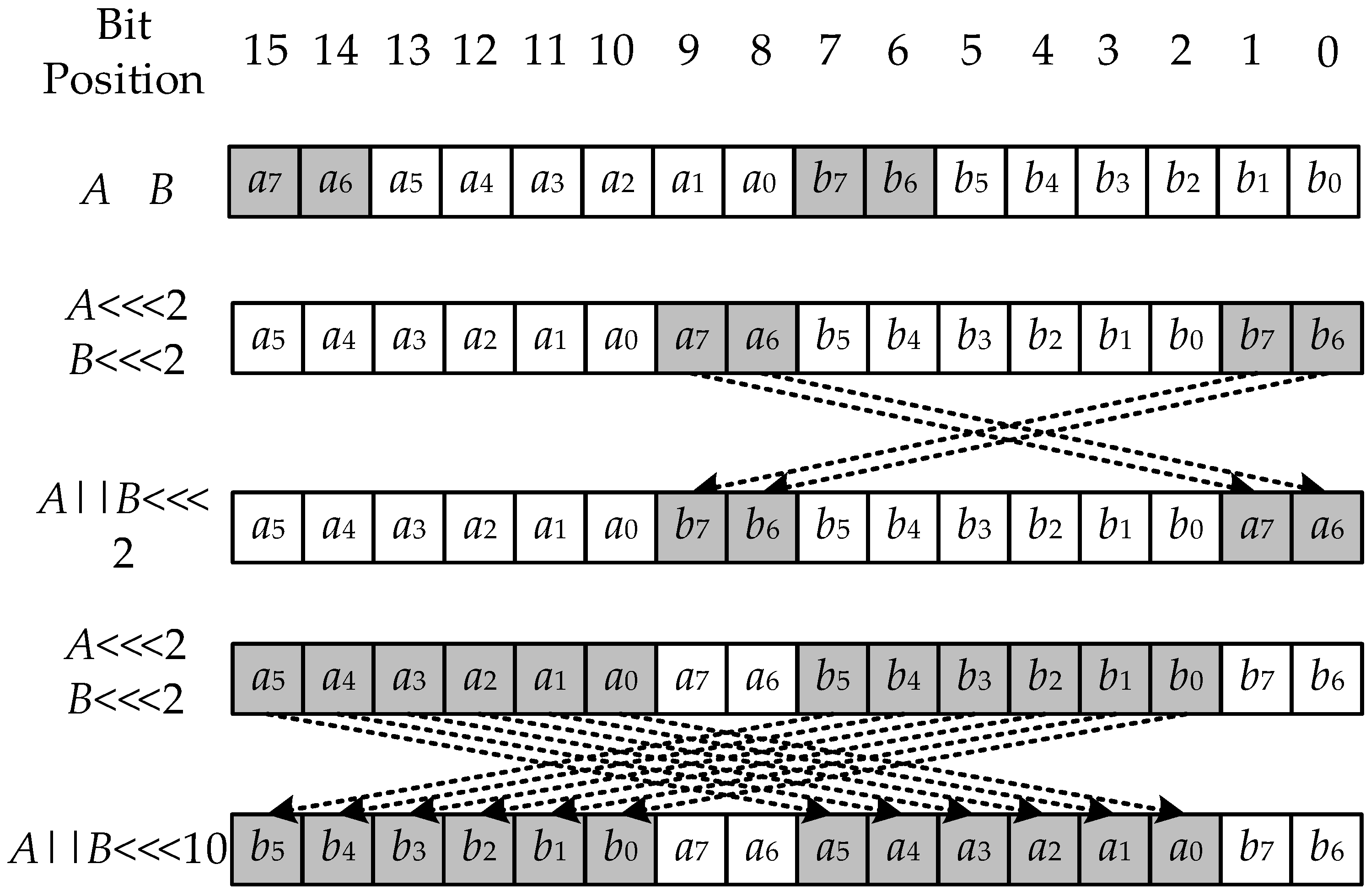
2. Mathematical Analysis of Shift Transformation

2.1. Background for Shift Transformation in Cryptography

The shift is a special bit-level transformation divided into different types. This section introduces some commonly used shift transformations in cryptography. Suppose A is N-bit vector on a linear space F2N, represented as A = {aN−1, aN−2, …, a0}. Let A <<< k and A >>> k denote the left-rotation and right-rotation transformations of A with the k-bits, respectively (0 < k < N). In the left/right-rotation transformation, the bits shifted out from the high/low position are filled into the vacant of the low/high position. Then, the result of the left and right rotation transformation can be expressed by Equations (1) and (2).
A <<< k = {aN−1-k … a0||aN−1aN–k},
A >>> k = {ak−1 … a0||aN−1ak}.
The logical shift transformation omits the data filling, compared with rotation, and directly fills 0. The left and right logical shifts are also the bit-level transformations on the F2N, denoted as A << k and A >> k. Additionally, the result of the logical left and right shift transformation can be expressed by Equations (3) and (4).
A < < k = { a N 1 k     a 0 | | 0 0 × k } ,
A   > >   k = { 0 0 × k | | a N 1     a k } .
In cryptography, a linear transformation, constructed based on rotation and xor operations, is frequently used to achieve effective diffusion in many cryptographic algorithms, such as block cipher algorithms SMS4 [20], HIGHT [21], hash function SHA−2, and so on. Given L is the linear transformation of A on the linear space F2N, L is only composed of rotation and xor operation. L can be generated by Equation (5), where ri is the bit-width of the rotation operation for A, and x is the number of branches of the linear transformation.
L ( A ) = i = 1 x ( A < < < r i ) , 0 r 1 < r 2   < r x N 1 , x N .
Rotation, logical shift, and linear transformation are the three most common shift operations in cryptographic algorithms. Reconstructing them in the same arithmetic logic unit can improve the algorithm implementation efficiency of CGRCA. In addition, some mathematical properties between these operations are analyzed in Section 2.2, which can guide the circuit structure design in Section 3.

2.2. Mathematical Properties of Shift Transformations

Theorem 1.
On the F2N, any k bits right-rotation transformation is equivalent to (N−k) bits left-rotation. The mathematical representation is as follows: A >>> k = A <<< (N−k).
Proof of Theorem 1.
According to Equation (2), vector A1 is the transformation result of the N-bit data A executing a k-bit right rotation transformation. Then, A1 = {ak−1 … a0||aN−1ak}. Based on Equation 1, vector A2 is the transformation result of the N-bit data A executing an (N−k)-bit left rotation. Then, A2 = {aN−1-(N-k) … a0||aN−1aN-(N–k)} = {ak−1 ... a0||aN−1ak}. So, A1 = A2, and A >>> k = A <<< (N−k).
Theorem 2. 
A and B are the vectors on the linear space F2N. On the F22N, the k or (N + k) bit left rotation transformation of vector A||B is Equivalent to the two steps below. First, executing k-bit left rotation transformations for A and B, the results are denoted as A3 and B3. Second, interchanging the lower k-bit of A3 with the lower k-bit of B3 getting A4 and B4 and combining A4 and B4 (denoted as operation RLk); or interchanging the upper (N−k)-bit of A3 with the upper (N−k)-bit of B3 getting A5 and B5, and combining A5 and B5 (denoted as operation RHN-k). The mathematical representations are described as Equations (6) and (7).
R L k ( A < < < k , B < < < k ) = ( A | | B ) < < < k
R H N k ( A < < < k , B < < < k ) = ( A | | B ) < < < ( N + k )
Proof of Theorem 2.
After the first step, the left-rotation results of A and B are defined as A3 = {aN−1-k … a0||aN−1aN-k} and B3 = {bN−1-k … b0||bN−1bN-k}. The interchanging operation RLk exchanges the lower k-bit of A3 with the lower k-bit of B3. So, RLk(A3, B3) = {aN−1-ka0||bN−1bN-k|| bN−1-kb0||aN−1aN-k} = {aN−1-ka0||bN−1b0||aN−1aN-k}. Additionally, (A||B) <<< k = {aN−1-ka0 || bN−1b0 || aN−1aN-k}. It can be concluded that RLk(A <<< k, B <<< k) = (A||B) <<< k. Similarly, RHN-k(A3, B3) = {bN−1-kb0||aN−1aN-k|| aN−1-ka0||bN−1bN-k} = {bN−1-kb0||aN−1a0||bN−1bN-k}, and (A||B) <<< (N + k) = (B||A) <<< k = {bN−1-kb0||aN−1a0||bN−1bN-k}. So, RHN-k(A <<< k, B <<< k) = (A||B) <<< (N + k).□
Figure 1 illustrates Theorem 2. The bit-width of data A and B in Figure 1 are both 8-bit. After 2-bit left-rotation, replace the lower 2-bit of rotation results (a7, a6, and b7, b6), and the result is the same as the value of (A||B) <<< 2. If the replaced data is the upper 6-bit of the rotation result, the interchanging result is consistent with the value of (A||B) <<< 10.
Inference 1.
It can be deduced from Theorems 1 and 2 that any left or right rotation transformation of the vector A||B on F22N is equivalent to the left rotation, regarding the vectors A and B, on the F2N, and an interchanging operation of the two rotation results.
Proof of Inference 1.
on F22N, the shift bit-width of any left rotation, regarding vector A||B, is the form of k or (N + k), 0 ≤ k < N. According to Theorem 2, the k/(N + k)-bit left rotation of vector A||B is equivalent to the left rotation for A and B, and an interchanging operation of the two rotation results. Referencing Theorem 1, there must be a left rotation transformation that can replace the right rotation transformation of A||B on F22N. Therefore, Inference 1 is correct. □
Theorem 3.
On the linear space F2N, any k-bit logical left/right shift transformation can be implemented by a left/right rotation transformation and upper/lower k-bit “and 0” operation. The mathematical expression is as in Equation 8, and the proof is omitted.
{ A < < k = ( A < < < k ) &   1 1 N k   b i t   0 0 k   b i t A > > k = ( A > > > k ) &   0 0 k   b i t   1 1 N k   b i t

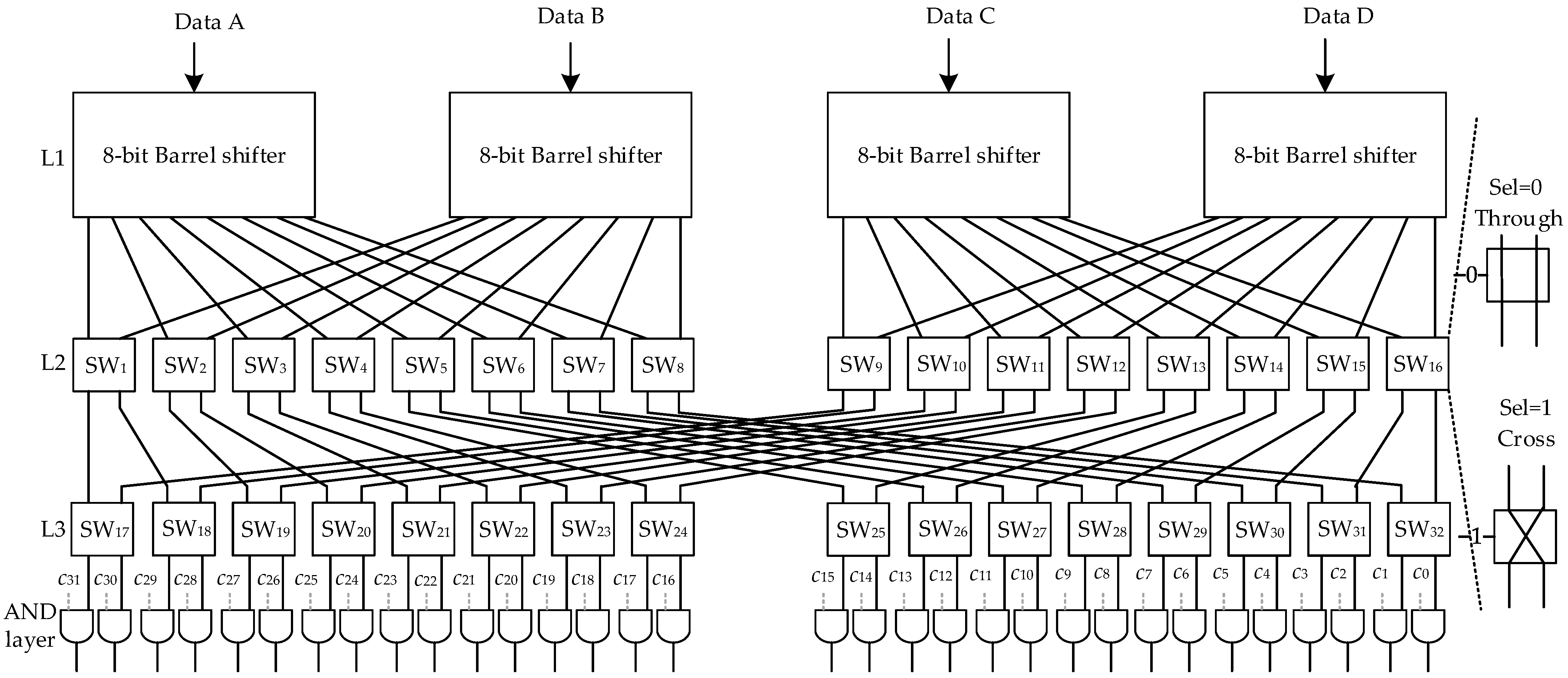
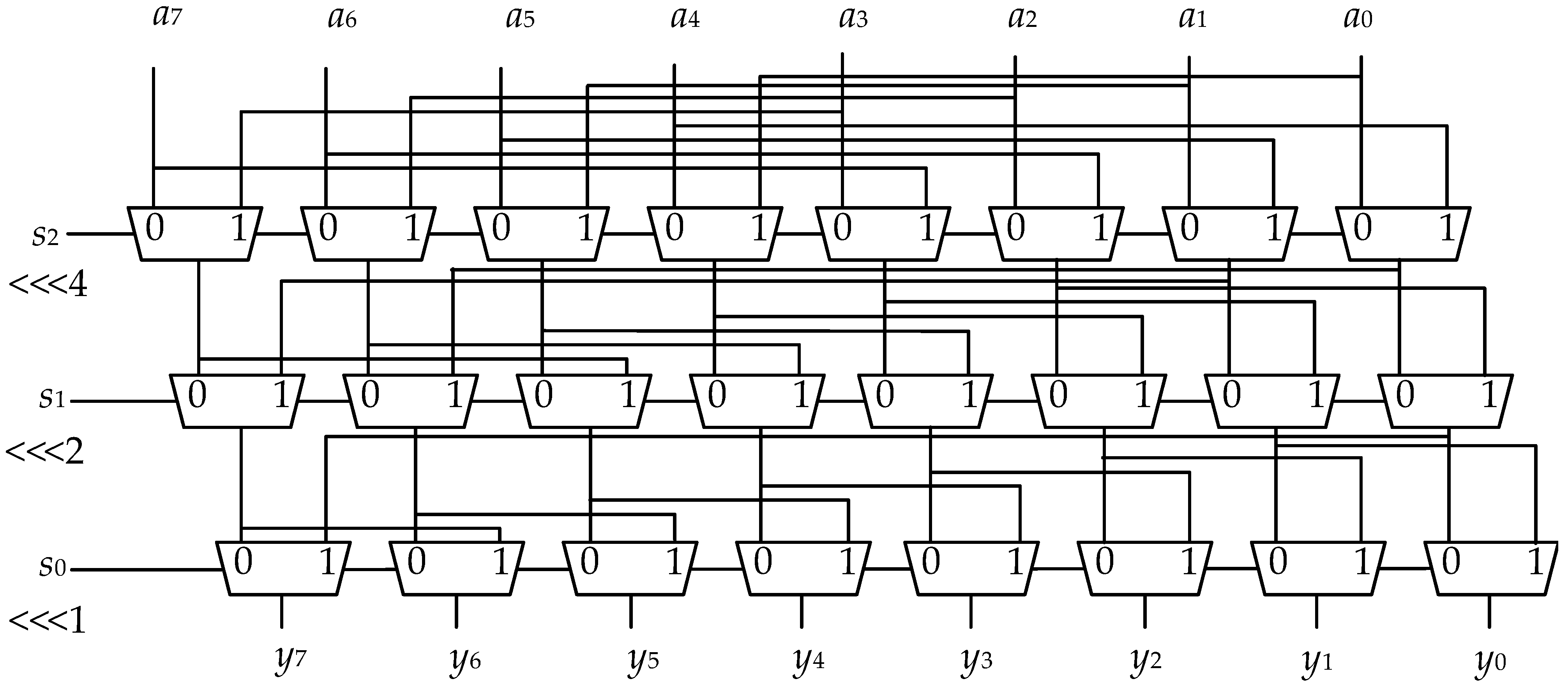
3. Reconfigurable Shift Transformation Unit Design and Data Path Analysis

In this paper, a new type of reconfigurable shift unit (RSTU) is designed based on the above mathematical theorems and inference, including the reconfigurable control bits generation module (CIGM) and reconfigurable data path (RDP). Figure 2 describes the RDP structure of a 32-bit width RSTU, including four 8-bit barrel shifters (BS), several switches (SW), logic gates, and data selectors. Figure 3 illustrates the circuit structure of an 8-bit barrel shifter. The n-bit data input corresponds to the log2n-level selectors, each level has n 2-to-1 data selectors, and the data can be shifted, according to the power of 2, or kept unchanged at each level. One-stage selectors require 1-bit control information, and the n-bit barrel shifter involves log2n-bits control information. In RSTU, the barrel shifters connect to the two-level transmission networks L2, and L3 composed of 16 SW. The circuit function of the SW is equal to two 2-to-1 data selectors with mutually exclusive selection signals. As shown in Figure 2, each SW has two connection states: cross and through. After the data passes through the two-level SW, it enters into the AND layer for logical shift transformation. Changing the control information of this layer can transform any bit of the intermediate value to 0 by the and gates. Next, we introduce how RSTU implements different shift functions by changing the control information.
The following example illustrates the working principle of RDP. When all the four data A, B, C, and D in Figure 2 perform 1-bit left rotation, the control information of each BS is 001, all SW are in the state of through, and all the control information of the AND layer is 1. When A, B and C, D combine into 16-bit data, respectively, to perform a 1-bit left rotation, according to Theorem 2, SW8 and SW16 in L2 should be in the cross-state, which represents that the lower 1-bit of the shift result is exchanged. On this basis, if SW32 or SW17−31 in L3 are in the cross-state, RDP realizes the 1-bit or 17-bit left rotation for 32-bit data A||B||C||D. To sum up, by changing the control information of each SW, RDP can realize shift operation in the form of 4- of 8-bit data in parallel, 2- of 16-bit data in parallel, or 32-bit data. When it is necessary to perform logical shift transformation, based on the above circuit state, setting c0 or c16-c0 to 0 can realize the 1-bit or 17-bit logical left shift for A||B||C||D.
Figure 4 is the linear transformation (LT) computing module that performs linear transformation in RDP, which includes the xor gates, 2-to-1 data selector, and SW. In Figure 4, A–H represents unprocessed data with the same length, A′–H′ is the data via the shift transformation by RDP, A″–H″ is the final output of the LT module, and d0-d14 is the control information. The circuit function performed by the LT module changes when control information is different. For example, when SW33 and SW34 are in the “through” state and the control information d0 and d4 are 1, the output of the LT module is A″=A^A′^B′. If A = B, the RSTU implements the linear transformation (three branches) on data A. When d0 = 0 and d4 = 1, d5 = 1, output B″ = B^A′^B′^C′^D′; when A = B = C = D, RSTU completes a linear transformation on the data B (five branches). If SW33 and SW34 are in the state “cross”, when d0 = d1 = 1 and d7d8 = d9d10 = 01, the outputs of the gates X1, X2, X3, and X4 are combined and sent to X7. As shown by the dotted line in Figure 4, the xor gate X7 outputs through the two ports C″ and D″. At this time, C″||D″ = (A||B)^(A′||B′)^(C′||D′)^(E′||F′)^(G′||H’). When A||B = C||D = E||F = G||H, RSTU implements a linear transformation (five branches) on the merged data A||B. In summary, by changing the control information, RDP can support a linear transformation with a maximum number of branches of five at different granularity.
In addition to RDP, the generation of control information is another focus of the RSTU design. The control information generation of the traditional barrel shifter is simple, which translates the shift bit-width into binary codes. However, the generation is complex and time-consuming for other shifters that support more functions, such as the shifter based on the dynamic multi-stage network [17,18,19]. These shifters support bi-directional rotation and can implement other types of bit-level transformation, such as logical shift, bit extraction, and bit insertion, since the control information corresponding to each function is different, which also increases the complexity of circuit design. For these shifters, the circuit overhead of the control information generation is almost the same as that of the shifter itself. In the next chapter, we will introduce CIGM, in combination with the circuit function and routing algorithms for generating control information. In addition, to adapt the RSTU to the CGRCA architecture, this paper also designs the dedicated configuration word to indicate the RSTU shift function. The configuration word is converted into the control information of RSTU by CIGM.

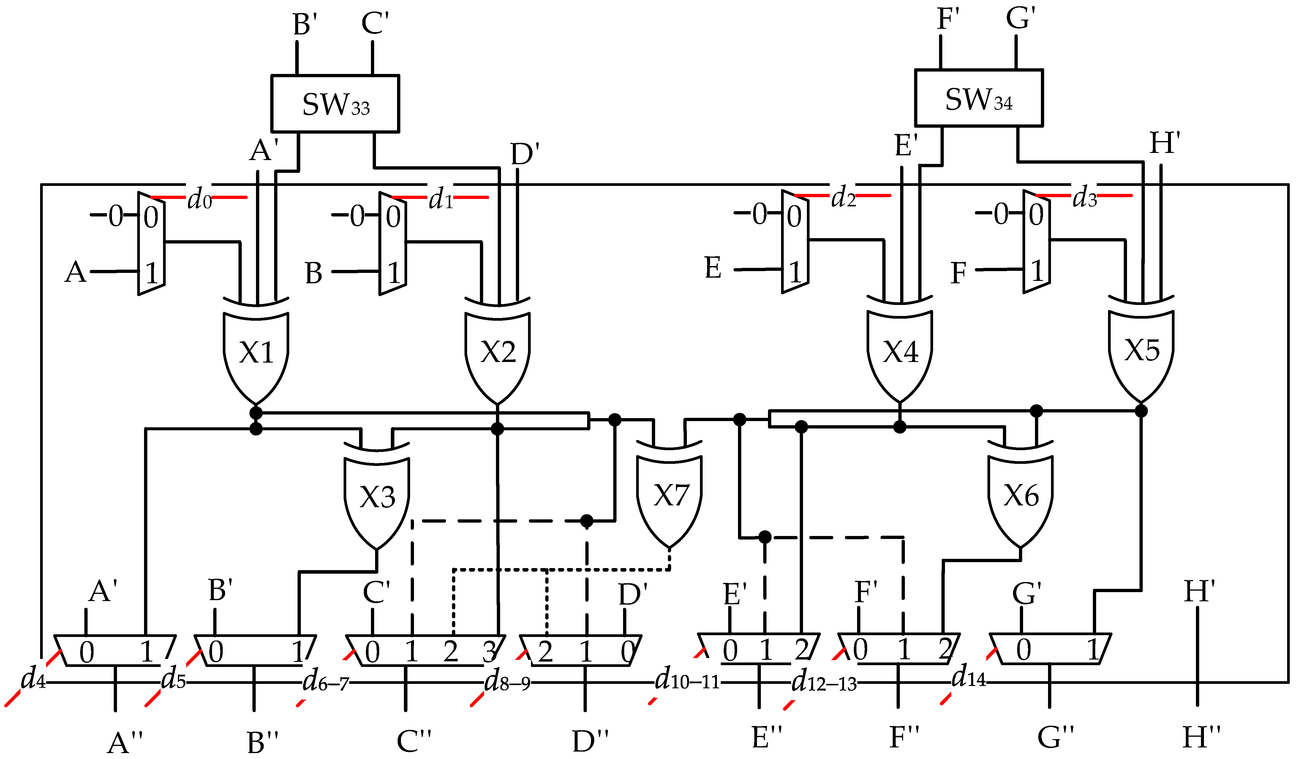
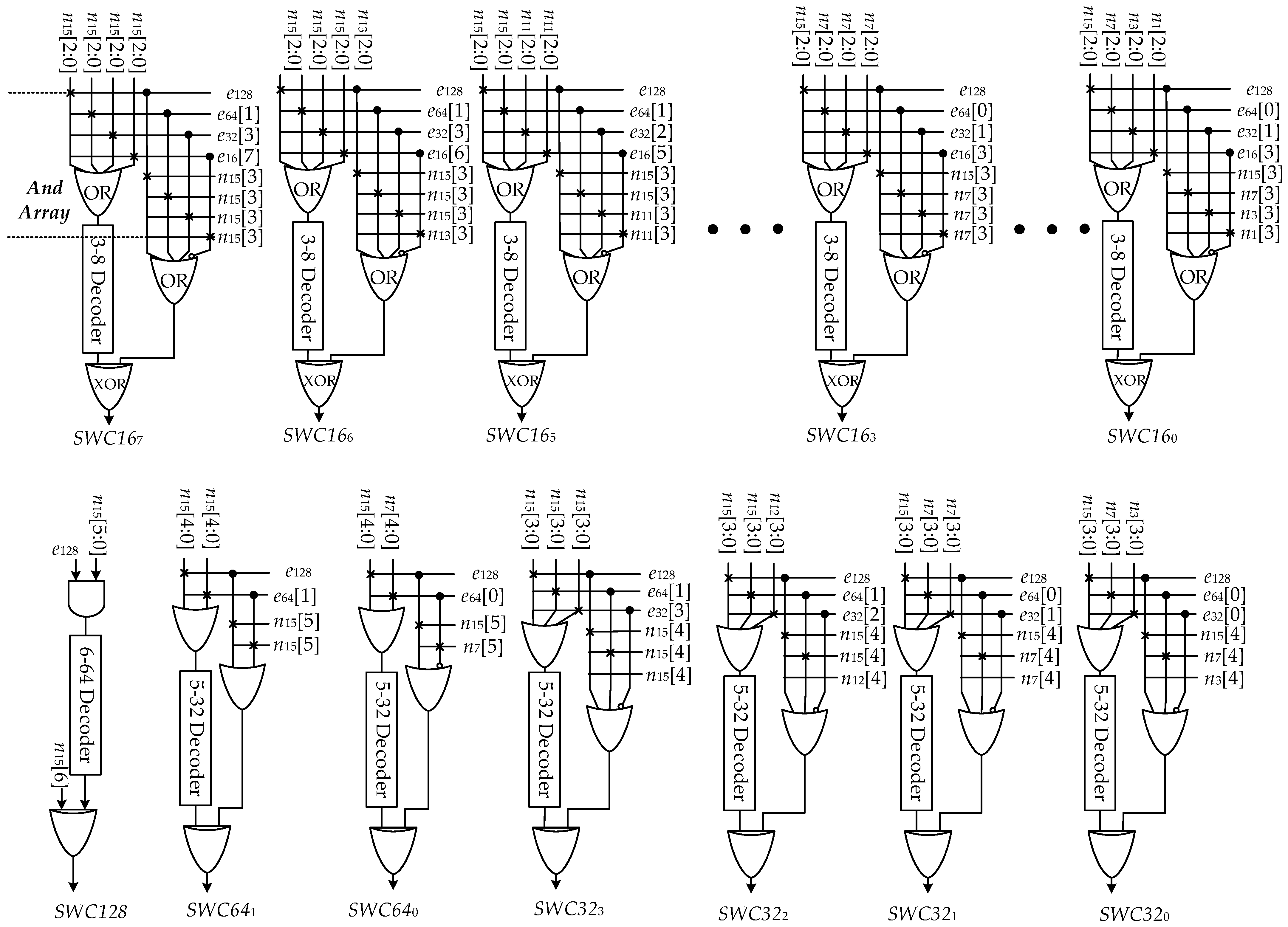
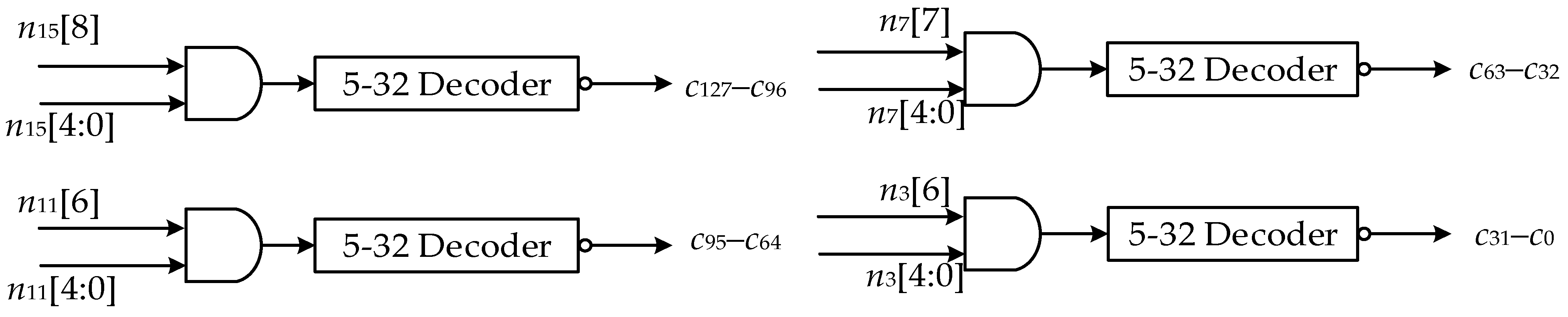
4. Control Information Generating Module Design

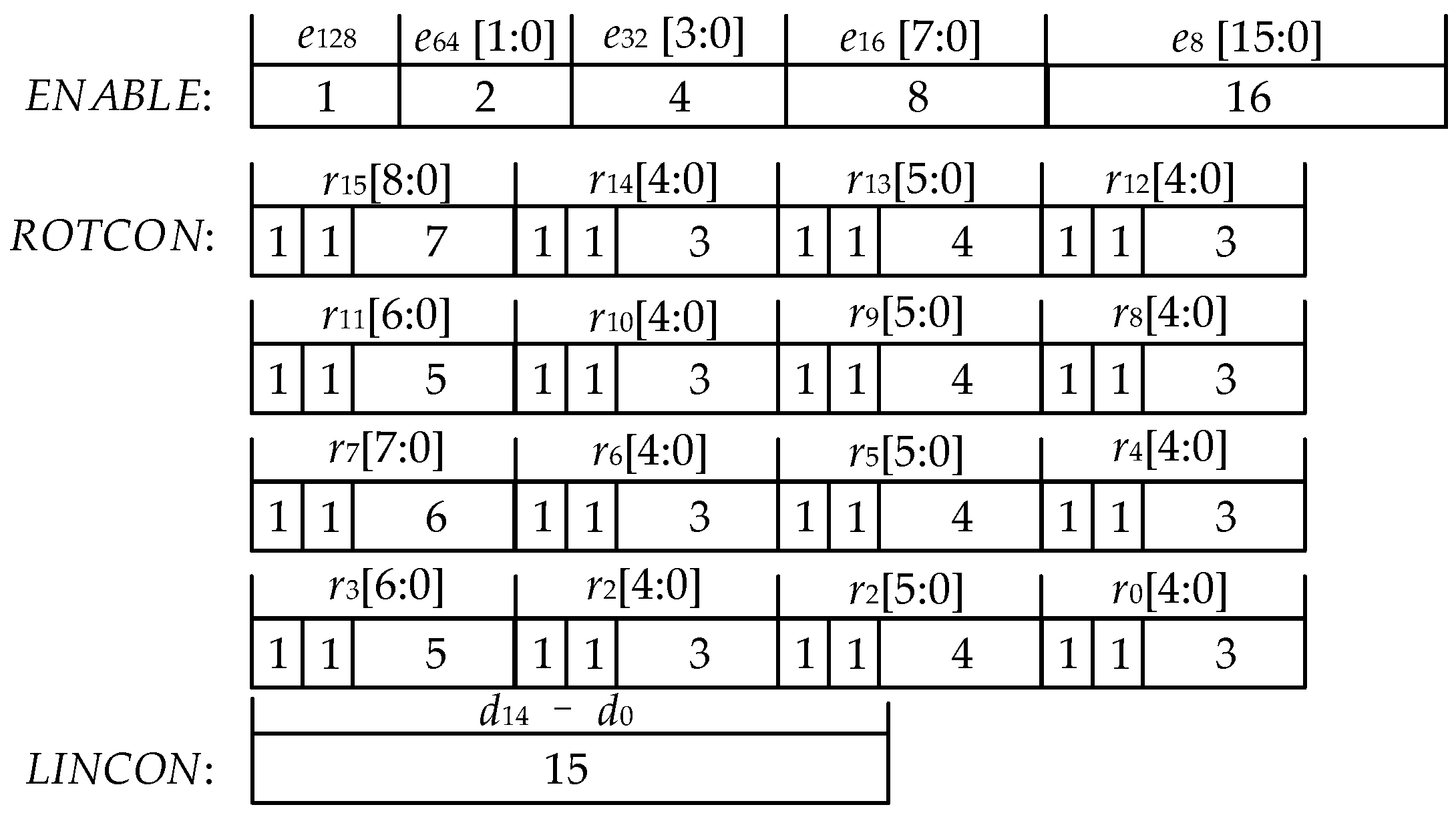
4.1. The Configuration Word Format of RSTU

The RSTU executes different shift functions through switching control information. In most CGRCA, the bit width of a shifter is 128-bit and control information reaches 447 bits, for a 128-bit RSTU. Reconstruction by directly modifying the control information may be hard and requires understanding the circuit structure. Therefore, this paper designs a simplified configuration word and decoding logic (CIGM) to generate control information. Figure 5 shows the format of the configuration word, which involves three fields. The ENABLE field is used to declare the shift granularity of RSTU and contains 31 configuration bits in total. The highest configuration bit is e128. When e128 = 1, the RSTU performs shift operation in the 128-bit granularity. If e128 = 0, continue to check the next two configuration bits: e64 (1:0). The four cases corresponding to different values of e64 (1:0) are listed as follows: 11, RSTU performs two 64-bit shift operations; 10, high 64-bit input performs 64-bit shift operation, and the lower 64-bit input checks the next configuration bits; 01, the lower 64-bit input executes 64-bit shift operation, and the upper 64-bit input checks the subsequent configuration bits; 00, continue to check the next lower four bits: e32 (3:0). By analogy, the ENABLE field instructs the RDP to execute shift operations in different granularities.
The ROTCON field illustrates the specific function of each independent shift operation, including 16 sub-fields r15r0, corresponding to 16-barrel shifters. As the processing granularity of RSTU changes, the valid sub-fields also change. Taking r15 as an example, the highest bit r15 [8] indicates the function of rotation or logical shift, the second highest bit r15 [7] declares a left or right shift, and the remaining 7-bit indicates the bits number of shift operation. When performing a 128-bit shift operation, the seven bits are valid configuration bits, and the rest of the ROTCON sub-fields are invalid. If RSTU performs two 64-bit shift operations, the lower 6-bit of the sub-fields, r15 and r7, are valid, while r14r8 and r6r0 are invalid. When performing 16 8-bit shift operations, the lower three bits of sub-fields r15r0 are the bit-width of 16 shift operations. The LINCON field configures the control information of the LT module, corresponding to d14d0 in Figure 4.

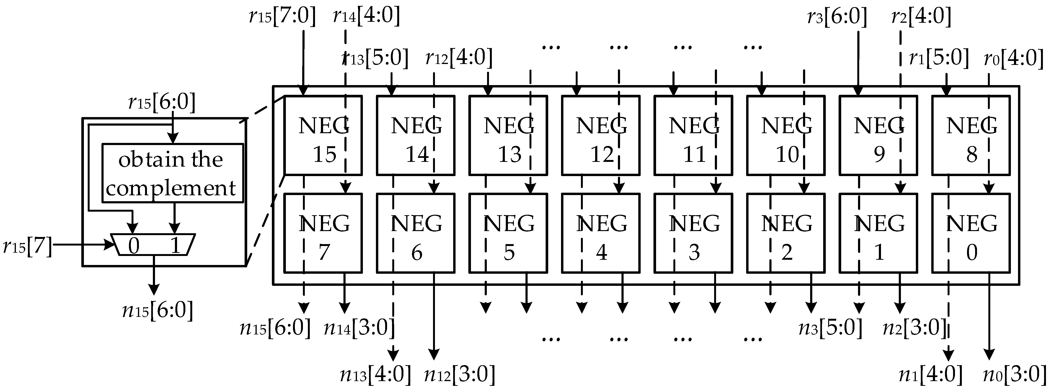
4.2. The Routing Algorithms for Generating Control Information and CIGM Architecture

CIGM consists of four sub-modules, obtaining the complement code module NEG, barrel shifters’ control information (BSC) generation module, SW’ control information (SWC) generation module, and AND layer’s control information (c127c0) generation module. The working principle of each module is as follows. Figure 6 shows the circuit structure of the NEG module, which function is to convert the bit-width of a right rotation in the ROTCON field into the bit-width of the left rotation that produces the same result. Taking r15 as an example, when performing a right-rotation operation, r15[7] = 0, and r15 (7:0) is negative. In contrast, r15 (7:0) is positive if the rotation direction is left (r15[7] = 1). According to Theorem 1, an (Nk)-bit right rotation is equivalent to a k-bit left rotation. When log2N is an integer, the complement of −(N−k) is −k. Therefore, the shift bit-width, represented in the form of left rotation, is the value of removing the highest bit of the complement of r15 (7:0). Record the output of the NEG module as n15n0. Based on the NEG module, this paper proposes routing Algorithm 1 for generating BSC and routing Algorithm 2 for generating SWC. Among them, Algorithm 1 is as follows.
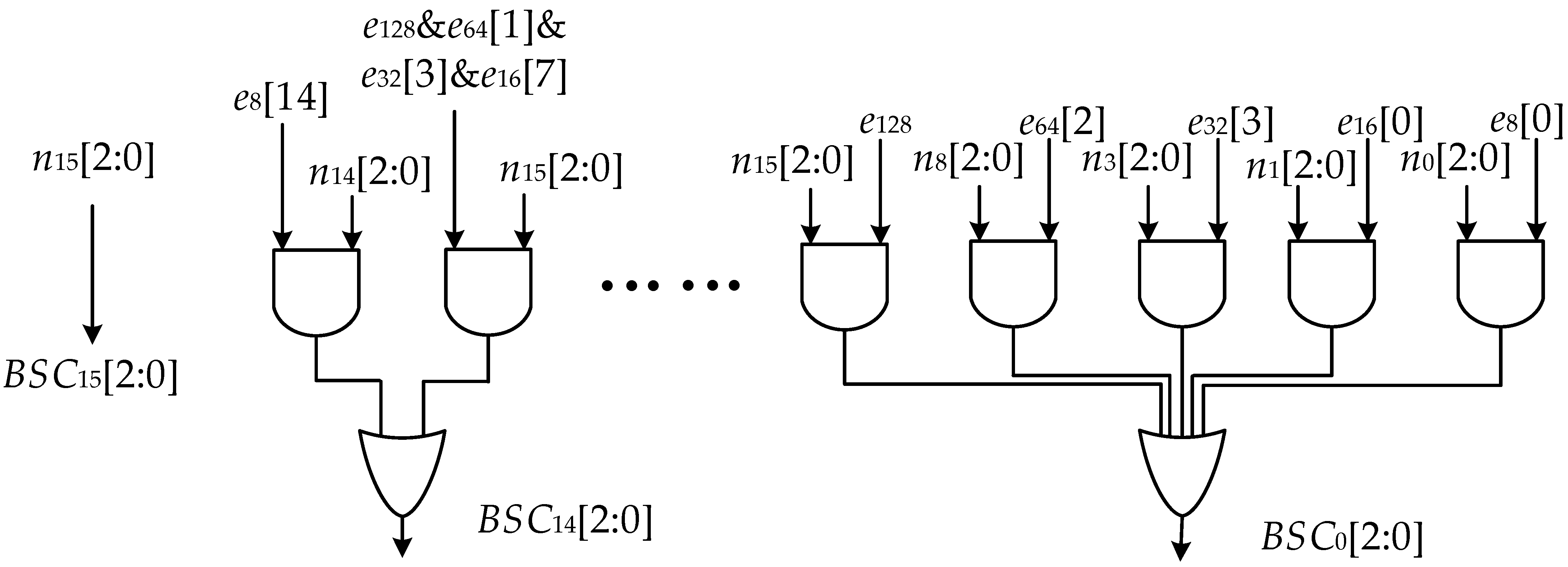
Algorithm 1: The algorithm for generating BSC.
Input: ENABLE, ROTCON, n15n0; Output: BSC15BSC0 (48 bit);
Begin
  • if e128 = 1, BSC15BSC0 = n15[2:0];
  • else if e64[1] = 1, BSC15BSC8 = n15[2:0], if e64[0] = 0, BSC7BSC0 = n7[2:0];
  • else if e32[3] = 1, BSC15BSC12 = n15[2:0], if e32[2] = 1, BSC11BSC8 = n11[2:0], if e32[1] = 1, BSC7BSC4 = n7[2:0], if e32[0] = 1, BSC3BSC0 = n0[2:0];
  • else if e16[7] = 1, BSC15BSC14 = n15[2:0], if e16[6] = 1, BSC13BSC12 = n13[2:0], if e16[5] = 1, BSC11BSC10 = n10[2:0], if e16[4] = 1, BSC9BSC8 = n9[2:0], if e16[3] = 1, BSC7BSC6 = n7[2:0], if e16[2] = 1, BSC5BSC4 = n5[2:0], if e16[1] = 1, BSC3BSC2 = n3[2:0], if e16[0] = 1, BSC1BSC0 = n15[2:0];
  • else if e16[7] = 1, BSC15BSC14 = n15[2:0], if e16[6] = 1, BSC13BSC12 = n13[2:0], if e16[5] = 1, BSC11BSC10 = n10[2:0], if e16[4] = 1, BSC9BSC8 = n9[2:0], if e16[3] = 1, BSC7BSC6 = n7[2:0], if e16[2] = 1, BSC5BSC4 = n5[2:0], if e16[1] = 1, BSC3BSC2 = n3[2:0], if e16[0] = 1, BSC1BSC0 = n15[2:0];
  • else BSCi = ni [2:0];
  • end if.
END
The input of Algorithm 1 includes the configuration word (ENABLE and ROTCON) and output of NEG (n15n0). The 16 barrel shifters (BS15−BS0) control information in the 128-bit RSTU BSC15BSC0 from high bit position to low. According to Inference 1, supposing the rotation bit-width is more than eight bits, RSTU implements the long bit-width shift via changing the state of switches, so that BSC is unchangeable. So, BSC can directly take the last three bits of the complement generated by NEG. For step 1 of Algorithm 1, when e128 = 1, RSTU works in 128-bit granularity. The control information of BSC is the same, which is the lower three bits of n15. Otherwise, go to step 2. If e64 (1:0) = 11, RSTU executes two 64-bit shift operations. BSC15BSC8 takes the value n15 (2:0), and BSC7BSC0 is equal to n7 (2:0). If any bit of e64 is 0, the algorithm enters step 3 to judge the configuration bits e32 (3:0) and, finally, obtain all BSC. Figure 7 shows part of the structure of the BSC generation circuit. In any shift mode, the value of BSC15 is n15 (2:0). The value of BSC14 may be n15 or n14, which depends on the configuration words. If the input of BS14 shifts in the granularity of 128-, 64-, 32-, or 16-bit, BSC14 = n15, while executing an 8-bit shift operation, BSC14 = n14. More complicated, the value of BSC0 ranges from the five outputs of NEG, and its generation logic requires five and and one or gates.
The 128-bit RSTU contains a four-level SW, denoted as L−128, L−64, L−32, and L−16, and routing algorithms of group 2, below, generate their control information. The input of the SWC generation circuit is similar to BSC, including ENABLE, ROTCON, and n15n0. Figure 8 shows the relationship among the switches, control information, and routing algorithms. In Figure 8, each level of SW requires 64-bit control information, named 64-bit SWC128, 32-bit SWC641SWC640, 16-bit SWC323−SWC320, and 8-bit SWC167SWC160, according to the location of switches, which are generated by different routing sub-algorithms 2.1, 2.21−2.22, 2.31−2.34, and 2.41–2.48. Next, take Sub-Algorithm 2.1 as an example to introduce how Algorithm 2 generates SWC.
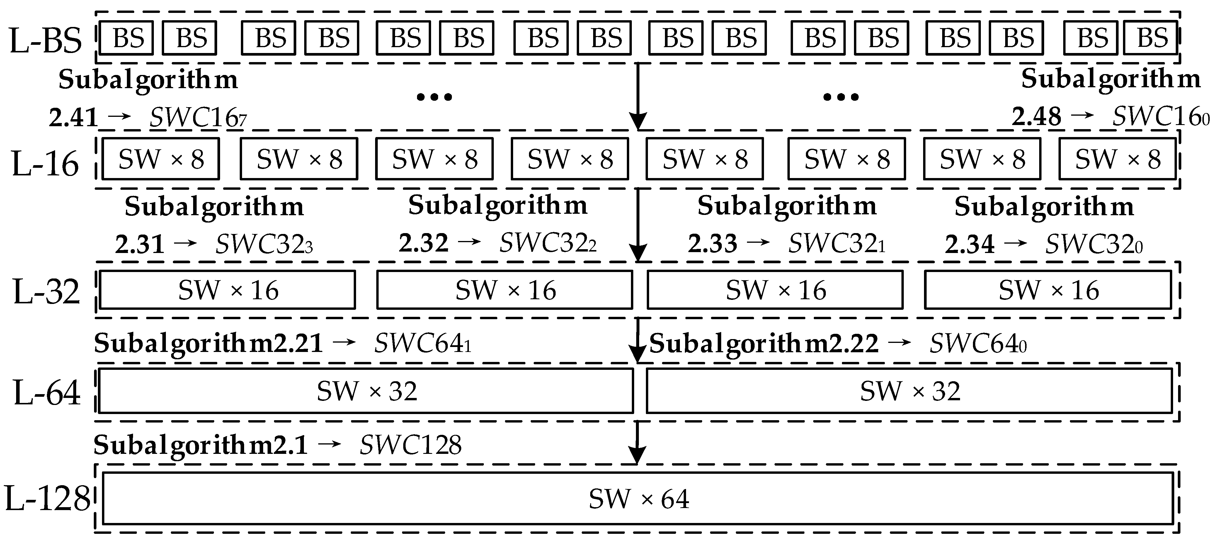
Algorithm 2: The algorithms for generating SWC
Input: ENABLE, ROTCON, n15−n0; Output: SWC128, SWC64, SWC32, SWC16 (256 bit);
Sub-Algorithm 2.1. Begin:
  • if e128 = 1;
  • if n15[7:6] = 01 or 10, SWC128 = DEC(n15[5:0]);
  • else SWC128 = INV(DEC(n15[5:0]));
  • end if;
  • else SWC128 = 0;
  • end if.
End
Sub-Algorithm 2.21; Sub-Algorithm 2.22;
……
Sub-Algorithm 2.48. Begin:
  • if e128 = 0;
  • if n15[3] = 0, SWC160 = DEC(n15[2:0]);
  • else SWC160 = INV(DEC(n15[2:0]));
  • end if;
  • else if e64[0] = 1;
  • if n7[3] = 0, SWC160 = DEC(n7[2:0]);
  • else SWC160 = INV(DEC(n7[2:0]));
  • end if;
  • else if e32[0] = 1;
  • if n3[3] = 0, SWC160 = DEC(n3[2:0]);
  • else SWC160 = INV(DEC(n3[2:0]));
  • end if;
  • else if e16[0] = 1;
  • if n1[3] = 1, SWC160 = DEC(n1[2:0]);
  • else SWC160 = INV(DEC(n1[2:0]));
  • end if;
  • else SWC160 = 0;
  • end if;
End
Firstly, step 1 checks whether the RSTU works in 128-bit shift mode. If yes, go to step 2. Secondly, steps 2 and 3 use the decoding function DEV and the inverse function INV to obtain SWC128, according to the value of n15. DEV function translates the n-bit binary number d into 2n-bit data D. D consists of (2n−d)-bit 0 and d-bit 1 from the highest bit position to the lowest. Taking the 3-bit left rotation in the 128-bit granularity as an example, in this case, n15 [6] = 0 and n15 (5:0) = 000011. Next, execute step 2; the output of the DEV function is 64-bit SWC128: 0...0111, which means the lower three switches are in the cross-state. According to Theorem 2, the circuit realizes a 3-bit left rotation; if n15[6] = 1, execute step 3. The INV function will invert all input bits, and the output result is 64-bit SWC128: 1...1000. The upper 61 switches of L−128 are in the cross-state, realizing a 67-bit left rotation. Finally, if e128 = 0, which means that the RSTU is working in other shift modes, all SW of L-128 are in the through state and SWC128 = 0. By analogy, we can conclude the routing algorithms of other SWC, except for Sub-Algorithm 2.1. This paper provides Sub-Algorithm 4.48, with a more complicated execution process. The execution process can be summarized as two steps.
  • Judge which shift mode the RSTU works in through ENABLE.
  • Leverage the DEV and INV functions to generate the control information SWC160, in combination with the corresponding ROTCON sub-fields.
Figure 9 depicts part of the circuit structure for SWC generation. The SWC128 generation circuit is composed of an and gate, 6-to-64 decoder, and xor gate. The decoder realizes the function of DEC. When RSTU works in 128-bit shift mode, e128 is high level, and the and gate is similar to a direct connection. If n15[6] is low level, it means that the shift bit-width is less than 64, and the xor gate transmits the decoder outputs. When n15[6] is high level, the number of shift bits is greater than 64, and the xor gate inverts the decoder outputs as the control information. If RSTU works in other shift modes, e128 is low level, the and gate outputs 0, and all switches of L−128 remain in the through state. Other SWC generating processes are similar to SWC128, including four steps.
  • Leverage the and gates array and ENABLE configuration bits to set the unused complement to 0;
  • Input all the results of and array through the or gate to obtain the input of the decoder;
  • Decode the complement to get SWC.
  • Adjust the difference caused by the shift bit-width through the xor gate.
Figure 10 shows the control information generation module of the and layer. RSTU supports the logical shift in 32-bit granularity. The control information of every 32 and gate is composed of one and gate and 5–32 decoders, similar to the SWC. Different from the generation module, the function of the decoder is to translate the 5-bit binary input into 32-bit decimal output, according to the principle of filling “0” from the lowest position.

5. Functional and Performance Analysis

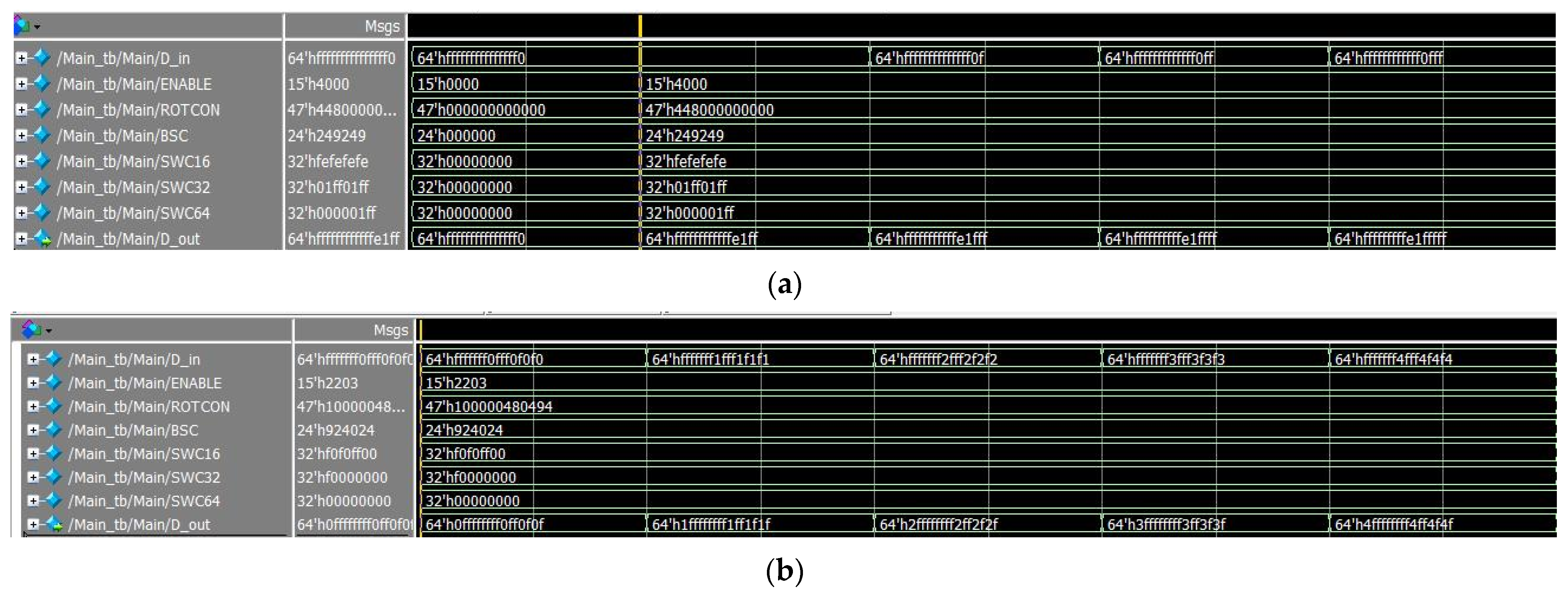
5.1. Functional Test and Comparison

To easily compare with the reconfigurable shifters in the other literature, this paper sets the bit-width of RSTU to 64 bits. A 64-bit RSTU is implemented in Xilinx’s FPGA, leveraging ISE Design Suite 14.7 (Xilinx, San Jose, CA, USA) and Modelsim 10.4 (Mentor Graphics, Wilsonville, OR, USA) to test the function coverage. Figure 11 gives the signal flow of some of the simulation results, where D_in is 64-bit input, D_out is the transformation result, and the other signals are configuration words and control information related to execution. For the first group excitation vectors, the configuration words ENABLE and ROTCON instruct RSTU to execute a 9-bit left rotation for D_in. At this point, each barrel shifter shifts 1-bit to the left. Four SW16 realize the interchanging of the upper seven bits of two 8-bit intermediate values. Two SW32 implement the interchanging of the lower nine bits of two 16-bit intermediate values. SW64 interchanges the lower 9-bit of two 32-bit intermediate values (BSC and SWC expressed in hexadecimal format). The final result shows that the D_out = D_in <<< 9 function execution is correct.
For the second group excitation vectors, ENABLE and ROTCON have stated that RSTU implements a 4-bit right rotation for the upper 32-bit of D_in, an 8-bit left rotation of D_in [31:16], and two 4-bit left rotation of the lower octet and next lower octet of D_in. The generated BSC and SWC are shown in Figure 11b. The eight-barrel shifters shift to the left by four, four, four, four, zero, zero, four, and four bits, respectively. Four SW16 respectively execute the functions of upper 4-bit interchanging, upper 4-bit interchanging, 8-bit interchanging, and pass-through. One SW32 interchanges the upper 4-bit of the 16-bit intermediate results. The other SW32 and SW64 gets past the input. The final result shows that the D_out = {D_in [63:32] <<< 4||D_in [31:16] <<< 8||D_in [15:8] <<< 4||D_in [7:0] <<< 4} function execution is correct.
This paper compares the shift operations supported by RSTU with the typical reconfigurable shifters [17,18,19]. Table 1 shows the experimental results. The first column in Table 1 lists various shift operations, and the first row shows the compared shifters, including the classic barrel, Chang’s (2013), Hilewitz’s (2009), and Ma’s (2018) shifters, designed based on the inverse butterfly network and RSTU proposed in this paper. Hilewitz’s shifter (2009) unifies the traditional shift operations and complex bit-level operations (bit extraction, bit insertion, and bit classification) under one architecture. However, the algorithm for generating control information is recursive, and the control information generates serially, which is time-consuming to execute. Additionally, when the levels of the network increase, the algorithm complexity will increase sharply. Chang et al. (2013) propose a control information generation algorithm executed in parallel, improving the shifter performance. Ma’s shifter (2018) is based on the parallelized control information generation algorithm, too. Moreover, the shifter supports bidirectional rotation and multiple parallel short-word shift operations with a bit-width of 2i (i = 1, 2, …, log2(n)). Their control information is generated by a normalized algorithm, which further reduces the circuit area.
We realize two types of RSTU listed in the last two columns, based on whether integrate the LT module or not. The results show that all shifters support 64-bit bidirectional rotation. However, barrel shifters can only implement a logical shift in a single direction. Chang’s (2013) and Hilewitz’s (2009) shifters support bidirectional 64-bit rotation. Ma’s shifter (2018) is more flexible and supports more shift operations in different granularity. However, except for the RSTU with the LT module, the other shifters do not support linear transformation. Although the linear transformation is not essential for their application, it becomes an advantage of RSTU when applied to reconfigurable cryptographic processors, which means RSTU supports some extended shift-type operations. So, from the point of shift function, the RSTU is more powerful.

5.2. Performance Comparisons and Analysis

Furthermore, we synthesize RSTU to the gate level by using the EDA software mapping to the 65-nm standard cell library, optimizing for the shortest latency and minimum area. From the literature [18,19], the Chang’s (2013) and Ma’s (2018) shifters are synthesized in the same implementation environment (process 1.0, temperature −40 °C, voltage 1.08 V, and CMOS 65 nm) with RSTU. However, the technology used in Hilewitz’s shifter (2009) is different from other shifters, thus leading the comparison of the absolute area and delay to be meaningless. So, we take the barrel shifter in the same implementation environment as a benchmark, and the area (relative area) and delay (relative delay) ratios between the compared shifter and barrel shifter is the reference data shown in columns 4 and 6 of Table 2.
The barrel shifter used for comparing with RSTU, Chang’s shifter (2013), and Ma’s shifter (2018) is coded together with RSTU in the same environment. Additionally, the parameters of the barrel shifter, as a benchmark for Hilewitz’s shifter (2009), are obtained from the literature [17]. In addition to the relative delay and area, we also put the product of the two into the experimental comparison and list them in the last column of Table 2, named the area-delay product (ADP). The smaller the ADP, the more objectively it can explain the shifter advantages on the performance. Table 2 summarizes the experimental results.
The experimental results show that RSTU has advantages in relative delay, compared with other shifters. The reason is that RSTU abandons other bit-level functions (bit extraction, bit classification, etc.), so that the routing algorithms execute fast. On the other hand, the relative area of RSTU is almost the same as Hilewitz’s Shifter (2009) and reduced by 13%, compared to Chang’s shifter (2013). The reason is that the control information generation circuit of Hilewitz’s Shifter consumes lots of hardware resources, while Chang’s shifter has optimized the circuit overhead by utilizing parallelization. Compared with Ma’s shifter (2018), supporting the same function, RSTU’s relative area and delay reduce by 18.2% and 11.8%. Based on Chang’s shifter, Ma’s shifter unifies the routing algorithms and implements them under the same architecture, which brings improved delay and larger overhead. In addition, Ma et al. also proposed a basic shifter that does not support other shift operations, except for 64-bit granularity. The relative delay and area under this scheme are only 1.08 and 1.04, which illustrates that, to support multi-granularity shift operations, the overhead of the control information generation circuit is significantly more extensive. Finally, the ADP improvement of RSTU is 24.6%, 18.1%, and 1.32%, compared to the other three shifters, which confirms an acceptable circuit cost–performance ratio of RSTU in implementing shift operations.
We have counted the shift operations in the existing cryptographic algorithms. The statistical results of some typical algorithms are shown in Table 3, below. From Table 3, the bit-width of the shift operations in different algorithms is varied. Therefore, RSTU can be widely used in implementing different cryptographic algorithms by reconstructing granularity. Furthermore, with the upgrade of cryptographic algorithms, it is possible to emerge a combination of two 8-bit and one 16-bit shift operations in a 32-bit operator. RSTU can also support this shift operation to match future cryptography requirements. The support for various types of shift operations proves that the flexibility of RSTU can meet different application environments. Moreover, the data path of RSTU is a typical recursive structure. According to the requirements of cryptographic applications, the processing bit-width of RSTU can be easily extended to any 2i bits.
In conclusion, if RSTU is integrated into CGRCA, it has functional and area-efficiency advantages over other shifters. However, when applied to general-purpose processors, RSTU designed for cryptographic computing cannot realize the other bit-level transformation supported by other shifters. So, RSTU is unsuitable for application to general-purpose computing, which is a disadvantage.

6. Conclusions

This paper first analyzes the mathematical properties of shift transformations in cryptography. Based on this, a reconfigurable shift unit RSTU is proposed that supports multiple shift operations in different granularity, based on the barrel shifter and switches. Moreover, we designed the configuration word and routing algorithms to generate control information for RSTU and implement the control information generation module. Compared with other reconfigurable shifters designed for bit-permutation transformation, the proposed shift unit covers more shift-type operations. The experimental results show that, due to the focus on the realization of shift operations in the circuit structure, the processing speed of RSTU is increased by 9.9%~18.2%, compared with other similar shifters, and the relative area is reduced by, at most, 13%. To sum up, RSTU has high functional coverage and good area efficiency. Our shifter realizes the transformation of the reconfigurable shifter from the shift bit-width configurable to the shift granularity configurable.

Author Contributions

Conceptualization, T.Q., Z.D. and Y.L.; methodology, T.Q. and L.C.; formal analysis, T.Q. and L.C.; investigation, Y.L.; resources, Z.D.; writing—original draft preparation, T.Q., Y.L. and L.C.; writing—review and editing, T.Q. and Z.D.; visualization, T.Q. and Z.D.; supervision, Z.D.; project administration, Z.D. and L.C. All authors have read and agreed to the published version of the manuscript.

Funding

This research received no external funding.

Data Availability Statement

All data included in this study are available upon request by contacting qutongzhou@outlook.com.

Conflicts of Interest

The authors declare no conflict of interest.

References

  1. Wijtvliet, M.; Waeijen, L.; Corporaal, H. Coarse Grained Reconfigurable Architectures in The Past 25 Years: Overview and Classification. SAMOS 2017. In Proceedings of the 2017 International Conference on Embedded Computer Systems: Architectures, Modeling and Simulation, Agios Konstantinos, Greece, 17–21 July 2016; pp. 235–244. [Google Scholar] [CrossRef]
  2. Zhu, J.; Wei, S.; Liu, L.; Li, Z. Reconfigurable computing: Toward software defined chips. Sci. Sin. Inf. 2020, 50, 1407–1426. [Google Scholar] [CrossRef]
  3. Bossuet, L.; Grand, M.; Gaspar, L.; Fischer, V.; Gogniat, G. Architectures of Flexible Symmetric Key Crypto Engines--A Survey: From Hardware Coprocessor to Multi-crypto-processor System on Chip. Acm Comput. Surv. 2013, 45, 1–32. [Google Scholar] [CrossRef]
  4. Gokhan, S.; Derek, C. Cryptoraptor: High Throughput Reconfigurable Cryptographic Processor. ICCAD 2014. In Proceedings of the 2014 International Conference on Computer Aided Design, San Jose, CA, USA, 2–6 November 2014; pp. 155–161. [Google Scholar] [CrossRef]
  5. Liu, L.; Wang, B.; Deng, C.; Zhu, M.; Yin, S.; Wei, S. Anole: A Highly Efficient Dynamically Reconfigurable Crypto-Processor for Symmetric-Key Algorithms. IEEE Trans. Comput. Aided Des. Integr. Circuits Syst. 2018, 37, 3081–3094. [Google Scholar] [CrossRef]
  6. Deng, C.; Wang, B.; Liu, L.; Zhu, M.; Wu, Y.; Li, H.; Yin, S.; Wei, S. A 60 Gb/s-Level Coarse-Grained Reconfigurable Cryptographic Processor with Less Than 1W Power. IEEE Trans. Circuits Syst. II Express Briefs 2019, 67, 375–379. [Google Scholar] [CrossRef]
  7. Wang, B.; Liu, L.B. A Flexible and Energy-Efficient Reconfigurable Architecture for Symmetric Cipher Processing. ISCS 2015. In Proceedings of the 2015 IEEE International Symposium on Circuits and Systems, Lisbon, Portugal, 24–27 May 2015; pp. 1182–1185. [Google Scholar] [CrossRef]
  8. Du, Y.; Li, W.; Dai, Z.; Nan, L. PVHArray: An Energy-Efficient Reconfigurable Cryptographic Logic Array with Intelligent Mapping. IEEE Trans. Very Large Scale Integr. Syst. 2020, 28, 1302–1315. [Google Scholar] [CrossRef]
  9. Jinjiang, Y.; Wei, G.; Peng, C.; Jun, Y. An Area-Efficient Design of Reconfigurable S-box for Parallel Implementation of Block Ciphers. IEICE Electron. Express 2016, 13, 20160138. [Google Scholar] [CrossRef]
  10. Nan, L.; Zeng, X.; Wang, Z.; Du, Y.; Li, W. Research of a Reconfigurable Coarse-Grained Cryptographic Processing Unit Based on Different Operation Similar Structure. ASICON 2017. In Proceedings of the 2017 IEEE 12th International Conference on ASIC, Guiyang, China, 25–28 October 2017; pp. 191–194. [Google Scholar] [CrossRef]
  11. Bansod, G.; Raval, N.; Pisharoty, N. Implementation of a New Lightweight Encryption Design for Embedded Security. IEEE Trans. Inf. Secur. 2014, 10, 142–151. [Google Scholar] [CrossRef]
  12. Jolfaei, A.; Wu, X.W.; Muthukkumarasamy, V. On the Security of Permutation-Only Image Encryption Schemes. IEEE Trans. Inf. Secur. 2015, 11, 235–246. [Google Scholar] [CrossRef]
  13. Schwartz, S. Human–Mouse Alignments with BLASTZ. Genome Res. 2003, 13, 103–107. [Google Scholar] [CrossRef] [PubMed]
  14. Sanchez, A.C.; Sanchez, R.R. The Rijndael Block Cipher (AES proposal): A Comparison with DES. Iccst 2001. In Proceedings of the IEEE 35th Annual 2001 International Carnahan Conference on Security Technology, London, UK, 16–19 October 2001; pp. 229–234. [Google Scholar] [CrossRef]
  15. Orhanou, G.; El Hajji, S.; Lakbabi, A.; Bentaleb, Y. Analytical Evaluation of The Stream Cipher ZUC. ICMCS 2012. In Proceedings of the IEEE 12th International Conference on Multimedia Computing & Systems, Tangiers, Morocco, 10–12 May 2012. [Google Scholar] [CrossRef]
  16. Suhaili, S.B.; Watanabe, T. Design of High-Throughput SHA-256 Hash Function Based on FPGA. ICEEI 2017. In Proceedings of the 2017 6th International Conference on Electrical Engineering and Informatics, Langkawi, Malaysia, 25–27 November 2017; pp. 1–6. [Google Scholar] [CrossRef]
  17. Chang, Z.; Dai, Z. Research on Extract-Shift-Reverse Routing Algorithm in Inverse Butterfly Network. CISCE 2017. In Proceedings of the International Conference on Communications, Information System and Computer Engineering, Haikou, China, 5–7 July 2019; pp. 206–209. [Google Scholar] [CrossRef]
  18. Hilewitz, Y.; Lee, R.B. A New Basis for Shifters in General-Purpose Processors for Existing and Advanced Bit Manipulations. IEEE Trans. Comput. 2009, 58, 1035–1048. [Google Scholar] [CrossRef]
  19. Ma, C.; Dai, Z.-B.; Li, W.; Zang, H.-J. A Highly Efficient Reconfigurable Rotation Unit Based on an Inverse Butterfly Network. Front. Inform. Technol. Electron. Eng. 2017, 18, 1784–1794. [Google Scholar] [CrossRef]
  20. Wu, C.; Tang, Y.; Wei, Y. A design of high-Speed SMS4 cipher circuit. AMTEI 2021. In Proceedings of the International Conference on Advanced Manufacturing Technology and Electronic Information, Zhuhai, China, 5 November 2021. [Google Scholar]
  21. Hong, D.; Sung, J.; Hong, S.; Lim, J.; Lee, S.; Koo, B.-S.; Lee, C.; Chang, D.; Lee, J.; Jeong, K.; et al. HIGHT: A New Block Cipher Suitable for Low-Resource Device. CHES 2016. In Proceedings of the International Workshop on Cryptographic Hardware and Embedded Systems, Yokohama, Japan, 10–13 October 2006; pp. 46–59. [Google Scholar] [CrossRef] [Green Version]
Figure 1. Implementation principles of N-bit shift transformation based on N/2-bit rotation and interchanging operations.
Electronics 11 03144 g001
Figure 2. The reconfigurable data path of 32-bit RSTU.
Electronics 11 03144 g002
Figure 3. The circuit structure of the 8-bit barrel shifter.
Electronics 11 03144 g003
Figure 4. The circuit structure of the linear transformation processing module.
Electronics 11 03144 g004
Figure 5. The format of RSTU configuration word.
Electronics 11 03144 g005
Figure 6. The circuit structure of the NEG module.
Electronics 11 03144 g006
Figure 7. Part of the circuit structure for generating BWC.
Electronics 11 03144 g007
Figure 8. The relationships among the switches, control information, and routing algorithms.
Electronics 11 03144 g008
Figure 9. Part of the circuit structure for generating SWC.
Electronics 11 03144 g009
Figure 10. Generating module of the AND layer control information.
Electronics 11 03144 g010
Figure 11. (a) The signal flow of RSTU executing a 9-bit left rotation operation for D_in. (b) The Signal flow of RSTU executing a 4-bit right rotation for the upper 32-bit of D_in, an 8-bit left rotation for D_in [31:16], and two 4-bit left rotation for the lower octet and next lower octet of D_in.
Electronics 11 03144 g011
Table 1. Operations are supported by the shifters.
OperationBarrel
Shifter
Chang’s
Shifter
Hilewitz’s
Shifter
Ma’s
Shifter
Our RSTUOur Shifter
with LT Module
64-bit << & >>√ *
64-bit <<< & >>>
32-bit <<< & >>>
16-bit <<< & >>>
8-bit <<< & >>>
Linear transformation
* Representing that the relevant operation supports only single direction.
Table 2. Comprehensive performance comparison.
Hardware UnitWidth (bits)Total Area (μm2 )Relative Area Latency (ns) Relative Latency ADP
Barrel shifter641875.321.000.531.001.00
Chang’s shifter642906.751.550.581.111.72
Hilewitz’s shifter64-1.38-1.181.63
Ma’s shifter643038.401.620.601.131.83
Our RSTU642579.561.370.541.011.38
Table 3. Statistics of shift operations in cryptographic algorithms.
Algorithms483264128Linear Transformation
IDEA
AES
RC5
SMS4
Serpent
Twofish
Safer+
FEAL
ZUC
Publisher’s Note: MDPI stays neutral with regard to jurisdictional claims in published maps and institutional affiliations.

