1. Introduction
Accelerators are devices that can provide very high performance and efficiency when executing certain applications. To this end, for certain high-performance computing (HPC) applications, field-programmable gate arrays (FPGAs) can significantly outperform GPUs, which in turn significantly outperform CPUs [
1,
2]. Therefore, it is highly desirable to optimize HPC applications in order to take advantage, as much as possible, of such reconfigurable accelerators. However, FPGAs are considered difficult to be programmed, interconnected and handled, especially within parallel systems [
3]. Moreover, the heterogeneity introduced by these accelerators makes efficient management of resources and intercommunication between different devices much more complex compared to conventional homogeneous HPC systems.
Due to challenges in resource management and difficulty in programming, most HPC systems have at most a limited number of nodes with FPGAs as accelerators, while several do not have any accelerators at all. For instance, no HPC system in the Top 500 [
4], which ranks the most powerful computer systems in the world, utilizes FPGAs. On the other hand, “
architectural specialisation with FPGAs or even Application-Specific Integrated Circuits (ASICs) could be important to overcoming the bottleneck introduced by the slowdown of Moore’s Law” [
5].
Since no more than ten years ago, GPUs were in a similar situation, as they were available only in experimental clusters and testbeds, while now they dominate the Green 500, it is highly likely that we will see the same thing with FPGAs at some point as well. Moreover, as clearly demonstrated in a very recent analysis of the energy efficiency of the Top 500 systems over the last almost 20 years, we should find new architectures and utilize accelerators if we want to keep providing growing computing power in HPC systems at the current rate [
6].
Historically, initial supercomputing efforts focused on stronger processing capabilities; however, in the 1970s, parallelism came into the picture and significantly boosted the performance capabilities of such systems. HPC systems rely on highly effective architectures combined with powerful processing elements. These processing elements have also varied, and the main representatives are the CPU, general-purpose GPU (GPGPU), field-programmable gate array (FPGA), and dedicated hardware, i.e., ASICs. Subsequently, high-performance computing (HPC) has found itself at the heart of many modern technological challenges and milestones. It has been the unavoidable outcome of the evolution towards contemporary scientific analysis and study, and it relates to a number of crucial fields, e.g., aerodynamics, quantum mechanics, oil and gas exploration, and many others, that have a significant socio–economic impact. HPC is primarily associated with highly computationally intensive applications, and the metric commonly used for quantifying HPC platforms is the number of floating-point operations that a system can achieve over a finite amount of time, usually one second.
Furthermore, in order to sustain the ever-increasing demand for storing, transferring, and processing data, HPC servers need to significantly improve their efficiency. Scaling the number of cores alone is no longer a feasible solution due to increasing utility costs and power consumption limitations. Furthermore, while current HPC systems can offer petaFLOP performance, their architecture limits their capabilities in terms of scalability and energy consumption. Extrapolating from top modern HPC systems, such as China’s Tianhe-2 Supercomputer, it is estimated that sustaining exaFLOP performance, which at the moment constitutes the next HPC milestone, requires a highly significant 1 GW of power. Similar, albeit smaller, figures are obtained by extrapolating even the best system of the Green 500 list as an initial reference. Thus, the range of technological approaches that can serve computationally intensive applications in the context of HPC systems has been wide, and modern HPC computing systems have managed to achieve performance in the order of petaFLOPs; that is,
floating-point operations per second. Example top systems related to this performance metric are Summit [
7] in the United States with a score of 1223 petaFLOPS and the Sunway TaihuLight [
8] in China that achieves 93 petaFLOPS. The work outlined here fits in the context of heterogeneous HPC systems that use FPGAs at the very core of their architecture.
Nevertheless, depending on the utilized accelerator(s) or the parallelization level that should be achieved, it is necessary to use different languages and specifications (e.g., CUDA, OpenMP, OpenCL, MPI, or GA). This variety of programming paradigms increases significantly the complexity of the software development, especially since developers also try to get the maximum performance from the underlying accelerator hardware. This, however, requires certain skills and/or exposure to high-level synthesis (HLS) tools. All the above make the development of HPC applications through the utilization of tailor-made hardware accelerators a forbiddingly costly and complex process, especially for the SME sector, which is, in general, very cost-conscious.
This work was funded by the OPTIMA project [
9], an SME-driven project that will allow participating industries— coming from different domains, as well as applications developed by academics and used by industry—to take advantage of the new upcoming and promising FPGA-based HPC systems. Towards this aim, OPTIMA will utilize:
(a) novel FPGA-based HPC platforms;
(b) several HPC programming environments; and finally,
(c) the skills needed to promote HPC applications to take full advantage of the underlying heterogeneous HPC systems. This paper presents a small subset of the work invested towards OPTIMA’s goals, along with the results that have been obtained during this effort. Specifically, it describes in detail the (i) implementation of acceleration modules pertaining to OPTIMA’s algorithms of interest on four different FPGAs, offering comparison-based observations; and (ii) implementation of the preconditioned conjugate gradient (PCG) method taking into account the properties of each FPGA.
The rest of the paper is structured as follows:
Section 2 offers an account of the PCG-related work that exists so far, while
Section 3 presents the particular algebra kernels used in this work for solving PCG. Subsequently,
Section 4 offers a detailed account of the different hardware platforms that have been used as hosts for PCG accelerator modules, while
Section 5 provides information as to how these modules have been implemented on different hardware platforms. Finally,
Section 6 presents evaluation information, while
Section 7 concludes the paper.
2. Related Work
The
Preconditioned Conjugate Gradient (PCG) is an iterative method utilized to solve systems of linear equations and is used in many scientific fields. Several works have been implemented on FPGAs to accelerate the processing of PCG. Specifically, in [
10], Debnath et al. present a comparative analysis of multiple implementations of the conjugate gradient method on various platforms suitable for high performance computing, such as FPGAs and GPUs. They conclude that FPGAs and GPUs are much more efficient than CPUs in calculating the conjugate gradient.
Moreover, in [
11], Guiming Wu et al. present an implementation of the conjugate gradient method based on a high-throughput sparse matrix-vector multiplication design that does not require zero padding. Using a Virtex5 FPGA, they achieved acceleration of 3.6× to 9.2× relative to software. Similarly, in [
12], Jing Hu et al. present a PCG solver of 3D tetrahedral finite elements using an FPGA as an implementation platform. In their work, they chose the algorithm formulation that best suited the FPGA characteristics. As a result, using a Virtex4 FPGA, they managed to achieve a speedup of 40× against the software implementation.
Additionally, a work that targets the optimization of sparse matrix vector multiplication in PCGs is presented in [
13] by Grigaoras et al. Here, they optimise the implementation architecture for block diagonal sparse matrices, helping them achieve a 3× speedup over a multi-threaded software implementation while being 10 times more efficient in BRAM utilization than other state-of-the-art FPGA implementations. In [
14], Dubois et al. present a design that implements the whole conjugate gradient algorithm instead of small accelerators. Their work outperforms a software implementation once the rank of the matrices exceeds 46,656, and it is capable of handling matrices with rank up to 116,394. One more work by Dobois et al. that mainly focuses on sparse matrix vector multiplication is presented in [
15]. They investigate two different implementations, one that targets peak performance and another that balances performance with available bandwidth. Both implementations provide the same performance, with the second being more efficient in power consumption. Their implementations provide slightly lower performance than the CPU implementations while having a 30× slower clock frequency.
3. The “Chronos” Preconditioned Conjugate Gradient
Simulation software is very common in industrial applications, both because taking direct measurements is very expensive and often unfeasible, and because there is usually interest in simulating past events or forecasting future ones. The increasing demand for accurate and reliable numerical simulations results in the use of very large computational grids. The size of problems can easily reach several hundreds or even thousands of millions of unknowns, and exploitation of high-performance computing (HPC) infrastructures becomes a necessity. In several large-scale simulations, the solution of linear systems of equations is the most time-consuming task, often taking more than 90% of the total computational time [
16].
In this context, one of the main goals of the OPTIMA project is the acceleration of Chronos [
17], a proprietary collection of sparse linear algebra kernels for solving huge linear systems specifically designed for HPC. Chronos is mainly written in C++ with a strongly object-oriented design. Interprocessor communication is handled by CPUs through MPI directives, while fine-grained parallelism is enhanced by multithread computation through OpenMP and GPU accelerators. The modular design of Chronos allows the development of accelerated versions of the innermost kernels while keeping the framework for MPI communication between nodes unchanged. In this work, we present an accelerated version of the basic kernels required for the preconditioned conjugate gradient (PCG) in Chronos. The PCG is an iterative method for the solution of linear systems in the form:
where
A is a symmetric positive definite matrix, ḇ is a given right-hand side vector (i.e., a given column vector), and
is the unknown solution. Iterative methods construct, from an arbitrary solution
, a succession of vectors
converging to the exact solution. Iterations are stopped when
should be sufficiently close to
, i.e., when the relative residual is small enough:
with
a given tolerance. The PCG algorithm used to compute the succession
is summarized in Algorithm 1 [
18].
| Algorithm 1 Preconditioned conjugate gradient—theory. |
- 1:
Choose and - 2:
Compute , and - 3:
while () do - 4:
- 5:
- 6:
- 7:
- 8:
- 9:
- 10:
- 11:
end while
|
The convergence rate depends strictly on the matrix M, called the preconditioner, but this is beyond the scope of this paper, as we focus only on the acceleration of each PCG iteration; thus, we adopt Jacobi preconditioning, where . The core of the PCG scheme is a collection of the following operations:
SpMV: sparse matrix by vector product;
ddot: double precision dot product;
daxpy: double precision y = a * x + y;
dxpay: double precision y = x + a * y;
apply: preconditioner application;
and can be rewritten as in Algorithm 2.
| Algorithm 2 Preconditioned conjugate gradient—implementation. |
- 1:
while () do - 2:
- 3:
- 4:
- 5:
- 6:
- 7:
- 8:
- 9:
end while
|
At this stage of the OPTIMA project, we focused on the shared memory version of the Chronos-PCG, while the MPI implementation will be addressed in the next development steps once the hardware kernels are further optimized.
4. Hardware Platforms
The aforementioned algorithm was implemented and evaluated on four different FPGA platforms. In this section, we provide a short description of the hardware platforms and FPGAs that were used in this work. Specifically, the Chronos-PCG was implemented (i) on an Alveo U50 accelerator card, which was used for the initial development of the application; (ii) on the Xilinx ZU9EG MPSoC of a custom-built cluster that was designed and built by the ExaNeSt project; (iii) on the Alveo U280 accelerator card of the HACC cluster from ETH Zurich, which hosts a mix of Alveo U250, U280, and U55C FPGAs; and finally, (iv) on an Alveo U55C accelerator card hosted in a new prototype platform currently hosting a pair of Alveo U55C cards. The results presented in this work are the outcome of using a single FPGA from each platform. The main goal of this work was to compare the performance and resource utilization results of the FPGAs in order to better understand how much the results have improved as technology and FPGA tools advance. Thus, we used different generations of Xilinx FPGAs, from the 5-year-old Xilinx ZU9EG, the 3-year-old Alveo U50 and U280 acceleration cards, and on to the latest Alveo U55C acceleration card released in Nov. 2021.
4.1. Alveo U50 Server
Initial development of the application was done on a Dell PowerEdge server powered by an Intel Xeon @2.2 GHz and 196 GB of RAM. It hosts an Alveo U50 accelerator card on a PCIe slot. The Alveo U50 is the smallest alternative in terms of resources among the Alveo family and has 8 GB of High Bandwidth Memory (HBM). The HBM of the Alveo U50 offers a peak memory bandwidth of up to 316 GB/s, making it an appropriate option for memory-intensive applications.
4.2. ExaNeSt Platform
Within the ExaNeSt project [
19], a novel multi-FPGA HPC platform has been developed. It provides high processing power through a novel scalable hardware architecture tailored to the characteristics and trends of current and future HPC applications, which significantly reduces data traffic, energy consumption, and delays. The ExaNeSt prototype consists of several nodes interconnected in a 3-D torus topology. Specifically, each prototype blade includes four interconnected daughter boards, called quad-FPGA daughter boards (QFDBs) [
20], and each QFDB supports four tightly coupled Xilinx Zynq Ultrascale+ ZU9EG MPSoCs as well as 64 Gigabytes of DDR4 memory. QFDB boards have been successfully deployed in other platforms as well, demonstrating efficient interconnection and parallelization of accelerated tasks [
21]. The current prototype we used features 256 Zynq MPSoCs and a total DDR memory size of 4 terabytes.
The latest development tool by Xilinx, namely Vitis Unified Software Platform [
22], greatly automates the process of building accelerators and injecting them into Xilinx FPGAs. However, this process only works for a specific set of purpose-built Xilinx FPGA boards, such as the Alveo ones. This is done through specific constructs that describe the hardware platform in order for the tool to use it efficiently. To be able to use the Vitis tool for the development of applications targeting our custom ExaNeSt platform, multiple components—both hardware and firmware—had to be modified and/or updated.
More specifically, on the hardware side, new custom platform projects had to be created, which could then be incorporated into the Vitis tool as the base platform, on which it can then connect accelerators automatically. As mentioned above, the building block of the ExaNeSt prototype is the QFDB. It incorporates four MPSoCs, with each requiring a different static design for connectivity purposes. Thus, a different custom platform was implemented for each of the four FPGAs. On the software side, the operating system had to be updated in order to support the Xilinx Runtime Library (XRT) [
23]. Finally, the Linux kernel was also updated in order to successfully interface the ExaNeSt upgraded custom firmware, which establishes the connectivity between the FPGAs. The current development and update process targets a single chassis that contains four QFDBs, i.e., 16 interconnected FPGAs.
4.3. ETH HACC Platform
At ETH Zurich and in collaboration with Xilinx, a cluster has been created for research and development of architectures and HPC applications with the use of the latest FPGA technology [
24]. This cluster consists of fifteen servers, with one dedicated to development and the rest for deployment. Four deployment servers host a mix of Alveo U250 and Alveo U280 accelerator cards, whereas the other 10 were recently added and host a single Alveo U55C card each. The development of the application targeted the Alveo U280 cards, as the 10 servers that host Alveo U55C cards were added to the cluster after our implementation.
4.4. New Alveo U55C Prototype
A new prototype platform was designed and built using reconfigurable hardware. It consists of two servers, each incorporating two Alveo accelerator cards. At the moment, half of the prototype is operational, including a server with an AMD Ryzen processor operating at 3.7 GHz with 256 GBs of RAM. Inside the server reside two Alveo U55C accelerator cards, which provide the same reconfigurable resources, each, as the U280 and double the HBM (16 GB) while hosting no DDR memory. The Alveo U55C is the latest Alveo card and is built for HPC. The two servers are interconnected via a 1 Gbps network, while a 10 GBps network resides on the FPGA side.
Summarizing, the main FPGA features with regard to the four platforms described above are included in
Table 1. The LUTs (look up tables), DSPs (digital signal processing elements), and BRAMs (block RAMs) are the main components of the reconfigurable logic. The LUTs and DSPs are utilized for implementation of the computational components, while the BRAMs are memory elements within the FPGA’s logic for storing data. Notably, the new Alveo acceleration cards support both increased high-bandwidth memory (HBM) and plentiful hardware resources, with the memory bandwidth being very important in HPC.
5. Implementation
The Chronos-PCG introduced in
Section 3 is accelerated using six hardware kernels, i.e., six separate and individual modules implemented on the reconfigurable fabric of an FPGA. Due to the modularity of the PCG scheme (see Algorithm 2), interfacing between the software and the hardware kernels is straightforward using OpenCL APIs. A setup phase takes place before the start of the iterative scheme, during which the matrix, the right-hand-side, and the Jacobian preconditioner are copied from the host to the device. In addition, a set of scratchpad buffers are allocated on the device so that the scheme can be executed until convergence without additional host-to-device copies and vice versa. As such, processing is performed completely on the FPGA, while the host is responsible for synchronization and execution of the algorithm by calling the hardware kernels. Once convergence is achieved, the result is copied back to the host.
A high-level block diagram of the PCG implementation on the FPGA is shown in
Figure 1. Each kernel has its own I/O ports connected to the HBM, and a single compute unit (CU) is instantiated for all the kernels except the sparse matrix vector (SpMV) multiplication kernel. The SpMV is the most time-consuming operation of the algorithm, and as a result, multiple CUs of the respective kernel are placed within the FPGA in order to accelerate its execution. The number of CUs that fit in each FPGA is discussed below, and it is mainly restricted by the number of available connections to the memory interface.
A detailed description of the hardware kernels and their interfaces is provided in the following section.
5.1. Hardware Kernels
The implemented kernels are the following:
copy: This kernel copies a vector X to a second vector Y, as shown in (
3).
Table 2 lists all function parameters.
In order to fully exploit the data width of the HBM channels, copy uses vectorization, in which data are fetched in batches. Memory controllers are capable of fetching 512 bits of sequential data every clock cycle, and their frequency has been set to 450 MHz. The operating frequency of the copy kernel can be more than 250 MHz, and in every clock cycle, memory controllers can read or write batches of 512 bits. Furthermore, the rest of the kernels also utilize some form of I/O vectorization. The copy kernel comprises of two functions operating in parallel using the high-level synthesis (HLS) dataflow directive, whereby data between these functions are passed using the AXI-stream protocol. The first function implements the vectorization technique, where batches of elements from the X vector are read. The second function stores the batches of elements to vector Y.
axpy: This kernel multiples a vector
X by a constant
alpha and adds the sum to a second vector
Y, as shown in (
4).
Table 3 lists all function parameters.
Similar to copy, axpy utilizes two functions operating in parallel and uses the HLS dataflow directive for fetching data and storing results. Moreover, a third function focuses on the computational part of the kernel and on updating Y with the results.
xpay: This kernel performs processing similar to
axpy, but now vector
Y is multiplied by a constant
alpha and then vector
X is added to it. Finally, the result is written to the same vector
Y, as shown in (
5).
Table 4 lists all function parameters.
Similarly to axpy, it comprises of two functions operating in parallel using the HLS dataflow directive for fetching data and storing results. Further, a third function focuses on the computational part of the kernel and on updating Y with the results.
vmul: This kernel performs vector multiplication between vector
J and vector
X and writes the result as vector
Y, as shown in (
6).
Table 5 lists all function parameters.
Again, similarly to previously described kernels, it utilizes two functions operating in parallel using the HLS dataflow directive for fetching data and storing results, while a third function focuses on the computational part of the kernel.
dot: This kernel calculates the
dot product between vectors
X and
Y, as shown in (
7).
Table 6 lists all function parameters.
The dot kernel uses three basic HLS directives. Due to vectorization, the unroll directive is used to process 16 float or 8 double precision elements in parallel. A temporary array is also created to store partial results. The kernel uses array_partition primitive to access, in parallel, each cell of the array. Finally, dot uses the pipeline directive in order to initiate an iteration of the loop in every clock cycle.
SpMV: This kernel calculates the matrix–vector product between sparse matrix
A and vector
x, and the output is stored in vector
y, as shown in (
8).
Table 7 lists all function parameters.
The SpMV is a memory-bound algorithm, and its main bottleneck is the random-access pattern on the x input vector. Therefore, available memory bandwidth is the main performance factor for this HPC kernel. Further, as it is commonly applied to double precision floating-point data, this implementation focuses on this setup. However, both effective memory bandwidth and double precision arithmetic are factors that make FPGA design challenging. FPGA platforms are commonly bandwidth-constrained compared to CPUs or GPUs, and they also lack dedicated DSPs for double precision operations.
Hence, to maximize the utilization of the HBM bandwidth available on our platform, we (i) stream all input and output data apart from the x vector; (ii) apply dataflow operations; and (iii) use multiple compute units (CUs). Each CU operates on a subset of rows of the entire problem (partition), and each partition is placed on a separate HBM bank. Moreover, to cope with the high floating-point operation latency (especially the accumulation on the inner loop that has a carried dependency), we use loop unrolling.
5.2. Implementation on the Platforms
Moving on with the implementation on each platform, it is important to note that each different FPGA has specific characteristics and limitations. Thus, we provide some details pertaining to the implementation on each of the four FPGAs.
5.2.1. ExaNeSt
The ExaNeSt prototype is the only platform that is based on MPSoCs, with its FPGAs offering the lowest amount of reconfigurable resources. The limited reconfigurability does not pose any performance issue, as the PCG application is memory bound. The main characteristic of the ZU9EG MPSoC that weakens performance compared to the other platforms is the ARM-A53 processor, which is a low-power/low-frequency (1.2 GHz) four-core processor with low processing capabilities compared to the server processors available on the other platforms.
Regarding implementation specifics, the kernels utilize vectorized inputs where possible in order to utilize the available 128-bit data width supported by the FPGA. This means that two double precision values can be delivered to the kernels every clock cycle. Further, inside the MPSoC, we managed to place a maximum of 8 SpMV compute units (CUs). This restriction comes from the three interconnects that connect to the three available data ports (named high-performance or HP ports) of the processing system. Each interconnect offers 16 master ports. The clock frequency was set to 150 MHz, and the whole system utilizes about 45% of the available LUTs, including the static logic required for the ExaNeSt communication infrastructure. It is interesting to note here that there was an issue with the accuracy of the dot kernel. The issue was due to the vectorization and the pipelining/parallelization of operations, as it changes the order of operations. Changing the order of floating-point operations has an effect on the accuracy of the results, which also applies to software execution, as changing the order of operations slightly changes the final result of the lower digits due to rounding. Concerning our application, for certain datasets the results were corrupted. For this reason, we had to remove the parallelization of operations and allow sequential accumulation, which significantly decreases the performance of the kernel. The same issue was encountered on the Alveo U280. On the other hand, for the U50 and U55C Alveo boards, there was no result corruption, but there was a slight difference in accuracy between software and hardware.
5.2.2. Alveo U50
The Alveo U50 was the first FPGA we targeted in this work. The initial implementation utilized a single compute unit per kernel, providing each kernel with as many ports as possible in order not to impede traffic from/to the HBM links. The restriction on the number of ports for the U50 FPGA is 30. As such, we reduced the ports of the SpMV kernel to four from five, and the rest of the kernels to two ports each. As a result, we placed 4 SpMV CUs inside the Alveo U50.
5.2.3. HACC
On the HACC platform, we focused on the Alveo U280 FPGAs, as they include HBM that can provide a peak memory bandwidth of 460 GB/s. Further, at the time of implementation, the 10 servers that host the 10 Alveo U55C FPGAs were not available. As we already have implementations targeting the U55C, we plan to promptly utilize these 10 new servers. The main restriction we had to face while working on the U280 implementation was the number of memory ports of the accelerators towards the HBM links, which for the U280 is 32. The SpMV kernel requires four ports, while the rest of the kernels require two. As a result, we managed to place only 5 SpMV CUs inside the U280. Further, as mentioned above, we encountered the same accuracy issue with the ExaNeSt FPGAs, which led to corrupted results. For this reason, we had to decrease the parallelization of the dot kernel, resulting in a decrease in the overall performance.
5.2.4. Alveo U55C
The implementation on the U55C was the same as on the U280, as they integrate exactly the same reconfigurable resources while having the same HBM port restrictions, i.e., a maximum of 32. In short, 5 SpMV CUs and 1 CU for each of the rest of the kernels were placed inside the FPGA. The only difference between these two implementations was that on the U55C, the optimized dot kernel could be utilized, as it did not corrupt the output data. Finally, the U55C can support larger datasets, as it offers double the HBM compared to the Alveo U50 and the U280.
6. System Performance and Evaluation
With regard to evaluation of the various setups, we focused first on the consumption of resources, and second on the speed of execution. Beginning with the former,
Table 8 lists the utilization of resources for each of the different FPGAs selected in the context of this work. Overall, resource utilization remained low, and this was true even for the ZU9EG FPGA, which offers the least resources among our set of FPGAs. As already mentioned, the application is memory bound, and on each FPGA, communication to main memory is limited by the available hardwired memory ports. Consequently, this limits the number of SpMV CUs that can be placed within each FPGA, and considering that an SpMV kernel requires four memory ports in order to achieve optimal performance, it was important to reduce the total number of required memory ports. This was achieved by sharing the FPGA memory ports among different SpMV kernels, which is a feature supported by the Xilinx development tools, and this eventually resulted in using two to three memory ports per SpMV kernel. While, this allowed us to fit 11 or 7 CUs, respectively, the performance results showed an increase in the execution time for both cases, owing to the data congestion that builds up on the shared memory ports.
Subsequently, performance measurements in terms of execution times were based on different types of datasets. Specifically, these datasets were a set of matrices obtained from linear elasticity problems. The size and the number of non-zeroes of the matrices,
N and
NNZ, respectively, are shown in
Table 9. The two “Cube” matrices arise from the same synthetic problem discretized with tetrahedral finite elements and using different levels of refinement. On the other hand, Emilia_923 arises from an industrial application specifically, from a finite element geomechanical analysis.
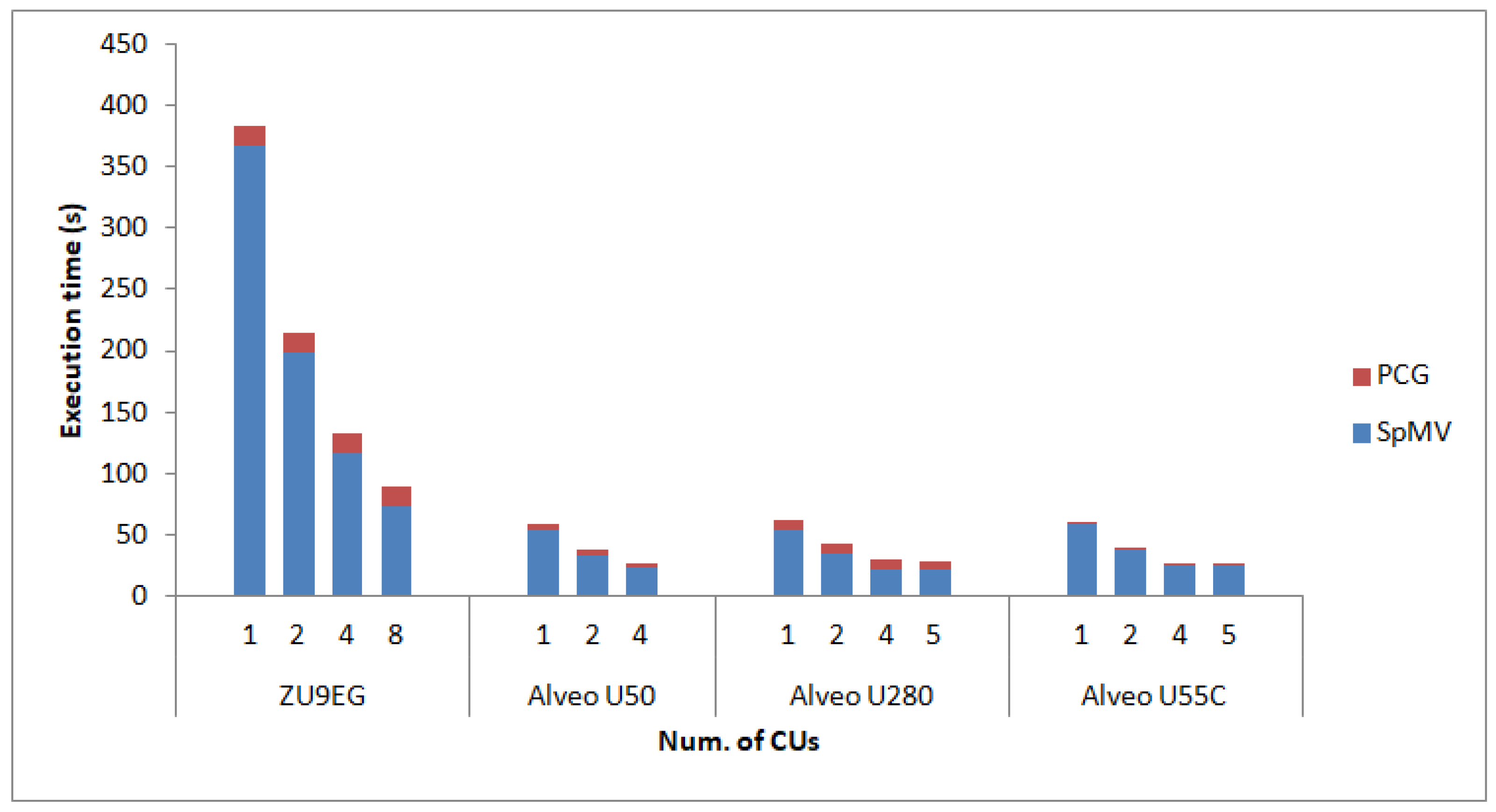
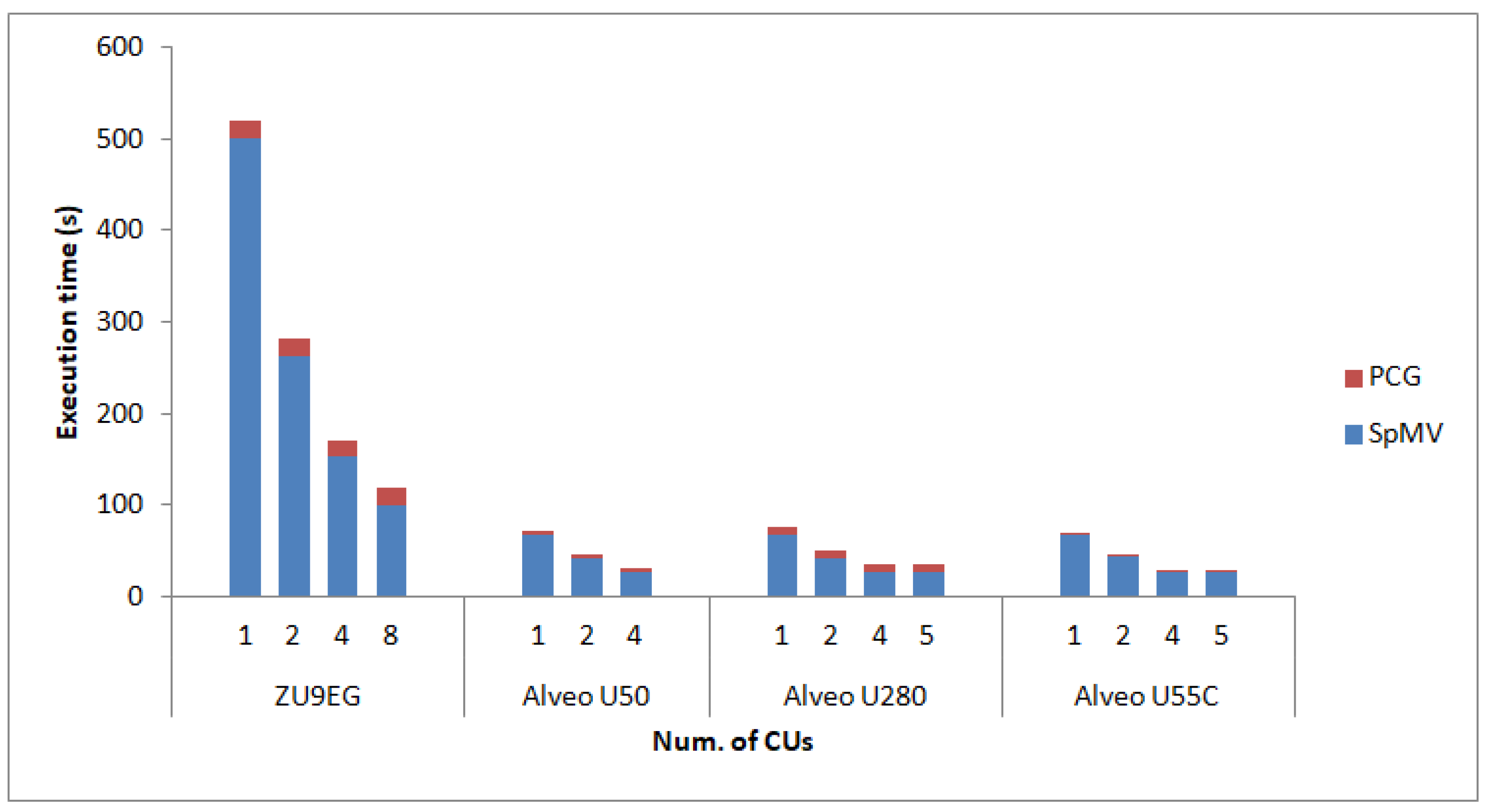
Hence,
Figure 2,
Figure 3 and
Figure 4 show the obtained results in terms of execution time for 100 iterations of the PCG; the cost of the SpMV products is highlighted in blue. The execution times presented include host software execution, the I/O from/to the FPGA fabric, and the execution of calculations within the FPGA. As expected, the execution time decreases significantly when multiple SpMV CUs are utilized for the calculation.
Moreover, PCG performance is closely dependent on that of the SpMV products, as these are the most time-consuming operation of the whole iterative scheme. Nevertheless, the increase in the number of SpMV CUs does not lead to a linear decrease in the execution time of the SpMV calculations as it should. The reason for this is that the x input vector and y output vector are shared between the SpMV CUs. In contrast to the A matrix, which is distributed among different buffers so that each CU can access its portion in parallel, the x and y vectors reside on the same buffer for all CUs. Distributing the x and y vectors is indeed possible, but x requires a copy of the whole vector for each CU, while y needs to be initially distributed to each CU, and then at the end of the SpMV operation to be merged back. Experiments showed that these two operations increase the execution time. The multiple copies of vector x and the distribution and merging of vector y is more expensive in execution time than the effect of the congestion on the shared memory ports.
Moving onto comparing the different FPGA-based setups, results show that the embedded-based ZU9EG is significantly slower than the Alveo accelerator cards that are coupled with powerful CPUs. This result is the combination of four factors. Firstly, the red portion of the execution time is affected by the low processing power of the ARM-A53 processor. Secondly, the accelerators are significantly slower as they operate at 150 MHz compared to the 300 MHz clock used on the Alveo cards. Thirdly, the vectorization for these accelerators on the Alveo cards allows eight double precision numbers to be read and processed simultaneously, as the memory interface supports 512 bit-wide interfaces. On the ZU9EG, only two double precision values fit into the 128 bit-wide interface between the FPGA and the processing system and the DDR memory. The SpMV execution time is affected only by the lower operating frequency, as it does not support vectorization. Finally, the utilization of HBM (460 GB/s) on the Alveo cards offers significantly higher memory bandwidths than the DDR memory (19 GB/s) of the ZU9EG.
With respect to the comparison among the different Alveo accelerator cards, we observed that the execution times measured are very similar. The architecture of the accelerators is almost the same between the three Alveo cards, with an exception being the number of CUs of the U50 (four CUs instead of five for the rest of the Alveo cards) and the slower dot accelerator on the U280. These two differences, along with the slower CPUs compared to those of the new U55C-based platform, justify the small decrease in performance.


 ,
, 


