1. Introduction
Impedance Spectroscopy is an instrumentation technique that measures the electrical complex impedance of a biological system when it is excited with different frequency voltage signals. Due to its electrical nature, the physiological behavior and state of a biological component directly affect its impedance. For this reason, a precise impedance measurement on a biological system gives us information on the internal physiological processes variations.
Impedance spectroscopy is a non-invasive, fast, low cost and portable technology. Due to these properties, it is a perfect technique to be applied in the industry to measure food quality and in healthcare and biomedical applications. The technique has been successfully applied in different studies. At food industry, it has been used for quality inspection on fruit [
1,
2], fish and meat [
3,
4], and beverages [
5,
6]. In healthcare and biomedical applications, it has been used in cardiography, cancer diagnosis, tissue analysis, and biosensing [
7,
8].
Adapting the technique to industrial environments is one of the current impedance spectroscopy challenges. To perform this, the technique should be fast, low-power, reliable, adaptable to detect different quality parameters on various foods, and easily upgradable to improve detection with new algorithms.
To achieve the above objectives, the present paper proposes using an FPGA as the main signal processor on the impedance spectroscopy instrumentation and AI algorithms at the edge to improve quality detection.
FPGA-based instrumentations have several notable properties. They are compact and portable, cross-platform compatible, have low latency, are reconfigurable, and allow edge processing and machine learning hardware acceleration. Therefore, FPGAs have been integrated into different research areas’ instrumentation equipment [
9]. Regarding Impedance Spectroscopy, FPGA-based systems can be found in different studies [
10,
11,
12,
13].
The typical FPGA-based impedance spectroscope is composed of an FPGA, one Data Acquisition Converter (DAC), an analog front-end, sensor probes, and two analog to digital converters (ADCs). The measurement process requires two stages: sample excitation and measurement. At the excitation process, the FPGA generates a signal that is converted into a voltage or current through the DAC and the analog front-end. This signal is applied to the sample through the sensor. In the measurement process, the sensor and the analog front-end measure a voltage and the current on the excited sample. These two measures are digitalized using the two ADCs. FPGA processes these signals to obtain the impedance phase and modulus. This process can be repeated several times using different frequency excitation signals. In the end, the system has impedance modulus and phase at the sample for different excitation frequencies.
Several FPGA-based impedance spectrometers are based in commercial data acquisition boards [
10,
14]. These boards are composed of one FPGA and several high-speed ADCs and DACs. FPGA configuration can be modified with custom-made hardware adapted to achieve the designed system performance specifications. These spectrometers are made up of the commercial board, together with a custom-made analog front-end and the sensor. The presented paper system is based on a commercial data acquisition board Red Pitaya STEMlab 125-14 [
15].
It is important to remark that a third process should be performed over the measured information, data analysis. Usually, data analysis is complex and performed outside of the instrumentation system [
16]. Several statistical methods such as principal component analysis, linear discriminant analysis, ANOVA, least-squares analysis, and several machine learning methods such as logistic regression, support vector machine, and K-nearest neighbors have been applied successfully to extract information from the measured data [
16]. Also, there are some works that have successfully applied data analysis based on Artificial Intelligence (AI) techniques [
13,
17].
Artificial Neural Networks (ANN) are efficient algorithms to classify and perform estimations over impedance spectrum measured data. It is a methodology that can be implemented in industrial FPGA-based instrumentation systems that require automated analysis [
18].
Applying data analysis and performing estimations and classification inside the measurement instrument without or reducing access to cloud services is known as edge computing. Using FPGA-based systems to perform AI edge computing has several advantages over other AI edge computing architectures such as the GPU based. These advantages include providing a throughput independent of the workload, achieving high performance for complex concurrent AI structures, and obtaining better energy efficiency than other non-FPGA-based architectures. On the other hand, developing hardware on FPGA-based edge AI systems is complex for most programmers [
19].
FPGA, traditionally, has been programmed using low-level “Hardware Description Languages” (HDL) such as VHDL or SystemVerilog. However, in the last few years, “High-Level Synthesis“ (HLS) tools have been developed and popularised. HLS tools convert behavioral C/C++ algorithms descriptions into low-level descriptions.
HLS tools infer parallelism from the sequential C/C++ described algorithms and exploit it to achieve higher throughput and low latency. Although you can directly convert any C/C++ program or software function into a synthesizable RTL code, this is not optimal. HLS tools provide different options and pragmas to drive the C/C++ code conversion into RTL description. Proper use of these HLS options and pragmas is essential to achieve an optimal hardware implementation in speed and area.
HLS tools focus designers on what they need to do instead of specifying how to implement it for a given reconfigurable hardware [
20]. These tools reduce the FPGA hardware developing time. Consequently, HLS described systems could be upgraded easily, improving their adaptability.
Using HLS descriptions to design the impedance FPGA-based spectrometer data analysis block is a proper solution to develop a system that can be easily upgraded with new algorithms to improve parameter detection over measured data. Considering ANN, these algorithms require several iterations to process the data. The operations applied to process the data are matrix multiplication or matrix-vector multiplication. The performed calculations involve applying several nested loops to the data.
The HLS compiler will only infer task-level parallelism from function calls. The sequential code blocks (such as loops) which need to be run concurrently in hardware should be put into dedicated functions. One of the desired objectives is to implement data processing algorithms, minimizing the FPGA used resources. To do this, a proper HLS description that divides operations into small functions simplifies path control and improves parallelism. Then, to achieve functions high performance, pipe techniques should be applied to the data loops. For this, using stream-based communication between functions allows consumers to start data processing as soon as producers start data generation, allowing overlapping the execution, which increases parallelism and throughput.
Therefore, using properly HLS as a description language reduces the time needed to implement a time and resource-efficient new ANN topology.
This paper presents an FPGA-based impedance spectrometer with edge AI data analysis using HLS described ANN. The system is based on a 7010 Zynq FPGA Red Pitaya board with custom FPGA firmware. The spectrometer has been developed to be used in the food industry to detect poultry breast anomalies using edge AI computing. The system is fast, low-power, reliable, and adaptable to detect different poultry breast anomalies. Authors have previous experience developing impedance spectrometer systems for poultry breast anomalies detection [
3,
21]. The presented system architecture is flexible and adaptable, allowing it to perform AI data analysis over impedance measured data on other food or healthcare applications. The developed system is a prototype that allows us to verify the feasibility of the technique in an industrial environment. In order to design a definitive system for an industrial environment, the security of the system should be improved to protect the system from potential threats. Using a zynq-based system allows us to perform these security tasks [
22].
The paper is organized as follows: This first section introduces the impedance spectroscopy technique and the drawbacks of adapting and improving the technique for industrial environments. The second section describes the FPGA system architecture. The section is divided into several subsections: Generation and acquisition system, FPGA data analysis, and processing engine ANN. The third section talks about the HLS code optimization applied to improve the system. The fourth section presents the obtained results and their comparison with other edge-AI FPGA-based systems. The last section presents our conclusions.
2. FPGA System Architecture
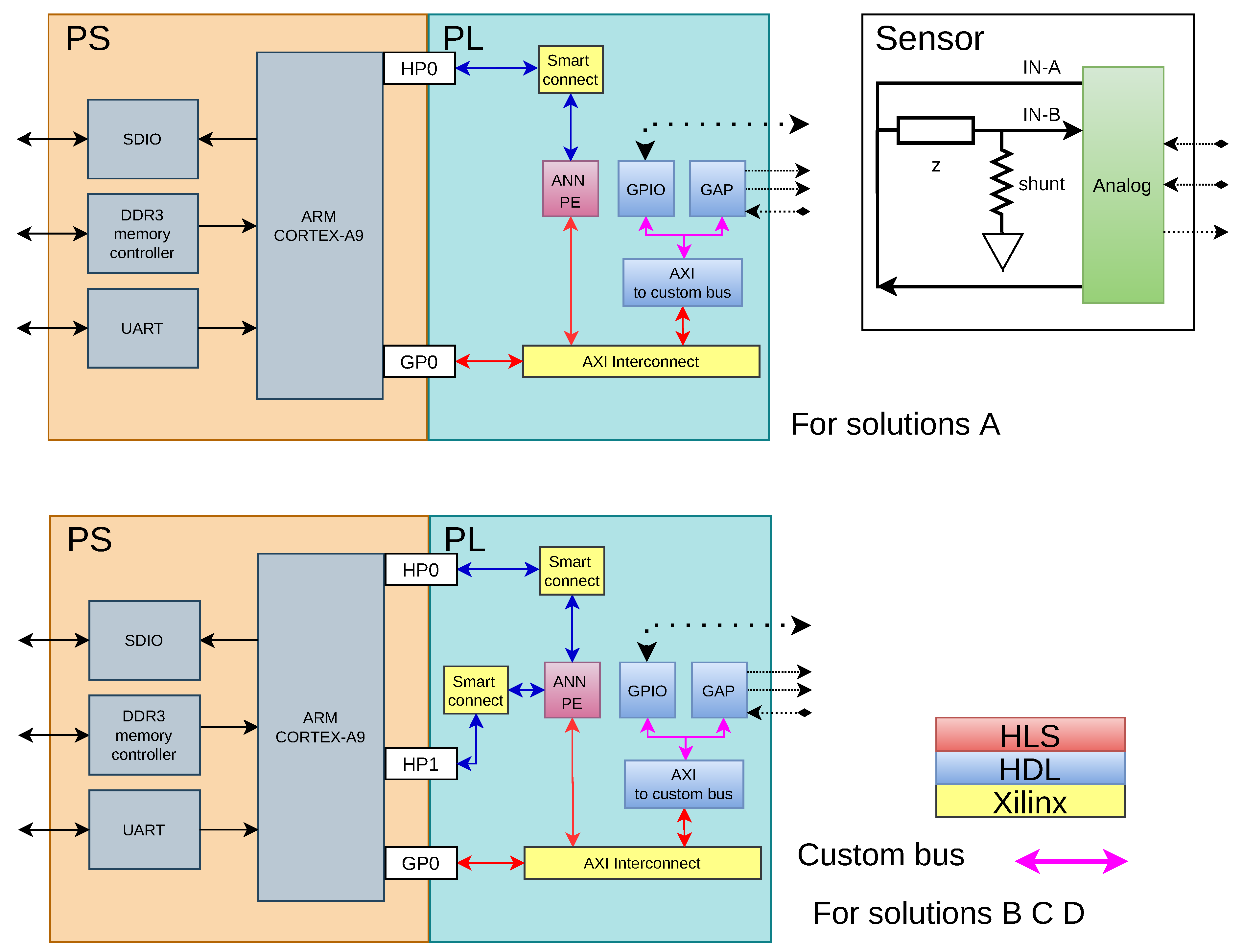
The system implemented on zynq 7010 red pitaya is presented in
Figure 1. The developed hardware is described in the PL (Programmable Logic) section, which is divided into two large blocks: the acquisition, processing, and generation section, with the module called GAP, and the analysis section that is performed by the module ANN PE. Two possible architectures to implement the system are presented. The architecture for solution A uses fewer resources compared to the architecture for the other solutions (B, C, D). This is a tradeoff between resources and processing speed.
It is important to remark that the ANN PE module allows us to carry out this type of configuration to gain processing speed.
GAP and ANN PE are described in more detail in the following sections.
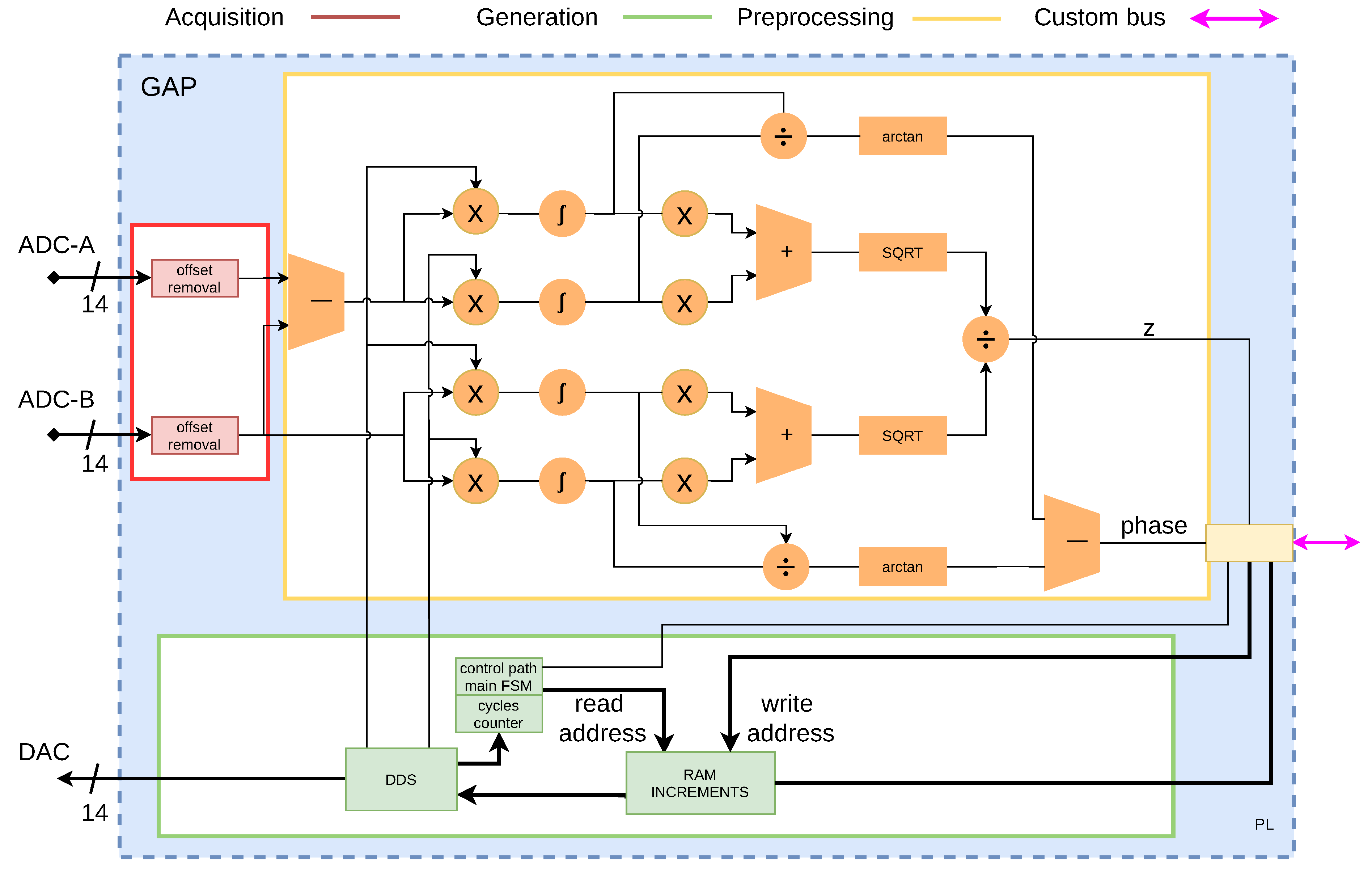
2.1. FPGA Generation, Acquisition and Preprocessing GAP
The application latency is a fundamental factor when AI at the edge is evaluated. In impedance spectroscopy, input signals have a marked sequential character that conditions the rest of the system (including the AI block) and determines much of the overall application latency.
Another remarkable feature of this type of application is that the acquisition trigger is generated by the application itself, either as a result of a user’s action or through the response of a pressure sensor that will indicate the right contact with the object of study. In any case, it derives in a start signal that will mark the beginning of the process that generates and acquires the ANN inputs.
The ANN inputs number can be obtained as the number of impedance spectra taken (in our application 4 spectra) times the number of frequencies in each spectrum sweep (in our case, 225 frequencies obtained performing a logarithmic interpolation between 40 Hz and 1 MHz) times the two obtained data for each frequency (impedance modulus and phase). Therefore, our neural network that must classify the studied object has an input layer of 1800 inputs (4 × 225 × 2). In our acquisition system, each frequency sweep lasts exactly 1130 ms so the two last ANN inputs from the 1800 total needed will be available 4.52 s after the acquisition begins.
As can be seen in
Figure 2, the ANN inputs generation, acquisition, and data preprocessing of block systems have been described at the hardware register transfer logic (RTL) level with HDL. The method used to calculate the impedance modulus and phase in the preprocessing block is the correlation method. The block is controlled by a Finite State Machine to decrease its latency below 5 s. Attempts to perform the generation, acquisition control, and preprocessing tasks using the FPGA embedded ARM microprocessor increased the signal acquisition times by an order of magnitude.
2.2. FPGA Data Analysis
In this section, the HLS developed ANN processing block components implemented in the FPGA are described. The presented architecture supports different ANN topologies (with a different number of layers and neurons per layer).
Type of Neural Networks
Different ANN topologies are available depending on the type of function they perform. The best known or used topologies are built by connecting different numbers of layers, with one input layer, N hidden layers, and one output layer. In the present work, Feed-Forward Neural Networks topology is used. Equation (
1) describes the computation for each neuron in different layers where
is the ANN number of layers
,
,
,
indicates the number of inputs for each layer, the input layer, the first hidden layer, the second hidden layer, and the output layer respectively. Indices
i,
j refer to different ANN neurons. Forwarding the data from left to the right, the neuron
j is located to the right of the neuron
i. The index
i represents the numbers of entries, where
…,
beginning with zero because it includes bias as input. The index
j represents the number of neurons in the layer
l, where
…,
. The
n index represents the
ANN input measured samples.
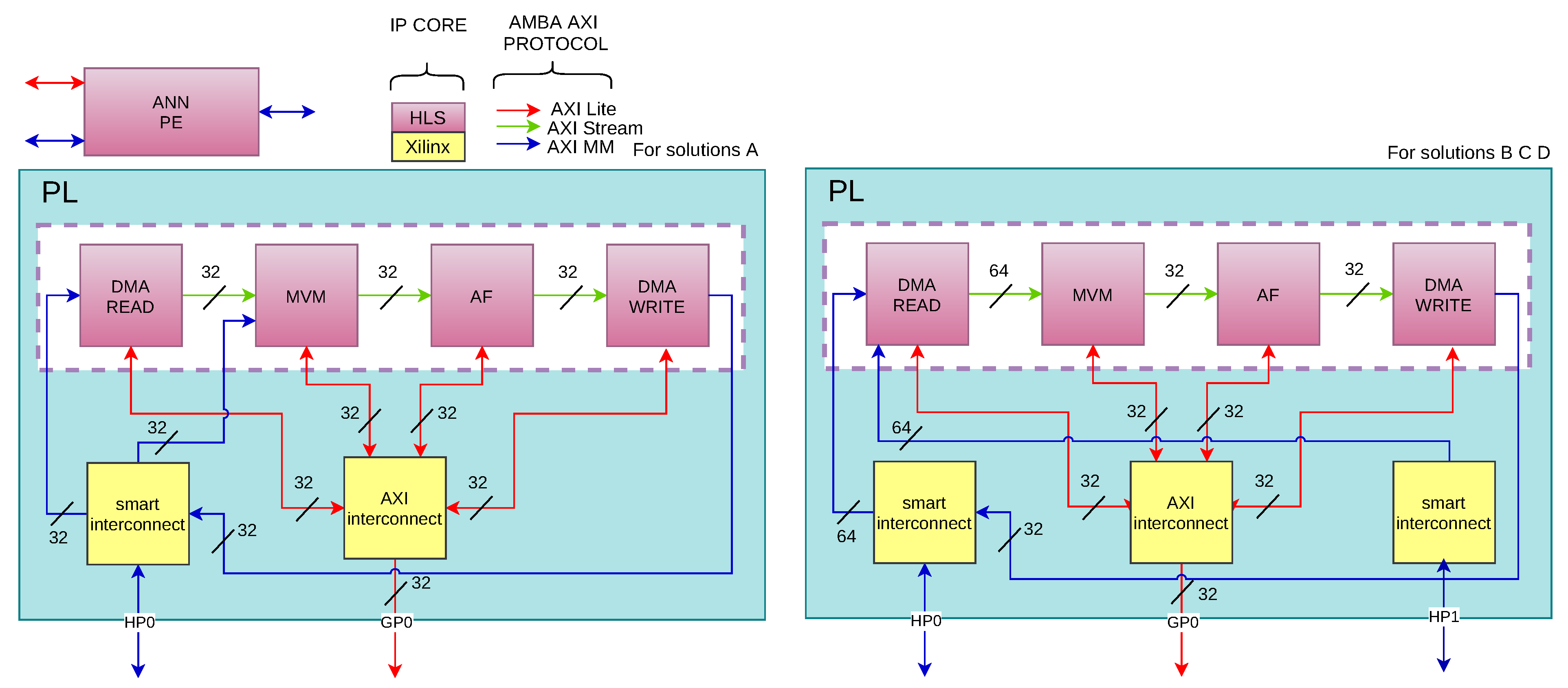
2.3. ANN Processing Engine
Based on the previous section’s described topology, our component is named “ANN Processing Engine” (ANN PE).
Figure 3 shows the integrated ANN PE with all the components needed to communicate with the microprocessor and DDR memory. The developed system uses the “Advanced Microcontroller Bus Architecture” (AMBA) protocols to interconnect the different system blocks: AXI-Lite protocol is used to configure each function, AXI-Memory Mapped Full protocol (AXI-MM Full) is used to transfer data between ANN PE and DDR memory, and AXI-STREAM is used to transfer data between internal functions in the ANN PE.
The ANN PE block has been divided into four HLS-developed blocks: DMA WRITE, DMA READ, Matrix-Vector Multiplication (MVM), and Activation Function (AF). DMA READ and DMA WRITE blocks have been developed to perform “Direct Memory Access” (DMA) to the DDR memory. DMA READ is for data reading, and DMA WRITE is for data writing. The reading DMA block uses the AXI-MM Full protocol to read from DDR the raw samples that the GAP section has previously stored in it and to read the ANN weights that are also stored in the DDR. The writing DMA block uses the AXI-MM Full to store ANN PE obtained results in the DDR memory.
The output data from the DMA read function is a stream in fixed-point or floating-point format, depending on the implemented solution.
The read samples and the ANN weights are received by the “Matrix-Vector Multiplication” (MVM) block through the AXI-MM protocol. MVM block should be configured with the number of neurons to be processed before starting the calculation. After MVM configuration, the calculation process begins when there is valid data in the AXI-STREAM input. When a neuron computation is completed, the result is propagated using an AXI-STREAM protocol to be processed by the “Activation Function” (AF). AF block is implemented using a look-up table. Finally, the DMA WRITE block writes the results of the current layer in DDR memory.
This process is repeated for each layer using the previous layer’s results as input. The last layer DDR stored results are the ANN analyzed impedance spectra measured data.
The following section presents the different HLS optimizations carried out in the present work. These optimizations allow us to have a fast, efficient, and reconfigurable data analysis system.
3. Optimization and Improvements
Working with FPGA, different levels of hardware optimizations are possible. HLS allows optimizations through its pragmas for performance, latency, area, throughput and interfaces.
The first ANN PE IP Core performed optimization level has been applied at the AXI-STREAM protocol communication between blocks. This optimization allows having a Producer-Consumer architecture. That is, when the producer function delivers an output result, immediately, the consumer function starts to operate with it. “First Input First Output” (FIFO) is applied between each function. The advantage of applying FIFO queues when AXI-STREAM is used is that each function’s control path is reduced in complexity.
Another optimization level applied is to select the right word size for the matrix-vector multiplication operations. 32-bit fixed-point words with I = 8 and W = 32 have been selected. This word size allows us to perform a DMA memory word read in each clock cycle. With this fixed-point word configuration in the MVM operation, it is possible to have a error compared to performing the same operations using a 32-bit floating point.
The developed read and write DMA functions have been optimized for high throughput and low initialization latency. As is described at the read DMA Algorithm 1 pseudocode, the implementation has been separated into two functions. The main function contains the AXI-MM and AXI-STREAM interfaces. The secondary function is responsible for converting from AXI-MM to AXI-STREAM at the read DMA function and for converting AXI-STREAM to AXI-MM at the write DMA function. If the pragma HLS DATAFLOW (that optimizes throughput and latency) is not applied, the secondary function generates an “Interval Latency” (IL) greater than 2. On the other hand, when the DATAFLOW pragma is applied, it is possible to reduce the IL to 2 clock cycles. In addition, as it is described in previous paragraphs, DMAs can read or write one 32-bit word per clock cycle respectively for solution A or 64-bit for solutions B, C, and D.
Considering the MVM function, different optimizations have been applied. The first decision was to store the weights in FPGA embedded memory. This allows for faster data processing, although it has the drawback that, due to the reduced memory space in FPGA, only ANN structures with small layers can be implemented. The other drawback is the time consumed sending and saving the weights to the Block-RAM (BRAM) memory. Consequently, a second optimization was implemented: remove the BRAM memories and add AXI-MM Full port to read the weights in a similar way to how the read DMA function executes reads from DDR memory. Although, in this optimization, the ANN weights reading begins when the first valid data is present at the input of the MVM AXI-STREAM interface, the cycles latency before the beginning of multiplications and sums calculation is increased, reducing the performance of the MVM function.
The last implemented MVM optimization starts reading the memory weights just before having the first Tvalid signal activation in the AXI-STREAM input data interface. In addition, a single for loop is used together with three pragmas that are applied to this loop. The first implemented pragma is PIPELINE with “Initialization Interval” . This allows the execution of the operation concurrently. Also, the ARRAY PARTITION pragma is applied to divide the samples vector and store it in individual registers without using BRAM. This improves the IP Core throughput. HLS has different pragmas to allocate resources for the executed operations. The low-resource FPGA device used has DSP cores that can perform multiplication and accumulation in one clock cycle. Applying the BIND_OP impl = DSP pragma forces DSP blocks to be used. The MVM implementation has been performed in a function, as described in the Algorithm 2 pseudocode. The sigmoid “Activation Function” (AF) has been implemented with a look-up table which generates one clock cycle latency.
HLS allows defining the IP Core control via hardware or software. By default, Vitis HLS generates several control signals to perform a Hardware IP Core control. To control via software the IP Cores, pragma HLS INTERFACE AXI-LITE port = return is applied to the ports grouped into s_axilite interface. The reason for using a software control is that the processing unit could be reusable to process different neural network layers. This allows us to control via software each of the functions individually.
The sequence of how the data flows from each function is shown in
Figure 4, where an example of a 3 inputs layer and 5 neurons is shown. The diagram shows how the AXI-STREAM and AXI-MM signals interact between the functions. It also shows the MVM function latency when a vector multiplied by a column of the weight matrix is computed.
| Algorithm 1 READ DMA |
- 1:
MMToStream - 2:
- 3:
- 4:
#pragma DATAFLOW - 5:
- 6:
fortodo - 7:
- 8:
- 9:
end for - 10:
dmaRead - 11:
- 12:
- 13:
#pragma INTERFACE AXI-Stream strmOut - 14:
#pragma INTERFACE AXI-Lite dataIn - 15:
#pragma INTERFACE AXI-Lite NWords - 16:
#pragma INTERFACE AXI-Lite control - 17:
MMToStream - 18:
- 19:
|
| Algorithm 2 Multiplication Vector Matrix |
- 1:
MVM - 2:
- 3:
- 4:
- 5:
- 6:
#pragma INTERFACE AXI-Stream strmOut - 7:
#pragma INTERFACE AXI-Stream strmIn - 8:
#pragma INTERFACE AXI-MM WInDDR - 9:
#pragma INTERFACE AXI-Lite rowsW - 10:
#pragma INTERFACE AXI-Lite control - 11:
inA, outC - 12:
P, Weight, tmp - 13:
IndexRW, IndexCP - 14:
inputBuf - 15:
- 16:
fortodo - 17:
#pragma PIPELINE II = 1 - 18:
#pragma ARRAY PARTITION inputBuf //Solutions A, B, C - 19:
#pragma ARRAY PARTITION inputBuf factor=2 cyclic//Solution D - 20:
- 21:
if then - 22:
- 23:
- 24:
- 25:
else - 26:
- 27:
- 28:
end if - 29:
- 30:
#pragma BIND_OP impl=dsp - 31:
- 32:
if then - 33:
- 34:
- 35:
- 36:
- 37:
else - 38:
- 39:
end if - 40:
end for
|
4. Results
Performance Evaluation
In AI at the edge applications, system latency and, derivatively, application throughput are often some of the most requested performance metrics.
Since most of the works are focused on computer vision applications, it is not surprising that frames per second (FPS) are widely used in different publications as the throughput measurement. This measure has been used in the present work to compare our results with other works; but it is essential to keep in mind that it is a measurement parameter very dependent on the network topology, which includes the input layer that would have the size of the starting image.
It is more interesting and independent of the topology to calculate the throughput as a function of the number of network parameters (mega parameters) calculated per second (Mps), remarking that it is generally understood that each synaptic connection involves one parameter (one Multiply-Accumulate operation which we refer to as MAC).
However, it should be noted that results using these throughput metrics are often masked by the programmable device architecture characteristics (granularity, number of variables per LUTs, and DSPs characteristics) and, fundamentally, by resources available and used in the chosen FPGA. To avoid this drawback, in the present paper, our solution’s computational efficiency goodness is measured as network parameters per second per DSP (which corresponds to a MAC operation in almost all manufacturer’s FPGA families).
Energy efficiency is also very important when AI at the edge processing is performed in limited battery capacity embedded devices [
23]. Energy efficiency is often reported as the number of operations per joule; but, in this work, mW/Mps, which means energy per operation, is used.
Finally, it is necessary to include two last aspects that our implementation perfectly fulfills and that cannot be ignored: flexibility and architectural adaptation. Some other implementations are unbeatable at the previous metrics, but at the cost of hardware time compilation for these specifically implemented topologies. This means that any topology change requires time-consuming hardware recompilation. And some implementations with dependency on group size (such as the NDrange kernel-based OpenCL implementations), even if they do not require recompilation, have an efficiency very dependent on the exact size of the layers.
The results are summarized in four tables.
Table 1 and
Table 2 show the different iterations performed to reduce FPGA resources and processing time to the ones needed in our application.
In the first solution, weights are loaded through the AXI-LITE protocol in BRAM memory instantiated in the MVM function. This implementation took up a large number of resources, and it was not feasible to add the other GAP section components. This implementation would be possible for small ANN topology sizes but is not reusable for bigger ANN topologies. Also, this solution has a latency due to the BRAM memory weights load process.
In the second solution, the MVM function reduced the BRAM memory needed because the weights were read from the DDR memory. However, the FPS that are processed is reduced, compared with the previous implementation. Here, at the same time that the DMA begins to read the sample vector and has a latency cycle to start pulling through its axi-stream output, the MVM function reads the weights from memory one by one generating a block with the input data.
The third iteration has been described in detail in the previous sections. It is important to emphasize that this solution can be integrated into the 7010 Zynq FPGA devices (see
Table 3), which are the lowest cost Zynq solutions (less than 400 euros). For example, our first iteration, which is the one that has the best results from a speed point of view (550 fps), requires a 7020 Zynq FPGA family device, the cost of which is twice the previous one. Also, a floating-point version, which uses more FPGA resources than the fixed-point version, can be integrated into the 7010 devices, as can been seen in
Table 4.
Although in the third solution the speed performance is slightly lower than the first one, it has better energy and computational efficiencies than those shown in the most recent publications (see
Table 2).
The scalable accelerator for large-scale DL networks DALU by Wang et al. [
26] references 3 topologies (784-64-64-10, 784-128-128-10, and 784-256-256-10) on a 7020 ZYNQ FPGA. Their work presents a poor energy efficiency (69.93 mW/Mps) but, comparatively, it can be considered a low power (234 mW) solution.
The work detailed in [
24] proposes an SSAE optimized at the RTL level to achieve the best system performance in terms of throughput and energy efficiency. However, to achieve this performance, they use 12-bit fixed data types that provide lower accuracy (93.3%). The low computational efficiency achieved is the problem with this solution.
Undoubtedly, Belabed et al. [
25] is the best solution for the referenced studies in the present paper. Their solution achieves a throughput that stands out above all. A very high number of DSPs have been used to obtain these results. That makes its computational efficiency inferior to our third implemented solution. Their solution cannot be implemented on a 7010 Zynq device, as can be seen in
Table 4.


 ,
, 


