Communication

A New Approach to Power Distribution by a Dual-Gate MOSFET for Controlling a Smart Actuator Array

1
Department of Electrical Engineering, Inha University, Incheon 22212, Korea
2
Department of Mechanical Engineering, Inha University, Incheon 22212, Korea
*
Author to whom correspondence should be addressed.
Electronics 2022, 11(18), 2956; https://doi.org/10.3390/electronics11182956
Submission received: 23 August 2022 / Revised: 6 September 2022 / Accepted: 16 September 2022 / Published: 18 September 2022
(This article belongs to the Special Issue Power Electronics Converter Topologies and Control Techniques)

Abstract

:
Remotely driven smart actuator technology by microwave is attractive since it simplifies and reduces the complexity and weight of the remote system. A rectifying antenna (rectenna) array receives and converts microwave power into DC power for actuators, and the power collected from the rectenna array should be accurately allocated and distributed to each actuator. In this research, a new power distribution (PD) logic circuit is studied to control an actuator array effectively. The PD logic circuit was designed and tested to validate it. The preliminary design was tested for a 4 × 4 piezoelectric actuator array with a 16 dual-gate MOSFET array and a computer-controlled 16-channel DAC board. Additionally, power compensation as a remedial approach for a partial power failure of the array was integrated. This PD scheme with a new logic device simplifies the thousands of control cables required for connecting each array element. The performance and limitations of the designed PD circuit are discussed.

1. Introduction

Smart actuators or smart material actuators that can change shapes for a designed intention are used for large and flexible structures [1,2]. Large flexible and deployable membrane structures must possess surface error correction and self-configurable functions to perform their mission. Surface error control of large flexible membrane structures is challenging, which requires segmentation of the wiring system in an array matrix. This surface control is critical to succeeding in space missions [3,4,5,6,7], including large aperture space telescopes that will advance and drastically enhance the deep space search operation for expanded exploration capability.
The microwave-powered smart actuator concept [8,9,10,11,12,13,14] has gained attention for the wireless operation of actuator arrays for large, ultra-lightweight smart structures. A rectifying antenna, a so-called rectenna, can convert microwaves into DC power and deliver power wirelessly. However, there is limited information about distributing power for individual actuators, allowing various shape changes without the complex wired circuitry network and associated weight.
A power distribution (PD) logic circuit was devised to alleviate a complex wire network that might consist of thousands of wire connections. The role of the PD logic circuit is mainly managing power for effective use by a logic decision algorithm that allocates the power to the actuator array where the shape change must be performed. The Schottky barrier diode’s breakdown voltage determines each rectenna’s maximum operating voltage [11,13,15]. Accordingly, the maximum voltage of the rectenna array is not enough for smart actuators. On the other hand, the power obtained from a single rectenna may not be enough for feeding a single actuator since the dispersive nature of microwaves results in a low power density, and it cannot meet the power requirement for shape changes. Low power flux density is typical for long-distance transmitted microwaves. High-energy and high-frequency microwave sources must have low dispersive power transmission for a high flux density, but the currently available systems are bulky and heavy. The issues associated with microwaves’ low power density or high power requirement for applications can be mitigated using a PD circuit concept.
A hard-wired control circuit could work appropriately only for a system with a few actuators. Suppose a system has many control nodes that require power supplies and controls; then, wiring may not be a practical solution due to the sophisticated power gate switching and control networks, the wired network’s weight, and the power and control schemes’ dependency. The shape control of many nodes for deployable antennas or aerospace morphing structures is challenging when developing control networks. Onboard control and power networks bring complexity to wiring and power systems.
This paper reports a new concept of PD logic circuits to effectively control a rectenna/actuator array. The PD logic circuit was designed and evaluated to investigate the validity of the power distribution and the response time. A network circuitry interconnecting the control feature of all participants distributes power to actuator groups from one to other locations. The networked power allocation is also a power amplification process to the actuator group’s power requirements. The power fed to the actuator group is allocated to each element according to power needs. The number of row or column wires is required for two times the square root of the actuator numbers. A typical network of an N power grid requires N2 wire interconnections for power management, but the PD logic circuit based on a dual-gate metal-oxide-semiconductor field-effect transistor (MOSFET) needs merely 2xN wire interconnections. Table 1 compares the proposed PD circuit and conventional hard-wired PD systems.

2. PD Circuit Design and Experiment

2.1. PD Logic Design

The PD logic routine considered for actuator array operation is shown in Figure 1. A 4 × 4 actuator array is shown, for example, and 4 × 4 dual-gate MOSFETs are arrayed. The diagram of PD logic is analogous to power grid lines crisscrossing in a connected grid. The first element of the circuit is constructing a power lattice or grid layer. The PD logic routine has vertical lines–columns and horizontal lines–rows. They are electrically conductive lines. Actuators are connected at the nodes of the crossed vertical and horizontal lines on the actuator layer. Four directions distribute the power to each actuator. Such a power feed scheme ensures power is delivered to a given node, even when other cross-links are broken. Once at least one line is alive, power can be fed into the actuator. Even if all four directions are broken, power could be delivered, controlling all other nodes in the actuator array.
The most important component in the PD circuit is possibly a variable resistor. A dual-gate MOSFET functions as a variable resistor [16,17]. Thus, dual-gate MOSFETs were adopted for the PD logic circuit. Enhanced-power MOSFETs are classified as voltage control devices because the gate-to-source voltage, VGS, controls the current drain, ID. When the VGS is large, near 10 volts, the source-to-drain resistance diminishes to a small value, lower than 1 ohm. The current drain, ID, is decided by the load’s impedance and the drain voltage’s magnitude. A low voltage application to the source to the gate, for example, 0 volts, increases the source-to-drain resistance up to megaohms, turning off the MOSFET. Thus, a MOSFET can function as a control component to a designated actuator element.

2.2. Control of MOSFETs

The next sequence is how to address or control each MOSFET. The same principle of the control scheme used for refreshing DRAM can be adopted. The voltage of memory logic is memorized in a capacitor of the memory. The capacitor needs a refresh periodically to maintain the memory. Rows and columns are charged systematically to refresh the memory.
Similarly, nodes in the PD circuit can be addressed by applying a high voltage to the corresponding column and row. This sequence indicates that the MOSFET can be turned off independently using two gate inputs of a dual-gate MOSFET. The MOSFET will only conduct in a true AND gate manner when column and row inputs (both gates) are high. Most MOSFET components used now are single-gate ones. In the early days, dual-gate MOSFETs were manufactured for VHF amplifiers and mixers. Motorola dual-gate depletion-mode MOSFETs (MFE201) were used in this work. The depletion-mode operation of the MOSFET requests from the PD circuit a negative gate voltage to turn off the MOSFET.

2.3. Circuit Fabrication

Figure 2 shows the 4 × 4 PD circuit system arrayed with 16 MOSFETs on a breadboard. The G2 gates of four MOSFETs were connected in every row. A row activation signal was given to all G2 gates in the first row to activate the first row (see row 1 in Figure 1). In addition, all G1 gates of the first MOSFETs in each row were tied together to form the first column (column 1 in Figure 1). A varying value of voltage can be given to each column to activate each actuator in the row to maintain the ON condition. It results in two electrically independent layers in the PD circuit. All the G2 gates were connected in four rows to form the first layer, and the second layer was formed by tying all the G1 gates in four columns. Four-row wires (rows 1–4 in Figure 1) and four-column wires (columns 1–4 in Figure 1) were constructed to control 16 MOSFETs with the related actuators.
Finally, a 16-channel digital-to-analog converter (DAC) was used in a personal computer to turn on and off the rows and columns of the PD circuit in a round-robin manner. An analog channel was utilized for each row or column separately. The DAC output board was controlled using a Visual Basic program. Figure 3a displays the control panel of 16 actuators generated by the Visual Basic program. First, channel 8 of the DAC board switches from −5 (off) to 0 volts (on). As it is connected to all G2 gates in the first row of actuators, row 1 becomes active. Figure 1 shows the arrangement of rows and columns. After that, channels 1 to 4 of the DAC are set to the targeted voltages for the actuators (1,1) to (1,4). Voltages for the actuators can be set independently because each channel is connected to a separate G1 gate in row 1. Channels 1 to 4 are turned off sequentially, and finally, channel 8 is turned off. The actuators in row 1 are activated to the targeted voltages. Figure 3b shows an example of a sequentially decreased output voltage.
Next, channel 9 of the DAC is switched from −5 to 0 volts. As all the G2 gates are connected in the second row, it turns row 2 active. Channels 1 to 4 are assigned to the targeted voltage for actuators (2,1) to (2,4). The targeted voltages can be given independently since channels 1 to 4 are connected to separate G1 gates in row 3. Following this, channels 1 to 4 are turned off sequentially, and finally, channel 9 is turned off. The actuators in row 2 are now assigned to the targeted voltage level. The order of the sequence ends with channels 10 and 11. The program comes back to channel 8 and row 1 as all sixteen actuators are activated.

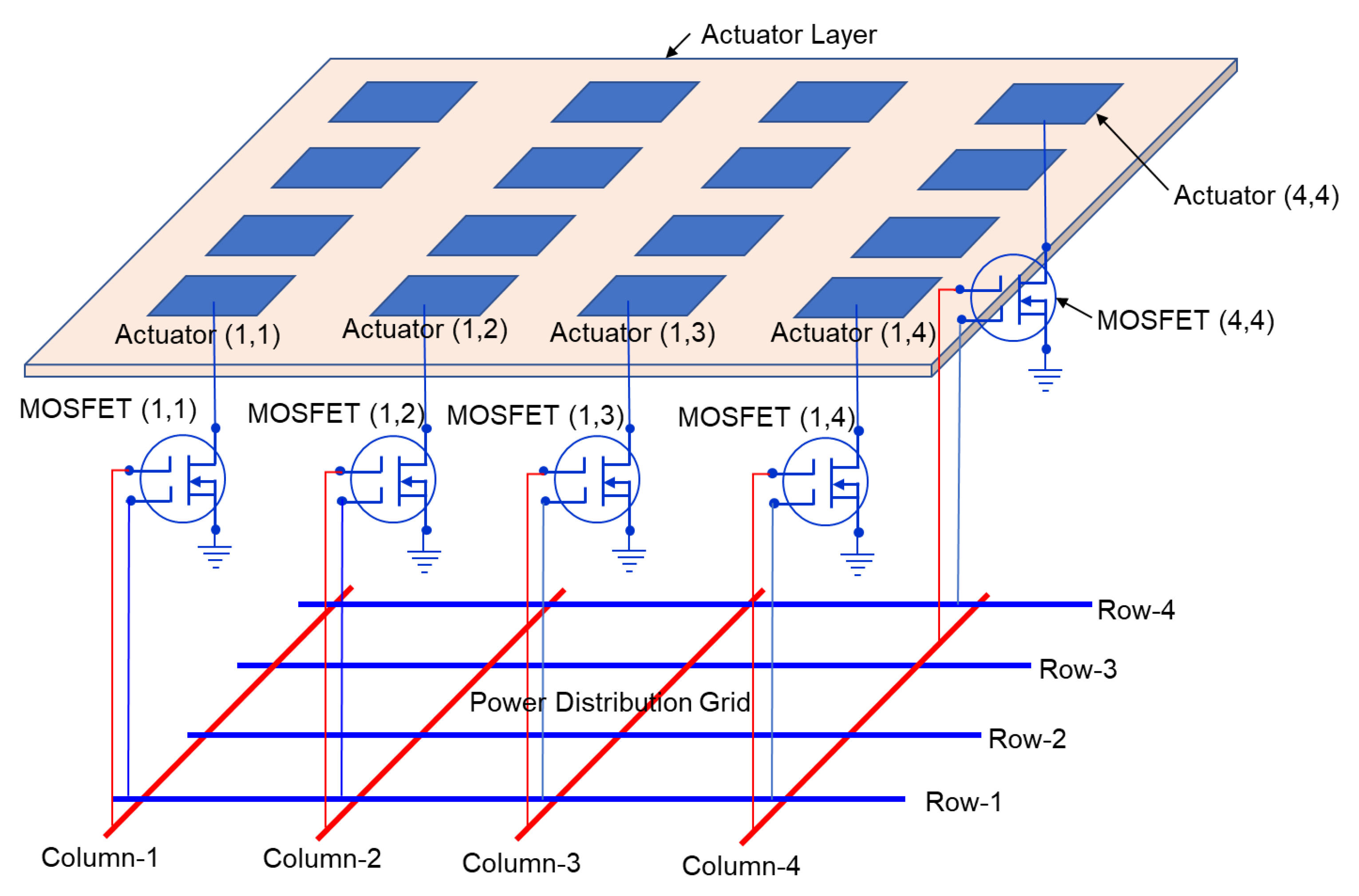
2.4. PD Circuit and Piezoelectric Actuators

A stacked piezoelectric actuator with an amplification mechanism (APA400M, Cedrat Technologies) was used in this research, as shown in Figure 4 [18]. It has a maximum displacement of 460 µm at 150 volts. The piezoelectric actuator has a wide actuation voltage range from −20 to −150 volts. Piezoelectric actuators are voltage-controlled devices representing an equivalent circuit of a capacitor and resistors. The capacitance value dominates the equivalent circuit. Thus, the designed PD circuit can be tested by emulating the piezoelectric actuator with a capacitor representing the piezoelectric actuator under a pulse charging for a short cycle. Once the actuator has a low leakage level, it will maintain that voltage until the next pulse recharges it. The actuator cannot dissipate the charge when it does not have sufficient leakage. In that case, a resistor is necessary across the capacitor to emulate the accumulated charge dissipation of the piezoelectric actuator. A 1.5 μF epoxy-dipped tantalum capacitor was chosen to emulate the actuator for our test. Typical capacitors have micro-amps-range leakage under 10 volts, equivalent to the internal resistance of 5 to 10 megaohms at the capacitor. The time constant determined by the embedded RC circuit is approximately 7.5 s.

3. Results and Discussion

3.1. PD Circuit Test

Since depletion-mode dual-gate MOSFETs were used, negative voltages were applied to control the MOSFETS in the PD circuit. The analog output board was able to supply negative and positive voltages. The MOSFET was turned off with −5 volts on G1 and G2, and when 10 volts was applied across the 1.5 μF capacitor in the PD circuit, 15 milli-volts was noticed. This voltage might be due to the leakage current going through the capacitor and the MOSFET leakage. After a couple of minutes, the leakage voltage dropped to 6 or 7 milli-volts. A good-quality MOSFET may mitigate the leakage to an acceptable level. Since piezoelectric actuators require a high voltage of more than 100 volts, less than 1-volt leakage could be an acceptable level. Nonetheless, when we tested the piezoelectric actuator with the PD circuit, the output result did not indicate significant power leakage influence because the resistance of the piezoelectric actuator could mitigate the current leakage.
Figure 5a shows the average output voltage to 16 (4 × 4) actuators. The voltage for one actuator was 10 volts. Distributing the power to two actuators from a 10-volt input resulted in 5.0 volts for each actuator. Similarly, the power distributing process continued up to 16 actuators, and the average output voltage decreased as the number of actuators increased. Since the signal-to-noise ratio for the measurement is about a million to one, the output result does not exhibit significant power leakage. Figure 5b represents the average power output from the 16 actuators. The average output power per actuator increases as the number of actuators increases. The mean value of the average output power per actuator is 0.21 μwatts. It might be due to voltage drifting with time associated with the thermal noise effect of the circuit.
The thin film microcircuit embodiment of the PD circuit provides membrane flexibility, a small size, and a light weight for space applications. A thin film PD circuit can be embedded into a single embodiment with a rectenna or actuator array. However, a high-voltage dual-gate MOSFET must be fabricated in the thin film PD circuit.

3.2. Piezoelectric Actuator Test

For demonstration purposes, this circuit test showed the successful operation of piezoelectric actuators. The actuators performed approximately 460 μm displacement from the test by applying the 150-volt level to MOSFET devices. Note that the piezoelectric actuator can produce 300 m displacement under 100 volts, which could be enough for compensating the surface errors of a deployable reflector antenna. In the PD circuit design, however, 100 driving voltage could be the maximum stable value for the actuators. A truly high-voltage dual-gate MOSFET PD circuit may need to be designed for high-voltage piezoelectric actuators.

4. Conclusions

The conceptual design of the PD logic circuit was presented, and its feasibility was demonstrated for smart actuators. The proposed PD circuit is a realistic and reasonable solution to avoid or alleviate the network complexity of powering smart actuators. An example of a 4 × 4 array PD circuit for piezoelectric actuators was experimentally tested. The test results show that piezoelectric actuators, which require a relatively low driving voltage, can be utilized by the PD circuit with a large degree of controllability. The PD logic circuit’s layout presented here is compact and simple enough to be miniaturized into a microcircuit platform by embedding the PD logic circuit directly into the smart actuator array. The dual-gate MOSFET gives a unique response and controllability in the PD circuit. A thin film PD circuit can be embedded into a single embodiment with a rectenna and actuator arrays. The thin film microcircuit embedded in the PD circuit can provide membrane flexibility, a small size, and lightweight behavior essential for space structural applications.

Author Contributions

Conceptualization, J.K.; methodology, S.-H.L. and J.K.; software, S.-H.L.; validation, J.K.; formal analysis, J.K.; investigation, S.-H.L.; data curation, S.-H.L.; writing—original draft preparation, J.K.; writing—review and editing, S.-H.L. and J.K.; visualization, S.-H.L.; funding acquisition, S.-H.L. All authors have read and agreed to the published version of the manuscript.

Funding

This work was supported by an Inha University Research Grant.

Acknowledgments

This work was supported by an Inha University Research Grant.

Conflicts of Interest

The authors declare no conflict of interest.

References

  1. Kim, J.; Kim, J.W.; Kim, H.C.; Zhai, L.; Ko, H.U.; Muthoka, R.M. Review of Soft Actuator Materials. Int. J. Precis. Eng. Manufactur. 2019, 20, 2221–2241. [Google Scholar] [CrossRef]
  2. Bahl, S.; Nagar, H.; Singh, I.; Sehgal, S. Smart materials types, properties and applications: A review. Mater. Today Proceed. 2020, 28, 1302–1306. [Google Scholar] [CrossRef]
  3. Liu, Z.Q.; Qiu, H.; Li, X.; Yang, S.L. Review of Large Spacecraft Deployable Membrane Antenna Structures. Chin. J. Mech. Eng. 2017, 30, 1447–1459. [Google Scholar] [CrossRef]
  4. Kim, H.J.; Hariharan, S.; Julian, M.; MacDonnell, D.G. Technology and opportunities of photon sieve CubeSat with deployable optical membrane. Aerosp. Sci. Technol. 2018, 80, 212–220. [Google Scholar] [CrossRef]
  5. National Aeronautics and Space Administration, SRTM Mission Statistics. Available online: https://www2.jpl.nasa.gov/srtm/statistics.html (accessed on 28 April 2021).
  6. Schenk, M.; Viquerat, A.D.; Seffen, K.A.; Guest, S.D. Review of Inflatable Booms for Deployable Space Structures: Packing and Rigidization. J. Spacecr. Rocket. 2014, 51, 762–778. [Google Scholar] [CrossRef]
  7. Mughees, M.; Sadaf, M.; Gelani, H.E.; Bilal, A.; Saeed, F.; Chowdhury, S.; Techato, K.; Channumsin, S.; Ullah, N. Comparison of Efficiency-Based Optimal Load Distribution for Modular SSTs with Biologically Inspired Optimization Algorithms. Electronics 2022, 11, 1988. [Google Scholar] [CrossRef]
  8. Wagih, M.; Weddell, A.S.; Beeby, S.P. Rectennas for RF Energy Harvesting and Wireless Power Transfer: A Review of Antenna Design. IEEE Antennas Prop. Mag. 2019, 62, 95–107. [Google Scholar] [CrossRef]
  9. Yang, S.Y.; Kim, J.; Song, K.D. Flexible patch rectennas for wireless actuation of cellulose electro-active paper actuator. J. Electr. Electronic Technol. 2012, 7, 954–958. [Google Scholar] [CrossRef]
  10. Song, K.D.; Kim, J.; Kim, J.W.; Park, Y.; Ely, J.J.; Kim, H.J.; Choi, S.H. Preliminary operational aspects of microwave-powered airship drone. Int. J. Micro Air Vehicles 2019, 11, 1–10. [Google Scholar] [CrossRef]
  11. Choi, S.H.; Song, K.D.; Golembiewski, W.; Chu, S.-H.; King, G.C. Microwave power for smart material actuators. Smart Mater. Struct. 2004, 13, 38–48. [Google Scholar] [CrossRef]
  12. Yang, S.Y.; Mahadeva, S.K.; Kim, J. Remotely powered and controlled EAPap actuator by amplitude modulated microwaves. Smart Mater. Struct. 2013, 22, 017001. [Google Scholar] [CrossRef]
  13. Yang, S.Y.; Kim, J. Wireless power transmission using dipole rectennas made on flexible cellulose membrane. IET Microw. Anten. Prop. 2012, 6, 756–760. [Google Scholar] [CrossRef]
  14. Song, K.D.; Yi, W.J.; Chu, S.H.; Choi, S.H. Microwave Driven THUNDER Materials. Microw. Opt. Technol. Lett. 2003, 36, 331–333. [Google Scholar] [CrossRef]
  15. Yin, J.; Chen, S.; Chen, H.; Li, S.; Fu, H.; Liu, C. Design Space of GaN Vertical Trench Junction Barrier Schottky Diodes: Comprehensive Study and Analytical Modeling. Electronics 2022, 11, 1972. [Google Scholar] [CrossRef]
  16. Yoon, Y.J.; Lee, J.S.; Kim, D.; Lee, J.; Kang, I.M. Gallium Nitride Normally Off MOSFET Using Dual-Metal-Gate Structure for the Improvement in Current Drivability. Electronics 2020, 9, 1402. [Google Scholar] [CrossRef]
  17. Choi, S.H.; Song, K.D.; King, G.C.; Woodall, C. Rectenna Performance for Smart Membrane Actuators. Smart Struct. Mater. 2002: Smart Electron. MEMS Nanotechnol. 2002, 4700, 213–221. [Google Scholar]
  18. Available online: https://www.cedrat-technologies.com/fileadmin/datasheets/APA400M.pdf (accessed on 31 August 2022).
Figure 1. The physical construction of PD circuitry, including actuators.
Electronics 11 02956 g001
Figure 2. A breadboard layout of a 4 × 4 PD circuit system.
Electronics 11 02956 g002
Figure 3. Computer display for the 16 (4 × 4) actuators’ control: (a) control panel of the basic program and (b) an example of display output.
Electronics 11 02956 g003
Figure 4. Piezoelectric actuator, APA400M, from Adaptronics, Inc.
Electronics 11 02956 g004
Figure 5. Performance of PD circuit for 16 actuators: (a) average output voltage for each actuator and (b) average output power for each actuator.
Electronics 11 02956 g005
Table 1. Comparison of PD systems.
Comparison ContentsHard-Wired PD SystemProposed PD Circuit System
Wire connection for N × N gridN × N2N
ComplexityComplexSimple
Integration with actuatorsHard Possible
WeightHeavy due to wiringRelatively light
Publisher’s Note: MDPI stays neutral with regard to jurisdictional claims in published maps and institutional affiliations.

