Article

Microfabrication, Characterization, and Cold-Test Study of the Slow-Wave Structure of a Millimeter-Band Backward-Wave Oscillator with a Sheet Electron Beam

1
Saratov Branch, Kotel’nikov Institute of Radio Engineering and Electronics RAS, 410019 Saratov, Russia
2
Institute of Physics, Saratov State University, 410012 Saratov, Russia
3
CSIR-Central Electronics Engineering Research Institute, Pilani 333031, Rajasthan, India
*
Author to whom correspondence should be addressed.
Electronics 2022, 11(18), 2858; https://doi.org/10.3390/electronics11182858
Submission received: 3 August 2022 / Revised: 1 September 2022 / Accepted: 5 September 2022 / Published: 9 September 2022
(This article belongs to the Special Issue Analysis and Test of Microwave Circuits and Subsystems)

Abstract

:
In this paper, the results of the microfabrication, characterization, and cold-test study of the previously proposed truncated sine-waveguide interaction structure with wideband-matched output couplers for the millimeter-band backward-wave oscillator (BWO) driven by a high-current-density sheet electron beam are presented. Computer-numerical-control (CNC) micromilling was used to fabricate the designed interaction structure. The first sample was microfabricated from an aluminum alloy to test the milling process. The final sample was made from oxygen-free copper. Scanning electron microscopy (SEM) and optical microscopy were used to investigate the morphology of the microfabricated samples, and stylus profilometry was used to estimate the level of the surface roughness. Cold S-parameters were measured in Q- and V-bands (40–70 GHz), using a vector network analyzer (VNA). Using the experimentally measured phase data of the transmitted signal, the dispersion of the fabricated interaction structure was evaluated. The experimentally measured dispersion characteristic is in good agreement with the numerically calculated.

1. Introduction

Millimeter-band radiation sources have recently received a lot of attention due to prospective uses in various fields, such as security and counter-terrorism (remote non-destructive monitoring), ultra-high-speed information and communication systems, radio astronomy, spectroscopy, and medicine [1,2,3]. The primary sources of high-power coherent wideband millimeter-wave radiation today are still vacuum electronic devices (VEDs). Among major components of a VED, a high-frequency electromagnetic structure is very important to provide a strong interaction between an electromagnetic wave and an electron beam. As operating wavelength shifts towards the millimeter and submillimeter bands, the size of a VED reduces accordingly. Usually, VEDs operating at such frequency bands require structures with a typical size of the order of a hundred microns, tolerance of a few microns, and surface roughness of the order of a hundred nanometers. Therefore, technology development for high-precision microfabrication is of primary importance.
The backward-wave oscillator (BWO) is one of the most widespread VED sources operating at frequencies up to 1 THz [1,4]. Its operation principle can be explained as follows [5]. An electron beam emitted from the cathode accelerated by a DC voltage V0 passes through a periodic slow-wave structure (SWS), as is shown in Figure 1a. In Figure 1b, the dispersion diagram is presented. The dispersion characteristic ω = ω β of the SWS is periodic with period 2 π / p , where p is period of the SWS. In Figure 1b the electron beam dispersion ω = v 0 β is also plotted, where v 0 is the beam translational velocity. Intense beam-wave interaction takes place at the frequency of synchronism where phase velocity v p h is equal to the beam velocity, i.e., ω 0 / β 0 = v 0 . For BWO, the synchronism is attained with the backward spatial harmonic for which the group velocity v g = d ω / d β is negative. Thus, the direction of v p h coincides with the beam direction, while the group velocity (and the power transfer) is directed in the opposite direction. Interacting with the wave, the electrons give part of their energy to the wave. This energy is transferred by the wave to the tube output, providing internal feedback, which causes self-excitation. Typically, the BWO is used as a self-excited oscillator. Its main advantage is the capability of broadband frequency tuning by the dc beam voltage, since the radiation frequency is close to the synchronism frequency ω 0 , see Figure 1b.
The electron beam current is another essential factor that determines the radiation power. Therefore, hollow-cathode electron beam sources based on a pseudospark (PS) discharge have attracted strong interest. PS discharge [6] discovered and developed as an electron beam source in 1977–1978 by Christiansen and Schultheiss (University of Erlangen, Erlangen, Germany) have been used for various important applications [6,7,8,9,10], such as pulsed power switching, extreme-ultraviolet radiation sources, micro-thrusters, material processing, and high-quality electron and ion beam generation for microwave and millimeter-wave sources. There are several advantages to adopt a pseudospark discharge for electron beam formation [7,11]. First, it provides a much higher beam current density as compared to the conventional thermionic cathodes (>108 A/m2). Ion-channel formation allows electron beam propagation in the absence of an external guiding magnetic field, which results in portability and weight reduction. In addition, the pseudospark electron source offers room-temperature operation, instant start-up, and relatively low vacuum requirements.
In [12,13], we presented results of the development, optimization, and experimental investigation of the PS-based hollow-cathode electron source for a millimeter-band BWO. The source produces a 1.25 mm × 0.25 mm rectangular sheet beam with 50–90 A current and 10–30 kV beam voltage. Using the sheet electron beam with a high aspect ratio is a promising strategy for increasing output power due to its enlarged beam cross-sectional area and reduced space charge effect [14].
In [15], we designed and simulated a truncated sine-waveguide (TSW) SWS for this device. Hot-test operation of the BWO was simulated by a 3D particle-in-cell code and 20–70-kW output power and tuning within a 44–54 GHz frequency band was obtained [15]. Using this BWO, we plan to develop a portable, high-power, and voltage-tunable radiation source for non-destructive evaluation applications.
In this article, we present the results of the microfabrication and experimental study of the previously proposed interaction structure. This paper is organized as follows. The design, microfabrication, and results of morphological studies of the TSW SWS are presented in Section 2. The differences in dimensions between microfabricated interaction structure and its numerical model are examined. The modification of the numerical model in order to match the experimentally measured dimensions is illustrated. Cold-test measurements and its comparison with numerically obtained results are presented in Section 3. Conclusions are made in Section 4.

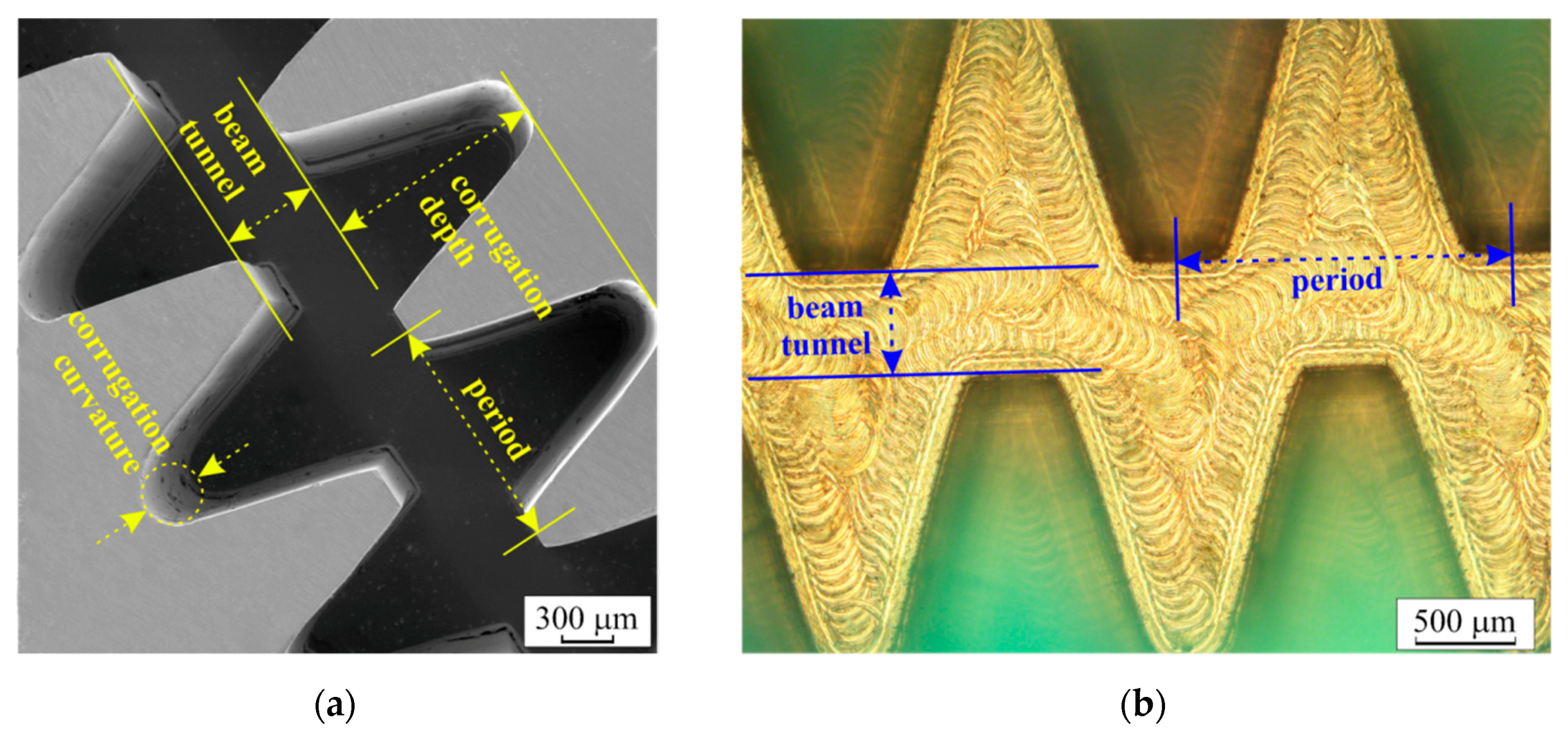
2. Design, Fabrication, and Morphology Studies

Performance of a BWO is influenced by the SWS [5]. The sinusoidally-corrugated waveguide SWS is one of the most promising for operation in millimeter and terahertz band because it has good transmission performance, reduced ohmic loss, and excellent heat-dissipation properties due to its all-metal structure. To further improve the interaction impedance, a TSW SWS was proposed [16]. The TSW SWS is convenient for use with a sheet electron beam because there is no need for machining a small-size beam tunnel [17]. Figure 2 illustrates the design of the TSW SWS circuit proposed in [15]. A 10-pitch regular TSW section, two 12-pitch tapered sections with a gradual reduction in corrugation depth, WR-15 rectangular waveguide sections, and input/output ports in the form of the UG-385/U flange comprise the design. The tapered 12-pitch sections are utilized to reduce reflections and offer a wideband-matched transition to a WR-15 rectangular waveguide. The dimensions of the interaction structure are the following [15]: Waveguide width a = 3.6 mm, waveguide height b = 1.8 mm, corrugation depth hc = 1.435 mm, period d = 1.4 mm, and beam tunnel height ht = 0.55 mm. The sine waveguide is a waveguide having sinusoidally corrugated E-planes, the profiles of which in the H-plane are determined by the formula below (see Figure 2b) [15,16,17,18,19]:
f z = ± b 2 + h c b h t 2 sin 2 π z d .
Thus, the only difference from a regular sine waveguide is the truncation of the SWS surface near the beam tunnel, which causes field amplification and increases the interaction impedance [16,17,18].
The basic design principle of the SWS is the following. The waveguide width a primarily determines the operating frequency since the lower cut-off is the same as of the TE01-mode in a rectangular waveguide, ω c = π c / a . The SWS period is determined by the operating voltage. For example, if the beam-wave synchronism should be attained with the fundamental backward harmonic in the center of passband, then β 0 = π / 2 d and d = π v 0 / 2 ω 0 , see Figure 1b. The corrugation depth hc influences the bandwidth of the SWS. Increase of the corrugation depth causes an increase in the slow-down factor and a decrease in the bandwidth. Actually, hc is mainly determined by the dimension of mills used for microfabrication.
The proposed interaction structure was fabricated by using CNC micromilling. The DMC 635 V Ecoline (DMG MORI, Nakamura-ku, Nagoya, Japan/Bielefeld, Germany), a 3-axis CNC vertical machining center, was chosen because of its positioning accuracy in the XYZ axes, which is no worse than 6 microns. In order to microfabricate the central part of the SWS, the mills with diameter from 500 down to 300 microns were selected (JJTOOLS Co., Ltd., Seoul, Korea).
The first sample of the SWS was made from the aluminum–magnesium alloy (A 95546/A 95556) to verify and tune the micromilling process [20]. The final sample of the interaction structure was made from the oxygen-free copper. Photos of the fabricated samples are shown in Figure 3. The upper plate served as a cover, while the circuit was solely engraved on the lower plate. While the corrugation section of the final structure was formed using mills with a diameter of 300 micron, the beam channel was made using mills with a diameter of 500 micron. Mills with a diameter of 500 microns were also used to fabricate the straight waveguide segments.
In order to verify the dimensions and surface roughness of the fabricated samples, we used optical inspection microscopy (MX51, Olympus, Tokyo, Japan), scanning electron microscopy (Mira II microscope, Tescan, Brno, Czech Republic), and surface profilometry (Dektak 150, Veeco Inc., Plainview, NY, USA).
The findings of the morphological studies of the interaction structure fabricated of oxygen-free copper are presented in Figure 4. The results of the analysis of the morphological studies by scanning electron and optical microscopy are summarized in Table 1. The dimensions of the fabricated interaction structure are in good agreement with the numerical model except for the corrugation depth and corrugation curvature. This is mainly due to the used mills with a certain diameter of 300 μm. This problem is typical for fabrication of sine-waveguide SWS by micromachining [21].
Figure 5 illustrates the outcomes of the surface roughness investigations. It shows that the surface roughness (root mean square) value is less than 102 nm.
The results of the morphological study demonstrate that the corrugation profile in the microfabricated interaction structure slightly differs from the design. As a result, the previously indicated shape f(z) (1) does not exactly match the corrugation profile. It actually has a form that is comprised of two almost straight lines and a semicircle with an empirically determined corrugation diameter that is nearly equal to the diameter of the mills used. Therefore, the numerical model was modified to match the experimentally measured dimensions. The transformation of the corrugation profile is illustrated in Figure 6. The corrugation depth hc in the microfabricated interaction structure is clearly reduced (see Figure 6, where δ indicates the difference between the corrugation depth in the original numerical model and in the microfabricated sample). As a result, we apply the numerical model with a modified corrugation profile to verify the electromagnetic parameters acquired from the experimental measurements.

3. Cold-Test Studies

The cold-test measurements of the copper-made interaction structure were carried out with the help of an experimental setup (see Figure 7a) based on the vector network analyzer (PNA N5227A, Keysight Technologies, Santa Rosa, USA). In order to connect the interaction structure to the VNA, waveguide to coax adapters (PTC-15VF-01, Ducommun, Santa Ana, USA) and coax cables were used (SC-185-MF-24, Maury Microwave, Ontario, USA). Prior to the experiments, a complete two-port TRL type calibration procedure was performed, utilizing a mechanical calibration kit on waveguide end adapters (V11644A, Keysight Technologies, Santa Rosa, USA). Figure 7b shows the results of the S-parameter cold-test measurement along with a comparison with the results of numerical simulation by using CST Studio Suite. In the numerical model, the material of the circuit is set to copper with an effective conductivity of 2.0 × 10⁷ S/m, taking into consideration the influence of surface roughness. The reflection loss was found to be no worse than 10 dB, whereas the transmission loss ranged from 4 to 6 dB. Fabrication tolerance, local copper surface oxidations, and less-than-ideal connections between measuring flanges and the fabricated structure are all factors that contribute to the minor differences between measurement and simulation. There were no significant associations between small deviations in measurement and simulation data.
In the next step, we retrieved dispersion of the fabricated structure using measured phase data of the transmitted signal. The method of reconstruction is illustrated in Figure 8 (see also [22,23]). First, we plot the dependency of the phase of the transmitted signal versus frequency. Then, we select all the frequency points where we observe the phase jumps from −π to π. The first point of the phase jump has a phase shift on the dispersion plot that is equal to 2π. The phase shift of the second point of the phase jump is 2π − Δ, where Δ = 2 π / M , M is the number of the pitches of the interaction structure. The number of pitches in the fabricated structure is 34, which is the sum of the 10 regular pitches and 2 × 12 tapered pitches (see Figure 2a). Consequently, the phase shift of the third point of the phase jump will be 2π – 2 × Δ and accordingly 2π − (n − 1) × Δ for the n-th point. A comparison of the dispersion characteristic retrieved from the experimental data and from the numerical simulation is presented in Figure 9. Table 2 also includes a comprehensive comparison of the dispersion parameters derived from numerical simulations and determined from experimental findings. The differences between experimentally acquired and numerically derived data are calculated as well. The difference was revealed to be less than 0.9%. The last demonstrates the good agreement between experimental observations and numerical modeling.
In addition, the dispersion characteristic for the initial design [15] is plotted in Figure 9; it shows a significant difference with the experimental. In particular, the high-frequency cut-off is ~5 GHz less, which is attributed to deeper corrugation (see Figure 6).

4. Conclusions

The TSW interaction structure for a high-power V-band sheet-beam BWO proposed in [15] was successfully fabricated by CNC micromachining. Morphological studies of the lateral dimensions demonstrated good agreement with the numerical model except for the corrugation depth. The primary reason behind this is the following: the applied mills, namely their diameter, limit the actual acquired resolution of the microfabricated structure, regardless of the fact that the command resolution of the utilized CNC micromilling machine itself is up to 1 μm. The diameter of the employed mills was aptly illustrated (see Figure 5) to be higher than the corrugation curvature in the numerical model. As a result of the constraints of the cutting tools currently in use, the corrugation profile of the interaction structure cannot be microfabricated as the perfect sine. This problem is typical for fabrication of sine-waveguide SWS by micromachining [21]. Therefore, we adjusted the numerical model of the interaction structure in order to match the experimentally measured dimensions. According to measurements of surface roughness, the root mean square value of the roughness is less than 102 nm, which is less than the copper skin depth at V-band frequencies. The cold-test measurement of electromagnetic parameters of the SWS indicates a strong agreement with the numerical simulations. The reflection loss was found to be no worse than 10 dB, whereas the transmission loss varied from 4 to 6 dB. Minor discrepancies between measurement and simulation are caused by fabrication tolerance, local copper surface oxidations, and less-than-ideal connections between measuring flanges and the fabricated structure. Furthermore, the measured data were used to reconstruct the dispersion of the fabricated interaction structure. The experimental results are in good agreement with the numerical simulation.

Author Contributions

Conceptualization, N.R. and N.K.; methodology, A.S., A.P. and A.A.; software, R.T. and V.T.; validation, A.S. and V.G.; investigation, V.G. and A.P.; data curation, V.T.; writing—original draft preparation, A.S.; writing—review and editing, N.R. and N.K.; visualization, V.T.; project administration, N.R. All authors have read and agreed to the published version of the manuscript.

Funding

This research was funded by Russian Science Foundation under grant # 22-49-02017 and by the Department of Science and Technology (DST), India under grant # DST/IC/RSF/2022/280.

Data Availability Statement

The data that support the findings of this study are available from the corresponding author upon reasonable request.

Conflicts of Interest

The authors declare no conflict of interest.

References

  1. Booske, J.H.; Dobbs, R.J.; Joye, C.D.; Kory, C.L.; Neil, G.R.; Park, G.-S.; Park, J.; Temkin, R.J. Vacuum electronic high power terahertz sources. IEEE Trans. Terahertz Sci. Technol. 2011, 1, 54–75. [Google Scholar] [CrossRef]
  2. Lewis, R.A. A review of terahertz sources. J. Phys. D Appl. Phys. 2014, 47, 374001. [Google Scholar] [CrossRef]
  3. Niu, Y.; Li, Y.; Jin, D.; Su, L.; Vasilakos, A.V. A survey of millimeter wave communications (mmWave) for 5G: Opportunities and challenges. Wirel. Networks 2015, 21, 2657–2676. [Google Scholar] [CrossRef]
  4. Borisov, A.A.; Budzinsky, U.A.; Bykovsky, S.V.; Galdetskiy, A.V.; Korolev, A.N.; Lopin, M.I.; Negirev, A.A.; Pugnin, V.I.; Ruvinsky, G.V.; Sazonov, B.V. The development of vacuum microwave devices in Istok. In Proceedings of the 2011 IEEE International Vacuum Electronics Conference (IVEC), Bangalore, India, 21–24 February 2011; IEEE: Piscataway, NJ, USA, 2011; pp. 437–438. [Google Scholar]
  5. Grigoriev, A.D.; Ivanov, V.A.; Molokovsky, S.I. Microwave Electronics; Springer Series in Advanced Microelectronics; Springer International Publishing: Cham, Switzerland, 2018; Volume 61, ISBN 978-3-319-68890-9. [Google Scholar]
  6. Christiansen, J.; Schultheiss, C. Production of high current particle beams by low pressure spark discharges. Z. Phys. A Atoms Nucl. 1979, 290, 35–41. [Google Scholar] [CrossRef]
  7. Yin, H.; Zhang, L.; Xie, J.; Ronald, K.; He, W.; Shu, G.; Zhao, J.; Yin, Y.; Chen, X.; Alfadhl, Y.; et al. Compact high-power millimetre wave sources driven by pseudospark-sourced electron beams. IET Microw. Antennas Propag. 2019, 13, 1794–1798. [Google Scholar] [CrossRef]
  8. Wong, C.S.; Woo, H.J.; Yap, S.L. A low energy tunable pulsed X-ray source based on the pseudospark electron beam. Laser Part. Beams 2007, 25, 497–502. [Google Scholar] [CrossRef]
  9. Lebedev, S.V.; Machida, M.; Moshkalyov, S.A.; Campos, D.O. Experimental study of the pseudospark-produced electron beam for material processing. IEEE Trans. Plasma Sci. 1997, 25, 754–757. [Google Scholar] [CrossRef]
  10. He, W.; Zhang, L.; Bowes, D.; Yin, H.; Ronald, K.; Phelps, A.D.R.; Cross, A.W. Generation of broadband terahertz radiation using a backward wave oscillator and pseudospark-sourced electron beam. Appl. Phys. Lett. 2015, 107, 133501. [Google Scholar] [CrossRef]
  11. Zhang, L.; Yin, H.; He, W.; Chen, X.; Zhang, J.; Cross, A. Pseudospark-sourced beam and its application in high-power millimeter-wave generation. Sci. Rep. 2021, 11, 19076. [Google Scholar] [CrossRef] [PubMed]
  12. Singhal, K.; Gurjar, N.; Jain, S.; Vishant; Abhishek, A.; Starodubov, A.V.; Ryskin, N.M.; Kumar, N. Analysis of hollow cathode aperture wall profile on pseudospark discharge-based sheet electron beam source. IEEE Trans. Plasma Sci. 2021, 49, 302–306. [Google Scholar] [CrossRef]
  13. Kumar, N.; Abhishek, A.; Vishant; Singhal, K.; Gurjar, N.; Jain, S.; Starodubov, A.V.; Ryskin, N.M. Pseudospark-driven high-current miniaturized voltage-tunable sheet-electron-beam source. IEEE Trans. Electron Devices 2021, 68, 6482–6486. [Google Scholar] [CrossRef]
  14. Ryskin, N.M.; Rozhnev, A.G.; Starodubov, A.V.; Serdobintsev, A.A.; Pavlov, A.M.; Benedik, A.I.; Torgashov, R.A.; Torgashov, G.V.; Sinitsyn, N.I. Planar microstrip slow-wave structure for low-voltage V-band traveling-wave tube with a sheet electron beam. IEEE Electron Device Lett. 2018, 39, 757–760. [Google Scholar] [CrossRef]
  15. Torgashov, R.A.; Titov, V.N.; Vishant; Kumar, N.; Abhishek, A.; Gurjar, N.; Singhal, K.; Jain, S.; Sharma, R.K.; Ryskin, N.M. Investigations on high-current-density sheet-beam driven v-band slow wave oscillator with a hollow cathode. IEEE Trans. Plasma Sci. 2021, 49, 263–268. [Google Scholar] [CrossRef]
  16. Fang, S.; Xu, J.; Yin, H.; Lei, X.; Jiang, X.; Yin, P.; Wu, G.; Yang, R.; Li, Q.; Guo, G.; et al. experimental verification of the low transmission loss of a flat-roofed sine waveguide slow-wave structure. IEEE Electron Device Lett. 2019, 40, 808–811. [Google Scholar] [CrossRef]
  17. Fang, S.; Xu, J.; Jiang, X.; Lei, X.; Wu, G.; Li, Q.; Ding, C.; Yu, X.; Wang, W.; Gong, Y.; et al. Study on W-band sheet-beam traveling-wave tube based on flat-roofed sine waveguide. AIP Adv. 2018, 8, 055116. [Google Scholar] [CrossRef]
  18. Xu, X.; Wei, Y.; Shen, F.; Duan, Z.; Gong, Y.; Yin, H.; Wang, W. Sine waveguide for 0.22-THz traveling-wave tube. IEEE Electron Device Lett. 2011, 32, 1152–1154. [Google Scholar] [CrossRef]
  19. Xu, X.; Wei, Y.; Shen, F.; Yin, H.; Xu, J.; Gong, Y.; Wang, W. A watt-class 1-THz backward-wave oscillator based on sine waveguide. Phys. Plasmas 2012, 19, 013113. [Google Scholar] [CrossRef]
  20. Starodubov, A.; Torgashov, R.; Rozhnev, A.; Pavlov, A.; Zakharevich, A.; Ryskin, N.; Jain, S.; Vishant; Kumar, N. Fabrication and characterization of a slow-wave structure for the v-band backward-wave oscillator with a pseudospark-source electron gun. In Proceedings of the 2021 46th International Conference on Infrared, Millimeter and Terahertz Waves (IRMMW-THz), Chengdu, China, 29 August–3 September 2021; IEEE: Piscataway, NJ, USA, 2021; pp. 1–2. [Google Scholar] [CrossRef]
  21. Choi, W.; Lee, I.; Choi, E. Design and Fabrication of a 300 GHz Modified Sine Waveguide Traveling-Wave Tube Using a Nanocomputer Numerical Control Machine. IEEE Trans. Electron Devices 2017, 64, 2955–2962. [Google Scholar] [CrossRef]
  22. Shu, G.; Liao, J.; Ren, J.; He, J.; Deng, J.; Chang, Z.; Xu, B.; Wang, G.; Ruan, C.; He, W. Dispersion and dielectric attenuation properties of a wideband double-staggered grating waveguide for subterahertz sheet-beam traveling-wave amplifiers. IEEE Trans. Electron Devices 2021, 68, 5826–5833. [Google Scholar] [CrossRef]
  23. Baik, C.-W.; Ahn, H.Y.; Kim, Y.; Lee, J.; Hong, S.; Choi, J.H.; Kim, S.; Lee, S.H.; Jun, S.Y.; Yu, S.; et al. Dispersion retrieval from multi-level ultra-deep reactive-ion-etched microstructures for terahertz slow-wave circuits. Appl. Phys. Lett. 2014, 104, 021118. [Google Scholar] [CrossRef]
Figure 1. Schematic of the proposed BWO (a) and dispersion diagram (b) illustrating beam-wave synchronism.
Electronics 11 02858 g001
Figure 2. Schematic drawing of the proposed interaction structure: (a) view of the full-scale circuit; (b) an enlarged view of a single period in the regular 10-pitch section.
Electronics 11 02858 g002
Figure 3. Photos of the fabricated by CNC micromilling samples of the proposed interaction structure: (a) an aluminum-made interaction structure; (b) the final sample of the interaction structure made from oxygen-free copper.
Electronics 11 02858 g003
Figure 4. Results of the morphology studies: (a) SEM image of the central part of the final sample of the interaction structure; (b) image from the optical inspection microscope of the central part of the fabricated interaction structure.
Electronics 11 02858 g004
Figure 5. Results of the surface roughness studies of the final sample.
Electronics 11 02858 g005
Figure 6. An illustration showing how the initial corrugation profile (in blue) changed throughout the micromilling fabrication process. The red color indicates the corrugation profile that has been adjusted following the micromilling operation. A dashed green line represents a simplified version of the corrugation profile, which includes the hemicircle and straight lines. Δ indicates the difference between the corrugation depth in the original numerical model and the corrugation depth in the microfabricated sample of the interaction structure.
Electronics 11 02858 g006
Figure 7. (a) A photo of the experimental equipment used for cold-test measurements. The numbers denote: 1—Copper-made full-length interaction structure, 2—Coax-to-waveguide adapters, 3—Coaxial cables, 4—vector network analyzer; (b) a comparison of the experimental data (blue) and numerical simulation (red): the solid lines represent the reflection losses, while the dashed lines denote the transmission losses.
Electronics 11 02858 g007
Figure 8. Illustration of the reconstruction of the dispersion characteristic from the experimentally measured phase data.
Electronics 11 02858 g008
Figure 9. Comparison of the experimentally measured dispersion characteristic with the numerically simulated for the initial model and the model with modified corrugation profile.
Electronics 11 02858 g009
Table 1. Dimensional comparison between the original numerical model and the microfabricated sample.
NameNumerical ModelMicrofabricated Structure
Beam tunnel height, ht (μm)550553.49 ± 6.06
Corrugation depth, hc (μm)14351259.6 ± 12.14
Corrugation curvature (μm)is determined by the f(z)319.13 ± 8.65
Period, d (μm)14001402.38 ± 3.63
Table 2. A comparison of the dispersion characteristics obtained from the numerical simulations and reconstructed from the experimental measurements.
Point
Number
Phase Shift (Rad)Frequency (GHz)
Simulation Data
Frequency (GHz)
Experimental Data
Difference, %
1 6.28341.72441.4250.72
2 6.09842.02841.8190.50
3 5.91442.53742.4190.28
4 5.72943.22243.2060.04
5 5.54444.08744.163−0.17
6 5.35945.13245.288−0.34
7 5.17446.31046.563−0.55
8 4.99047.65047.988−0.71
9 4.80549.10049.488−0.79
10 4.62050.67451.119−0.88
11 4.43552.32352.786−0.89
12 4.25054.05754.541−0.89
13 4.06655.86956.356−0.87
14 3.88157.70158.215−0.89
15 3.69659.59460.081−0.82
16 3.51161.50961.919−0.67
17 3.32663.40463.719−0.50
18 3.14265.31665.463−0.22
19 2.95767.16867.0940.11
20 2.77268.96068.6130.50
21 2.58770.677
22 2.40272.241
23 2.21873.630
24 2.03374.831
25 1.84875.756
26 1.66376.435
27 1.47876.842
28 1.29477.043
Publisher’s Note: MDPI stays neutral with regard to jurisdictional claims in published maps and institutional affiliations.

