
A Self-Tuned Method for Impedance-Matching of Planar-Loop Resonators in Conformable Wearables


Abstract
:1. Introduction
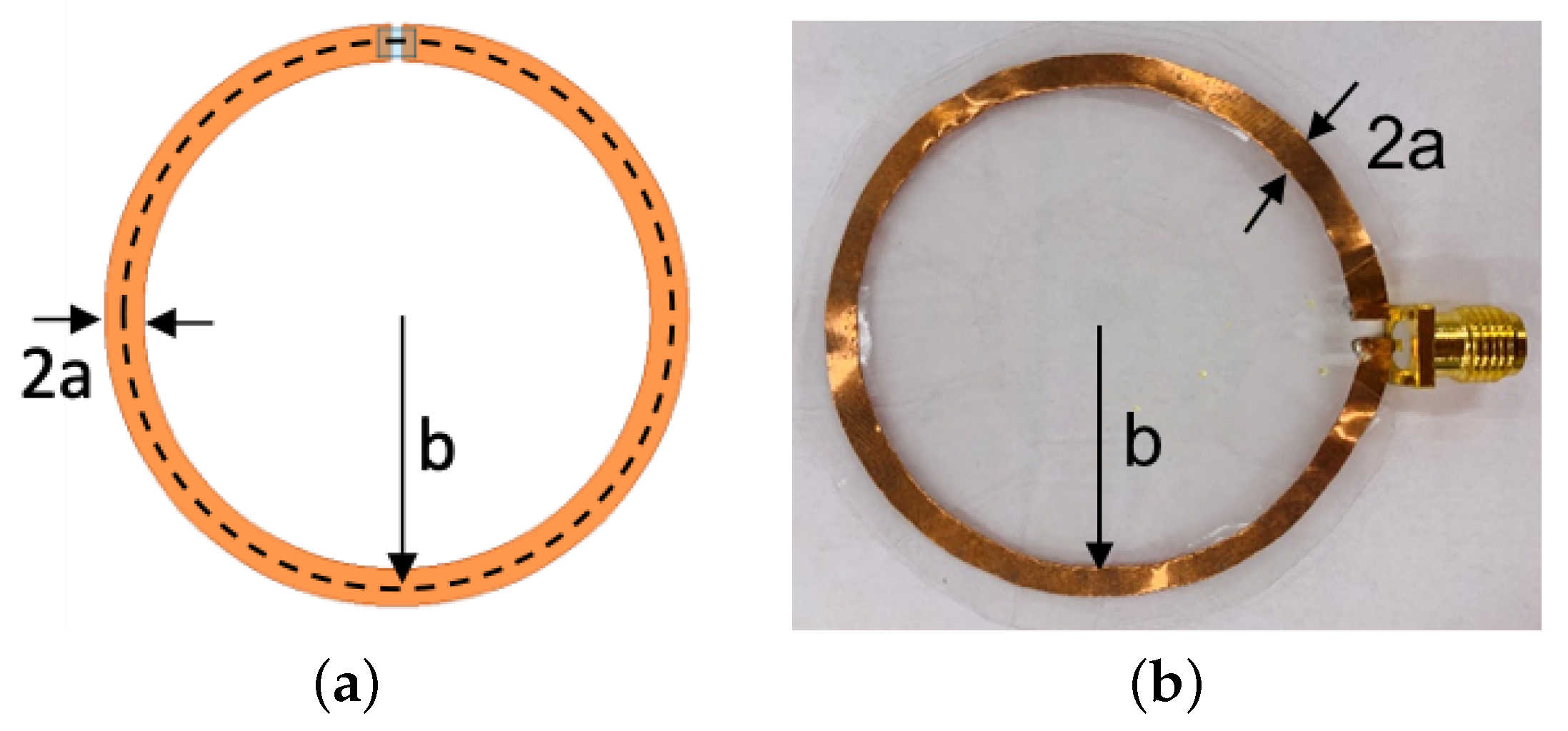
2. Limitations of Loop Resonators
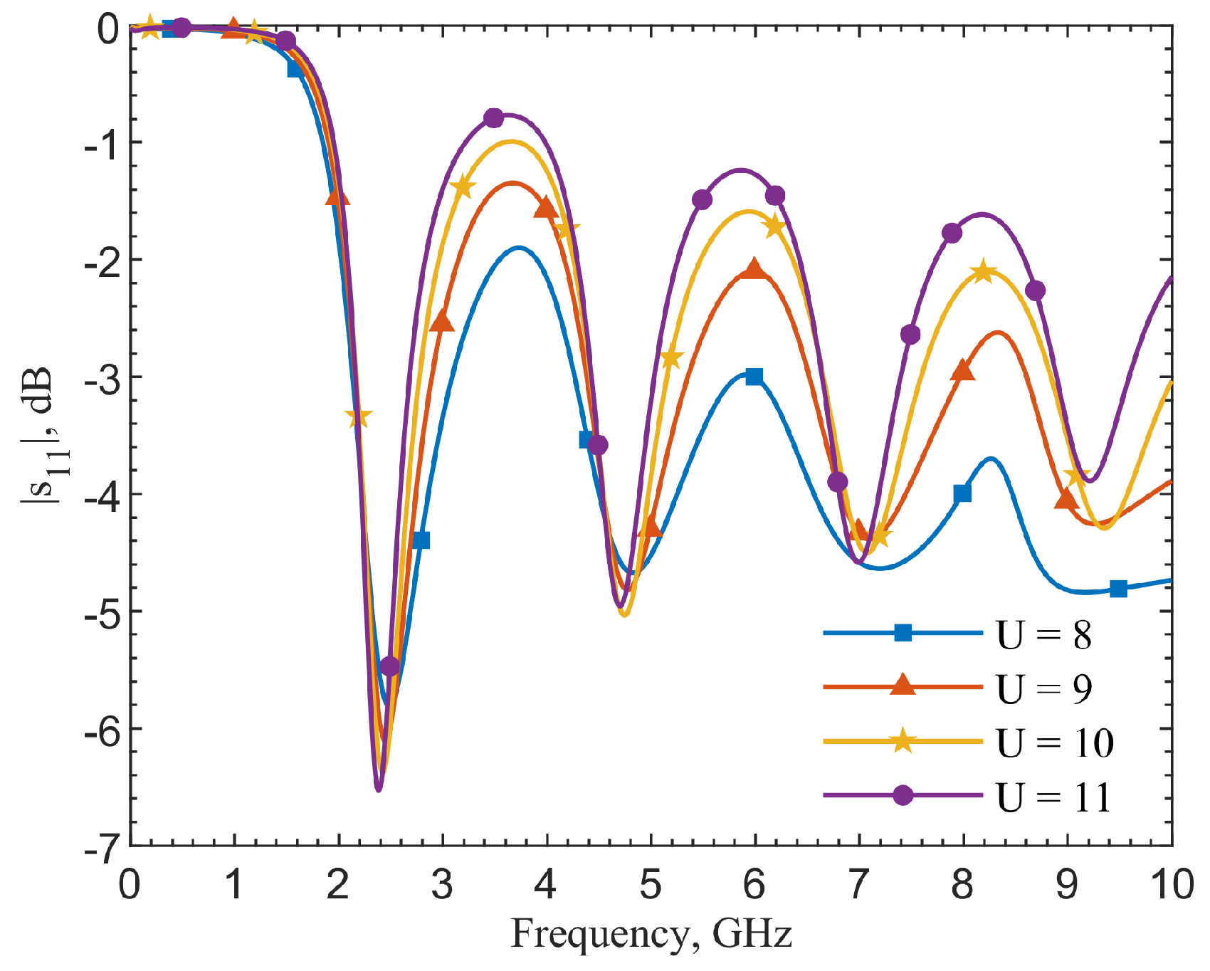
2.1. Simulations
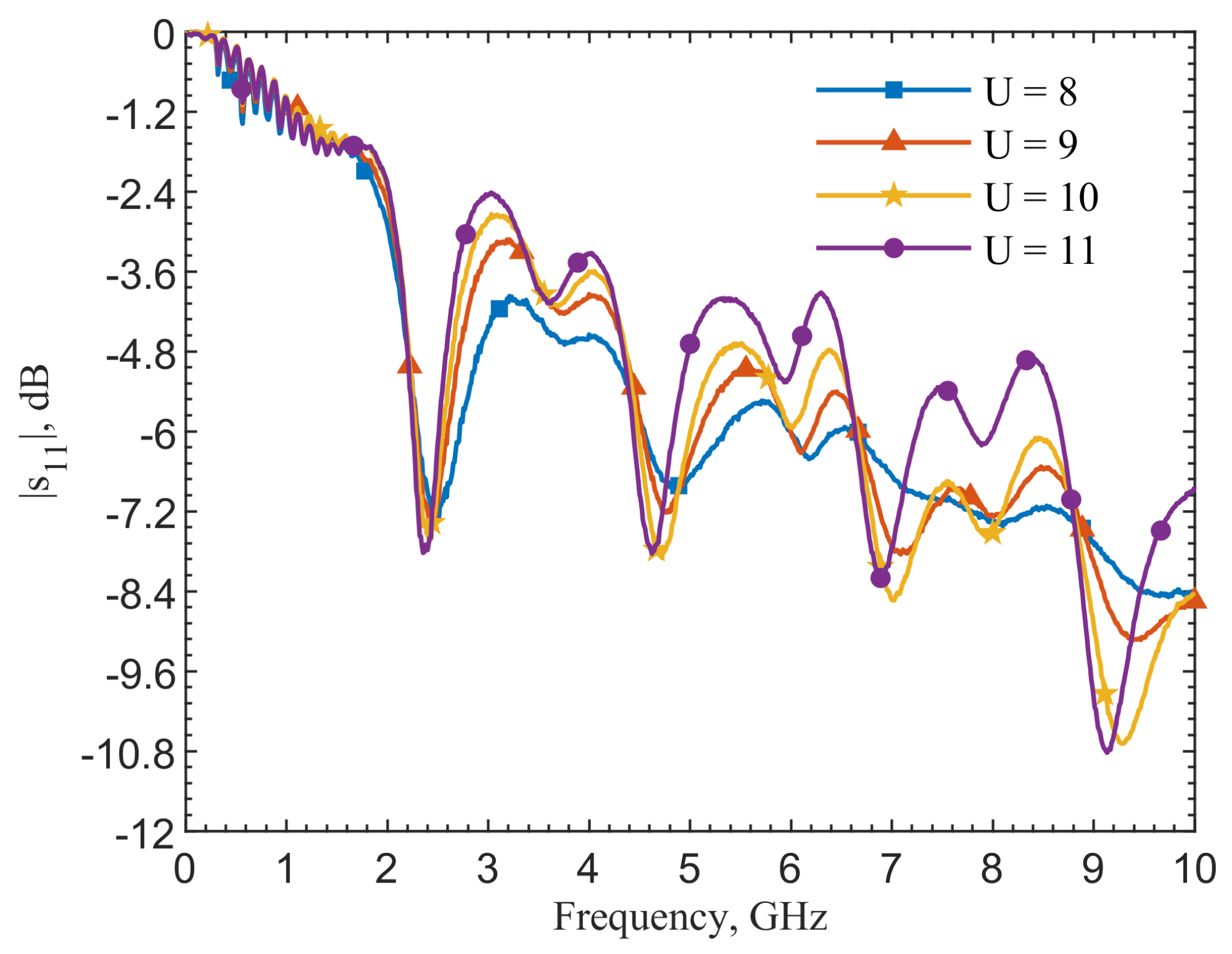
2.2. Measurements
2.3. Comparison of Each U
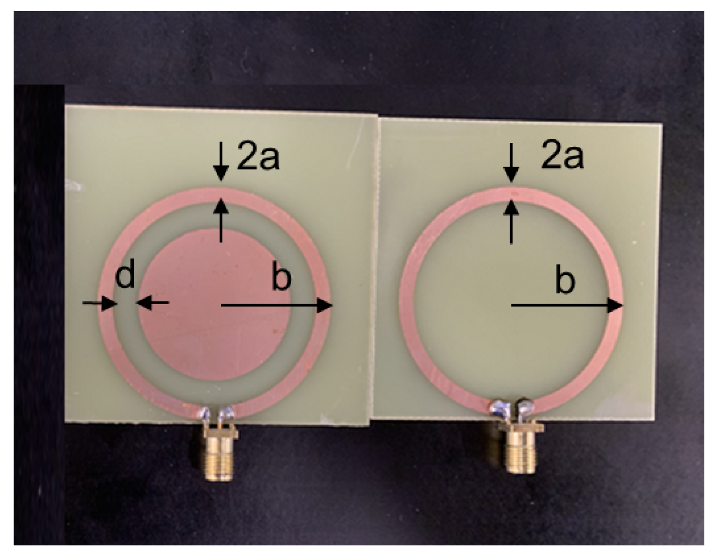
3. Tuned Resonator Design
3.1. Tuning Mechanism
3.2. Finite-Element Simulations
3.3. Equivalent Circuits
4. Experimental Results
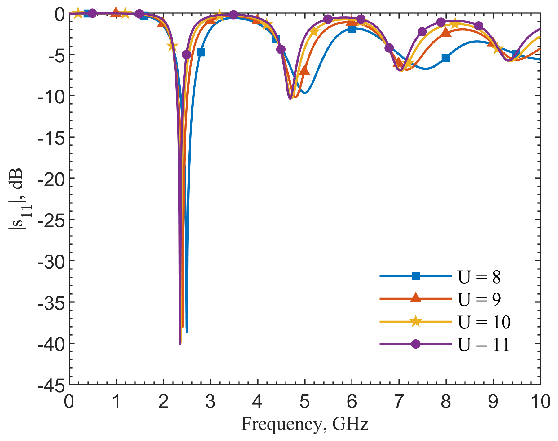
4.1. Results of The Self-Tuned Loop Resonator with U = 9
4.2. Optimal d for U
5. Discussion
5.1. Discrepancy Investigation
5.2. Effect of Substrate
6. Conclusions
Author Contributions
Funding
Institutional Review Board Statement
Informed Consent Statement
Data Availability Statement
Acknowledgments
Conflicts of Interest
References
- Pendry, J.; Holden, A.; Robbins, D.; Stewart, W. Magnetism from Conductors and Enhanced Nonlinear Phenomena. IEEE Trans. Microw. Theory Tech. 1999, 47, 2075–2084. [Google Scholar] [CrossRef]
- Marqués, R.; Martín, F.; Sorolla, M. Metamaterials with Negative Parameters: Theory, Design, and Microwave Applications, 1st ed.; Wiley: Hoboken, NJ, USA, 2008; Volume 183. [Google Scholar]
- Chowdhury, D.R.; Singh, R.; Reiten, M.; Chen, H.T.; Taylor, A.J.; O’Hara, J.F.; Azad, A.K. A Broadband Planar Terahertz Metamaterial with Nested Structure. Opt. Express 2011, 19, 15817–15823. [Google Scholar] [CrossRef]
- Rockstuhl, C.; Zentgraf, T.; Guo, H.; Liu, N.; Etrich, C.; Loa, I.; Syassen, K.; Kuhl, J.; Lederer, F.; Giessen, H. Resonances of Split-ring Resonator Metamaterials in the Near Infrared. Appl. Phys. B Lasers Opt. 2006, 84, 219–227. [Google Scholar] [CrossRef]
- Delgado, V.; Sydoruk, O.; Tatartschuk, E.; Marqués, R.; Freire, M.; Jelinek, L. Analytical Circuit model for Split Ring Resonators in the Far Infrared and Optical Frequency Range. Metamaterials 2009, 3, 57–62. [Google Scholar] [CrossRef]
- Enkrich, C.; Wegener, M.; Linden, S.; Burger, S.; Zschiedrich, L.; Schmidt, F.; Zhou, J.F.; Koschny, T.; Soukoulis, C.M. Magnetic Metamaterials at Telecommunication and Visible Frequencies. Phys. Rev. Lett. 2005, 95, 203901. [Google Scholar] [CrossRef] [PubMed]
- Locatelli, A. Peculiar Properties of Loop Nanoantennas. IEEE Photonics J. 2005, 3, 845–853. [Google Scholar] [CrossRef]
- Aydin, K.; Bulu, I.; Guven, K.; Kafesaki, M.; Soukoulis, C.M.; Ozbay, E. Investigation of Magnetic Resonances for Different Split-ring Resonator Parameters and Designs. New J. Phys. 2005, 7, 168. [Google Scholar] [CrossRef]
- Baghelani, M.; Abbasi, Z.; Daneshmand, M.; Light, P.E. Non-invasive Continuous-time Glucose Monitoring System Using a Chipless Printable Sensor Based on Split Ring Microwave Resonators. Sci. Rep. 2020, 10, 12980. [Google Scholar] [CrossRef] [PubMed]
- Ekinci, G.; Calikoglu, A.; Solak, S.N.; Yalcinkaya, A.D.; Dundar, G.; Torun, H. Split-ring Resonator-based Sensors on Flexible Substrates for Glaucoma Monitoring. Sens. Actuators A Phys. 2020, 268, 32–37. [Google Scholar] [CrossRef]
- Choi, H.; Naylon, J.; Luzio, S.; Beutler, J.; Birchall, J.; Martin, C.; Porch, A. Design and In Vitro Interference Test of Microwave Noninvasive Blood Glucose Monitoring Sensor. IEEE Trans. Microw. Theory Tech. 2015, 63, 3016–3025. [Google Scholar] [CrossRef] [PubMed] [Green Version]
- Choi, H.; Luzio, S.; Beutler, J.; Porch, A. Microwave Noninvasive Blood Glucose Monitoring Sensor: Human Clinical Trial Results. In Proceedings of the 2017 IEEE MTT-S International Microwave Symposium (IMS), Honolulu, HI, USA, 4–9 June 2017; IEEE: Piscataway, NJ, USA, 2017; pp. 876–879. [Google Scholar]
- Torun, H.; Top, F.C.; Dundar, G.; Yalcinkaya, A.D. A Split-ring Resonator-based Microwave Sensor for Biosensing. In Proceedings of the 2014 International Conference on Optical MEMS and Nanophotonics, Glasgow, UK, 17–21 August 2014; University of Strathclyde: Glasgow, UK, 2014; pp. 159–160. [Google Scholar]
- Mueh, M.; Damm, C. Spurious Material Detection on Functionalized Thin-Film Sensors using Multiresonant Split-Rings. In Proceedings of the 2018 IEEE International Microwave Biomedical Conference (IMBioC), Philadelphia, PA, USA, 14–15 June 2018; IEEE: Piscataway, NJ, USA, 2018; pp. 196–198. [Google Scholar]
- Storer, J.E. Impedance of Thin-wire Loop Antennas. Trans. Am. Inst. Electr. Eng. Part 1 Commun. Electron. 1956, 75, 606–619. [Google Scholar] [CrossRef]
- Wu, T.T. Theory of the Thin Circular Loop Antenna. J. Math. Phys. 1962, 3, 1301–1304. [Google Scholar] [CrossRef]
- McKinley, A.F.; White, T.P.; Maksymov, I.S.; Catchpole, K.R. The Analytical Basis for the Resonances and Anti-resonances of Loop Antennas and Meta-material Ring Resonators. J. Appl. Phys. 2012, 112, 94911. [Google Scholar] [CrossRef]
- Wei, J. Distributed Capacitance of Planar Electrodes in Optic and Acoustic Surface Wave Devices. IEEE J. Quantum Electron. 1977, 13, 152–158. [Google Scholar] [CrossRef]
- Maradei, F.; Caniggia, S. Appendix A: Formulae for Partial Inductance Calculation. In Signal Integrity and Radiated Emission of High-Speed Digital Systems; Francescaromana, M., Caniggia, S., Eds.; John Wiley & Sons, Ltd.: Chichester, UK, 2008; pp. 481–486. [Google Scholar]
- Bing, S.; Chawang, K.; Chiao, J.C. Resonant Coupler Designs for Subcutaneous Implants. In Proceedings of the 2021 IEEE Wireless Power Transfer Conference (WPTC), San Diego, CA, USA, 1–4 June 2021; IEEE: Piscataway, NJ, USA, 2021; pp. 1–4. [Google Scholar]
- Bing, S.; Chawang, K.; Chiao, J.C. A Resonant Coupler for Subcutaneous Implant. Sensors 2021, 21, 8141. [Google Scholar] [CrossRef] [PubMed]
- Bing, S.; Chawang, K.; Chiao, J.C. A Radio-Frequency Planar Resonant Loop for Noninvasive Monitoring of Water Content. In Proceedings of the 2022 IEEE Sensors, Dallas, TX, USA, 30 October–2 November 2022; IEEE: Piscataway, NJ, USA, 2022; pp. 1–4. [Google Scholar]


| U | R, ohm | L, nH | C, pF | |||||||||||
|---|---|---|---|---|---|---|---|---|---|---|---|---|---|---|
| 8 | 0.002 | 156.283 | 221.618 | 273.744 | 293.871 | 72.6 | 26.579 | 23.156 | 20.676 | 19.48 | 0.135 | 0.04 | 0.02 | 0.013 |
| 9 | 151.178 | 208.164 | 250.683 | 281.101 | 33.778 | 30.509 | 28.152 | 26.455 | 0.114 | 0.033 | 0.016 | 0.01 | ||
| 10 | 147.551 | 201.102 | 239.225 | 270.723 | 40.593 | 37.29 | 34.935 | 33.11 | 0.1 | 0.028 | 0.014 | 0.008 | ||
| 11 | 145.041 | 196.212 | 232.703 | 261.49 | 47.487 | 44.151 | 41.751 | 39.914 | 0.088 | 0.025 | 0.012 | 0.007 | ||
| Modal resistance | Unitless reference value | k | Unitless variable | ||
| Self inductance | Unitless reference value | Effective permittivity | |||
| Self capacitance | Unitless reference value | The impedance of free space | |||
| Modal impedance | Unitless reference value | The permeability of free space | |||
| Total distributed capacitance | Lommel–Weber function of order m | The permittivity of free space | |||
| Total capacitance | Bessel function of the first kind | a | The radius of a metal wire | ||
| Mutual inductance | Fundamental resonant frequency | b | The radius of the metal loop | ||
| Unitless reference value | m | The number of harmonic order |
| d, | , | , | , | , | , | , |
|---|---|---|---|---|---|---|
| 0.5 | 0.133 | 16.742 | 0.248 | 17.037 | 0.216 | 20.772 |
| 1 | 0.107 | 14.683 | 0.221 | 19.095 | 0.191 | 23.178 |
| 1.5 | 0.092 | 13.303 | 0.206 | 20.475 | 0.179 | 24.31 |
| 1.9 | 0.083 | 12.422 | 0.198 | 21.356 | 0.171 | 25.53 |
| 3 | 0.067 | 10.579 | 0.182 | 23.199 | 0.164 | 26.15 |
| 5 | 0.051 | 8.203 | 0.165 | 25.576 | 0.159 | 26.28 |
| d, mm | R, ohm | L, nH | C, pF | |||||||||||
|---|---|---|---|---|---|---|---|---|---|---|---|---|---|---|
| 0.5 | 0.002 | 25.125 | 49.81 | 71.13 | 91.345 | 72.6 | 20.772 | 18.791 | 15.768 | 12.602 | 0.216 | 0.059 | 0.031 | 0.022 |
| 1 | 35.88 | 67.25 | 97.86 | 120.13 | 23.178 | 20.142 | 15.831 | 13.595 | 0.191 | 0.055 | 0.031 | 0.02 | ||
| 1.5 | 45.22 | 82.565 | 114.39 | 141.565 | 24.31 | 20.243 | 15.166 | 11.46 | 0.179 | 0.054 | 0.032 | 0.023 | ||
| 1.9 | 49.48 | 92.635 | 117.84 | 137.86 | 25.53 | 19.092 | 12.795 | 8.016 | 0.171 | 0.056 | 0.037 | 0.032 | ||
Publisher’s Note: MDPI stays neutral with regard to jurisdictional claims in published maps and institutional affiliations. |
© 2022 by the authors. Licensee MDPI, Basel, Switzerland. This article is an open access article distributed under the terms and conditions of the Creative Commons Attribution (CC BY) license (https://creativecommons.org/licenses/by/4.0/).
Share and Cite
Bing, S.; Chawang, K.; Chiao, J.-C. A Self-Tuned Method for Impedance-Matching of Planar-Loop Resonators in Conformable Wearables. Electronics 2022, 11, 2784. https://doi.org/10.3390/electronics11172784
Bing S, Chawang K, Chiao J-C. A Self-Tuned Method for Impedance-Matching of Planar-Loop Resonators in Conformable Wearables. Electronics. 2022; 11(17):2784. https://doi.org/10.3390/electronics11172784
Chicago/Turabian StyleBing, Sen, Khengdauliu Chawang, and J.-C. Chiao. 2022. "A Self-Tuned Method for Impedance-Matching of Planar-Loop Resonators in Conformable Wearables" Electronics 11, no. 17: 2784. https://doi.org/10.3390/electronics11172784