
An Interleaved Two Switch Soft-Switching Forward PWM Power Converter with Current Doubler Rectifier


Abstract
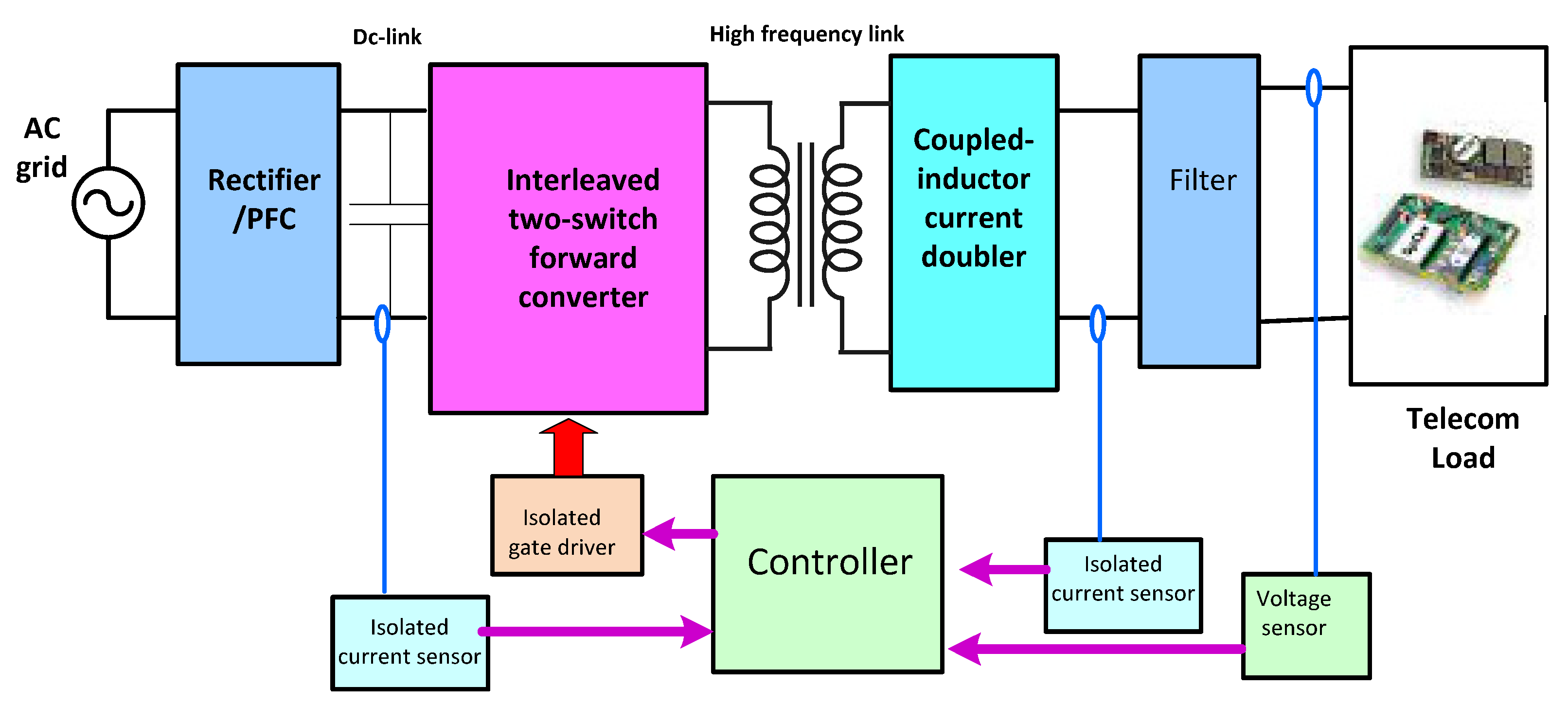
:1. Introduction
2. Principle of Operation
- All the active power switches and passive power components are ideal.
- High frequency transformers T1 and T2 are matching, so that every magnetizing and leakage inductances are characterized as Lp1 = Lp2 = Lp, Ls1 = Ls2 = Ls, respectively.
- Capacitors C1 and C2 are identical: C1 = C2 = C.
- Inductor Lo1 and Lo2 are coupled compactly and its coupling coefficient k ≈ 1.
3. Steady State Operational Characteristics
4. Experimental Results and Discussions
5. Discussion
6. Conclusions
- The switching losses are low through a wide-ranging of load variation.
- Circulating currents are low, resulting in a low amount of conduction losses.
- No need for using additional auxiliary snubber circuits.
- No existence of flux imbalance in the two high frequency transformer windings because of the existence of forward configuration of the converter.
Author Contributions
Funding
Data Availability Statement
Conflicts of Interest
References
- Sayed, K. ZVS Soft-Switched DC-DC Converter based Charger for Low Voltage battery in Hybrid Electric Vehicles. IET Power Electron. 2019, 12, 3389–3396. [Google Scholar] [CrossRef]
- Sayed, K.; Kwon, S.K.; Nishida, K.; Nakaoka, M. New DC Rail Side Soft-Switching PWM DC–DC Converter with Current Doubler Rectifier. In Proceedings of the IEEE Ninth International Conference Power Electronics and Drive Systems (PEDS), Singapore, 5–8 December 2011; pp. 687–694. [Google Scholar]
- Sayed, K.; Kwon, S.K.; Nishida, K.; Nakaoka, M. New DC Rail Side Soft-Switching PWM DC–DC Converter with Voltage Doubler Rectifier for PV Generation Interface. In Proceedings of the IEEE International Power Electronics Conference (IPEC—ECCE-ASIA), Hiroshima, Japan, 18–21 May 2014; pp. 2359–2365. [Google Scholar]
- Ashraf, N.; Izhar, T.; Abbas, G.; Awan, A.B.; Alghamdi, A.S.; Abo-Khalil, A.G.; Sayed, K.; Farooq, U.; Balas, V.E. A New Single-Phase Direct Frequency Controller Having Reduced Switching Count without Zero-Crossing Detector for Induction Heating System. Electronics 2020, 9, 430. [Google Scholar] [CrossRef]
- Saleeb, H.; Sayed, K.; Kassem, A.; Mostafa, R. Control and analysis of bidirectional interleaved hybrid converter with coupled inductors for electric vehicle applications. Electr. Eng. 2020, 102, 195–222. [Google Scholar] [CrossRef]
- Hamada, S.; Nakaoka, M. A Novel Zero-Voltage and Zero-Current Switching PWM DC-DC Converter with Reduced Conduction Losses. IEEE Trans. Power Electron. 2002, 17, 413–419. [Google Scholar] [CrossRef]
- Sayed, K.; Almutairi, N.; Albagami, N.; Alrumayh, O.; Abo-Khalil, A.G.; Saleeb, H. A Review of DC-AC Converters for Electric Vehicle Applications. Energies 2022, 15, 1241. [Google Scholar] [CrossRef]
- Kim, E.S.; Joe, K.Y.; Kye, M.H.; Kim, Y.H.; Yoon, B.D. An improved soft-switching PWM FB DC/DC converter for reducing conduction losses. IEEE Trans. Power Electron. 1999, 14, 258–263. [Google Scholar]
- Sayed, K.; Abo-Khalil, A.G.S.; Alghamdi, A. Optimum Resilient Operation and Control DC Microgrid Based Electric Vehicles Charging Station Powered by Renewable Energy Sources. Energies 2019, 12, 4240. [Google Scholar] [CrossRef]
- Saleeb, H.; Sayed, K.; Kassem, A.; Mostafa, R. Power Management Strategy for Battery Electric Vehicles. IET Electr. Syst. Transp. 2019, 9, 65–74. [Google Scholar] [CrossRef]
- Almutairi, A.; Sayed, K.; Albagami, N.; Abo-Khalil, A.G.; Saleeb, H. Multi-Port PWM DC-DC Power Converter for Renewable Energy Applications. Energies 2021, 14, 3490. [Google Scholar] [CrossRef]
- Wu, H.; Xing, Y. Families of Forward Converters Suitable for Wide Input Voltage Range Applications. IEEE Trans. Power Electron. 2014, 29, 6006–6017. [Google Scholar] [CrossRef]
- O’Loughlin, M. 200-W Interleaved Forward Converter Design Review Using TI’s UCC28221 PWM Controller; Texas Instruments: Dallas, TX, USA, 2004. [Google Scholar]
- Park, K.B.; Moon, G.W.; Youn, M.J. Series-input series-rectifier interleaved forward converter with a common transformer reset circuit for high-input-voltage applications. IEEE Trans. Power Electron. 2011, 26, 3242–3253. [Google Scholar] [CrossRef]
- Park, K.B.; Moon, G.W.; Youn, M.J. Three-switch active-clamp forward converter with low voltage stresss and wide ZVS range for high-input-voltage applications. IEEE Trans. Power Electron. 2010, 25, 889–898. [Google Scholar] [CrossRef]
- Eshkevari, A.L.; Mosallanejad, A.; Sepasian, M. Design, modelling, and implementation of a modified double-switch flyback-forward converter for low power applications. IET Power Electron. 2019, 12, 739–748. [Google Scholar] [CrossRef]
- Lin, B.R.; Chiang, H.K. Analysis and implementation of a soft switching interleaved forward converter with current doubler rectifier. IET Electr. Power Appl. 2007, 1, 697–704. [Google Scholar] [CrossRef]
- Wu, H.; Xu, P.; Liu, W.; Xing, Y. Series-Input Interleaved Forward Converter With a Shared Switching Leg for Wide Input Voltage Range Applications. IEEE Trans. Ind. Electron. 2013, 60, 5029–5039. [Google Scholar] [CrossRef]
- Musumeci, S.; Stella, F.; Mandrile, F.; Armando, E.; Fratta, A. Soft-Switching Full-Bridge Topology with AC Distribution Solution in Power Converters’ Auxiliary Power Supplies. Electronics 2022, 11, 884. [Google Scholar] [CrossRef]
- Lin, B.R.; Shih, H.Y. Implementation of a parallel zero-voltage switching forward converter with less power switches. IET Power Electron. 2011, 4, 248–256. [Google Scholar] [CrossRef]
- Gu, Y.; Lu, Z.; Qian, Z.; Gu, X.; Hang, L. A novel ZVS resonant reset dual switch forward DC-DC converter. IEEE Trans. Power Electron. 2007, 22, 96–103. [Google Scholar] [CrossRef]
- Kim, J.K.; Choi, S.W.; Moon, G.W. Zero-voltage switching postregulation scheme for multioutput forward converter with synchronous switches. IEEE Trans. Ind. Electron. 2011, 58, 2378–2386. [Google Scholar] [CrossRef]
- Shi, K.; Zhang, D.; Gu, Y. Interleaved Current-Driven Phase-Shift Full-Bridge Converter with Magnetic Integration and Voltage Doubler Rectifiers. IEEE Trans. Power Electron. 2018, 33, 8308–8321. [Google Scholar] [CrossRef]
- Chu, E.; Bao, J.; Xie, H.; Hui, G. A Zero-Voltage and Zero-current Switching Interleaved Two-Switch Forward Converter with Passive Auxiliary Resonant Circuit. IEEE Trans. Power Electron. 2019, 35, 4859–4876. [Google Scholar] [CrossRef]
- Qin, W.; Wu, X.; Zhang, J. A Family of DC Transformer (DCX) Topologies Based on New ZVZCS Cells with DC Resonant Capacitance. IEEE Trans. Power Electron. 2017, 32, 2822–2834. [Google Scholar] [CrossRef]
- Li, W.; Fan, L.; Zhao, Y.; He, X.; Xu, D.; Wu, B. High-Step-Up and High-Efficiency Fuel-Cell Power-Generation System with Active-Clamp Flyback–Forward Converter. IEEE Trans. Ind. Electron. 2012, 59, 599–610. [Google Scholar]
- Lipu, M.S.H.; Faisal, M.; Ansari, S.; Hannan, M.A.; Karim, T.F.; Ayob, A.; Hussain, A.; Miah, M.S.; Saad, M.H.M. Review of Electric Vehicle Converter Configurations, Control Schemes and Optimizations: Challenges and Suggestions. Electronics 2021, 10, 477. [Google Scholar] [CrossRef]
- Saleeb, H.; Kassem, R.; Sayed, K. Artificial neural networks applied on induction motor drive for an electric vehicle propulsion system. Electr. Eng. 2022, 104, 1769–1780. [Google Scholar] [CrossRef]
- Sayed, K.; Ali, Z.M.; Aldhaifallah, M. Phase-shift PWM-controlled DC–DC converter with secondary-side current doubler rectifier for on-board charger application. Energies 2020, 13, 2298. [Google Scholar] [CrossRef]
- Sayed, K.; Gronfula, M.G.; Ziedan, H.A. Novel Soft-Switching Integrated Boost DC-DC Converter for PV Power System. Energies 2020, 13, 749. [Google Scholar] [CrossRef]
- Jin, T.; Zhang, K.; Zhang, K.; Smedley, K. A New Interleaved Series Input Parallel Output (ISIPO) Forward Converter with Inherent Demagnetizing Features. IEEE Trans. Power Electron. 2008, 23, 888–895. [Google Scholar] [CrossRef]
- Khorasani, R.R.; Adib, E.; Farzanehfard, H. ZVT Resonant Core Reset Forward Converter with a Simple Auxiliary Circuit. IEEE Trans. Ind. Electron. 2018, 65, 242–250. [Google Scholar] [CrossRef]
- Qian, T.; Wu, Q. A Scheme of a Resonant Forward-Flyback Converter with Suppressed Frequency Variation. IEEE Trans. Power Electron. 2018, 33, 3711–3716. [Google Scholar] [CrossRef]
- Sayed, K.; Gabbar, H.A. Electric Vehicle to Power Grid Integration Using Three-Phase Three-Level AC/DC Converter and PI-Fuzzy Controller. Energies 2016, 9, 532. [Google Scholar] [CrossRef]
- Wu, H.; Xing, Y. A Family of Forward Converters with Inherent Demagnetizing Features Based on Basic Forward Cells. IEEE Trans. Power Electron. 2010, 25, 2828–2834. [Google Scholar] [CrossRef]
- Dias, C.D.P.; Pereira, A.A.; Farias, V.J.; Vieira, J.B.; de Freitas, L.C. An improved self-resonant PWM forward converter. IEEE Trans. Power Electron. 2000, 15, 479–484. [Google Scholar] [CrossRef]
- Dasohari, M.; Neti, V.; Porpandiselvi, S.; Manikyavani, A.R. An Interleaved Dual Double-Ended Forward Converter Based LED Driver for DC Lighting Grids. In Proceedings of the 2020 21st National Power Systems Conference (NPSC), Gandhinagar, India, 17–19 December 2020; pp. 1–5. [Google Scholar] [CrossRef]
- Matsushita, Y.; Noguchi, T.; Taguchi, N.; Ishii, M. 2 kW Dual-Output Isolated DC/DC Converter Based on Current Doubler and Step-Down Chopper. World Electr. Veh. J. 2020, 11, 78. [Google Scholar] [CrossRef]
- Ezra, N.; Werner, T.; Long, T. Dual Voltage Forward Topology for High Efficiency at Universal Mains. Electronics 2022, 11, 1009. [Google Scholar] [CrossRef]
- Arazi, M.; Payman, A.; Camara, M.B.; Dakyo, B. Bidirectional Interface Resonant Converter for Wide Voltage Range Storage Applications. Sustainability 2022, 14, 377. [Google Scholar] [CrossRef]
- Taheri, M.; Milimonfared, J.; Bayat, H.; Riazmontazer, H.; Noroozi, A. Analysis and Design of a New Choke Less Interleaved ZVS Forward-Flyback Converter. In Proceedings of the 2011 2nd Power Electronics, Drive Systems and Technologies Conference, Tehran, Iran, 16–17 February 2011; pp. 81–86. [Google Scholar] [CrossRef]
- Kim, H.S.; Seong, H.W.; Park, K.B.; Youn, H.S.; Moon, G.W.; Youn, M.J. Zero-Voltage-Switching Interleaved Two-Switch Forward Converter with Phase-Shift Control. In Proceedings of the IEEE Energy Conversion Congress and Exposition, Atlanta, GA, USA, 12–16 September 2010; pp. 3727–3732. [Google Scholar]


| S1–S4 | IRG4PC40W |
|---|---|
| Vces = 600 V, Ic = 20 A(Tc = 100 °C), | |
| Coes = 140 pF (at Vcc = 30 V) | |
| D1–D4:SF8L60, VRRM = 600 V, IF = 8 A | |
| D5–D7: | ESAC93M-03, VRRM = 300 V, IF = 12 A |
| C1, C2 | 820 pF (parallel connected with S1 and S2.) |
| T1, T2: | Np = 23 Turns, Ns = 7 Turns, |
| Lp1, Lp2: | 2.5 mH (HFT Magnetizing inductance) |
| Ls1, Ls2: | 0.35 μH (HFT Leakage inductance) |
| Lo1, Lo2 | Lo1 = 35 μH, Lo2 = 1.1 μH, NL = 0.14, k = 0.933 |
| Co | 540 μF |
| Conventional Hard-Switching Converter | Proposed Soft-Switching Converter | |||
|---|---|---|---|---|
| Input parameters. | , , , , , , . | , , , , , , , . | ||
| Turns ratio of the HFT transformer. | 3.32 | 3.42 | ||
| Duty cycle under rated voltage operation E. | 0.677 | 0.664 | ||
| Current ripple in the output inductor (peak-to-peak ripple). | 2.45 A | 3.51 A | ||
| Output inductor RMS current. | 10.0 A | 10.0 A | ||
| Peak current through active power switches. | 3.38 A | 3.39 A | ||
| Average current through the active power switches. | 1.02 A | 1.02 A | ||
| RMS current through active power switches. | 1.75 A | 1.77 A | ||
| Peak voltage on the active power switches. | 260 V | 260 V | ||
| Paper [24] | Paper [21] | [42] | [6] | Proposed | |
|---|---|---|---|---|---|
| Input voltage E | 260 | 250–400 | 320–400 | 260 | 220–260 |
| Output voltage Vo | 50 | 54 | 48 | 50 | 53 |
| Output current | 10 A | 5 A | 10 A | 10 A | 10 A |
| Switching frequency fs | 100 kHz | 100 | 100 kHz | 100 kHz | 100 kHz |
| NT Turns ratio | 3.5:1 | 50:20 | 60:10 | 23:7:3.3 | 23:7:7 |
| Voltage stress S1–S4 D5–D6 | E E/NT-Vo | E 2E/NT | E 2E/NT | E 2E/NT | E E/NT-Vo |
Publisher’s Note: MDPI stays neutral with regard to jurisdictional claims in published maps and institutional affiliations. |
© 2022 by the authors. Licensee MDPI, Basel, Switzerland. This article is an open access article distributed under the terms and conditions of the Creative Commons Attribution (CC BY) license (https://creativecommons.org/licenses/by/4.0/).
Share and Cite
Sayed, K.; Abo-Khalil, A.G. An Interleaved Two Switch Soft-Switching Forward PWM Power Converter with Current Doubler Rectifier. Electronics 2022, 11, 2551. https://doi.org/10.3390/electronics11162551
Sayed K, Abo-Khalil AG. An Interleaved Two Switch Soft-Switching Forward PWM Power Converter with Current Doubler Rectifier. Electronics. 2022; 11(16):2551. https://doi.org/10.3390/electronics11162551
Chicago/Turabian StyleSayed, Khairy, and Ahmed G. Abo-Khalil. 2022. "An Interleaved Two Switch Soft-Switching Forward PWM Power Converter with Current Doubler Rectifier" Electronics 11, no. 16: 2551. https://doi.org/10.3390/electronics11162551