1. Introduction
Due to the sensitive dependence of chaotic systems on initial conditions, chaotic signals have long-term unpredictability and anti-interception ability. Because the nonlinear system equation, parameters, and initial conditions are completely determined, the chaotic signals are easy to be generated and copied [
1,
2]. The characteristics of chaotic signals, such as high randomness, unpredictability, high complexity, wide-band characteristics, certainty and easy realization of system equations, parameters, and initial conditions [
3,
4], have resulted in potential promising applications in secure communication. It has recently become a hot topic in the research of chaos applications. A comprehensive survey is presented in [
5] on all wireless radio frequency chaos-based communication systems.
Among many incoherent chaotic digital modulation technologies, differential chaos shift keying (DCSK) technology has been favored by scholars in various countries for its high reliability [
6,
7,
8], yet the low transmission rate has proven problematic. Yang proposed a double-speed differential chaotic shift keying communication scheme (DBR-DCSK) for the low transmission rate of DCSK. The bit error rate and bit transmission rate have been improved. However, the demodulation of this scheme requires timing synchronization. A series of improved schemes are proposed in [
9,
10,
11,
12,
13] based on DCSK technology, which results in various degrees of improvement. An orthogonal chaotic generator is designed to eliminate the intra-signal interference components in [
14]. A correlation delay-frequency modulation orthogonal differential chaos shift keying communication model based on orthogonal Walsh code is proposed in [
15]. The transmission rate of the DCSK system increases the complexity of system design. In [
16], a novel ambient backscatter communication system is proposed. The short reference DCSK (SR-DCSK) signals are used as radio frequency (RF) sources, and a noise reduction method based on detector averaging operation is designed to improve the bit error rate (BER) performance. Georges Kaddoum proposed a short reference differential chaotic shift keying communication scheme (SR-DCSK) in [
17]. The energy efficiency of the system is improved by shortening the reference signal. The transmission rate of the system has not been greatly improved. Georges Kaddoum also proposed an SR-DCSK communication scheme for simultaneous wireless information and power transmission (SWIPT) in [
18]. This scheme uses the fact that the reference signal duration of the SR-DCSK scheme is less than half of the transmission signal. Under the premise of keeping the system design simple, it saves energy without sacrificing the incoherent mode of the system and does not reduce the rate of traditional DCSK.
DCSK scheme is a suitable candidate for low-complexity spread spectrum communication systems. However, as a transmitted-reference (TR) transmission scheme, its data rate and energy efficiency are limited. DBR-DCSK system can double the data rate but does not improve energy efficiency. SR-DCSK system reduces the energy consumption of transmitting reference signals by shortening the length of the reference time slot, which effectively improves the energy utilization but does not increase the data rate. To enhance the data rate and energy efficiency of the DCSK system, a new SR-ODBR-DCSK scheme is proposed.
The main contribution of this paper are summarized as follows:
Firstly, we propose a new short reference orthogonal double bit rate differential chaotic shift keying communication scheme. In the proposed scheme, the information bits are divided into odd information bits and even information bits, and the reference signal is passed through the quadrature to generate two quadrature signals that can carry odd information bits and even information bits, respectively, to achieve double-speed information transmission, which is twice as fast as SR-DCSK communication scheme.
Secondly, the data-energy-to-bit-energy ratio of SR-OBDR-DCSK is derived. The influence of system parameters on system performance is analyzed. Compared to the SR-DCSK system, we confirm the performance advantage of the proposed scheme.
Thirdly, by analyzing and comparing the maximum achievable data rate per transmitted symbol of SR-DCSK and the proposed scheme, we find that SR-ODBR-DCSK proposed scheme can significantly upgrade the data rate.
2. Schemes of SR-ODBR-DCSK
2.1. Signal Structure
In the SR-ODBR-DCSK system, as in the DCSK system, each time frame of the SR-ODBR-DCSK system is also divided into two time slots: reference time slot and information time slot. Different from DCSK, these two time slots are not equal. When sending signals, the DCSK system sends a reference signal and an information signal at the same time. The reference signal, however, does not carry useful information, so the reference signal consumes half of the energy when sending signals, resulting in a low energy utilization rate. SR-ODBR-DCSK system reduces the energy consumption of sending reference signals by shortening the length of the reference time slot and effectively improves energy utilization.
In this scheme, the length of the former time slot is
R to transmit the reference signal, and the latter time slot transmits a 2-bit information sequence with
(
=
PR) length after
P replication by the reference signal with length R. The 2-bit information transmitted in the second time slot is modulated on two different reference sequences with suitable orthogonality through the Walsh function.
Figure 1 shows the frame structure of the SR-ODBR-DCSK signal.
Figure 2 shows the frame structure of the DCSK system signal. By comparing
Figure 1 and
Figure 2, it is obvious that the SR-ODBR-DCSK system is more efficient than the DCSK system by saving time and energy.
Figure 3 is the even number of information bits demodulation structures for SR-OBDR-DCSK. At the receiver, the information time slot is composed of PR time slots, and each time slot contains even information bits and reference signal compliant, odd information bits, and orthogonal reference information compliant, both of which are collected and then operated with reference information correlation to obtain even information bits.
2.2. Transmitter
Figure 4 shows the block diagram of SR-ODBR-DCSK system. In the modulator, each information slot transmits two bits at the same time. Taking the k-frame transmission signal as an example, the chaotic signal generated by the chaotic signal generator is used as the reference signal of the symbol period. The reference signal is repeated
P times, and then the delay
R is
. In order to transmit the
Kth pair of information bits
and
, the delay signal is divided into two channels, one for transmitting data information bits
, and the other for generating another chaotic signal orthogonal to the delay signal through the Walsh orthogonal generator, which is used as a new chaotic carrier to transmit data information bits (in order to ensure the average power of the transmitted signal remains unchanged, the amplitudes of the two modulated chaotic signals generated here are multiplied by the coefficients)
. Finally, the two paths of chaotic modulated information are added, and the whole system will be transmitted as a sending signal. Where,
denote the chaotic sequence with the length of
R in the
kth frame, and
denote the chaotic sequence with the length of
β orthogonal transformation function. A new chaotic signal orthogonal to
is generated as a new chaotic carrier to transmit data information
.
So the SR-ODBR-DCSK signal expression transmitted in frame
i is
The flow of the SR-ODBR-DCSK system signal generation can be summarized in the following steps.
Step 1: Chaotic signal generator generates chaotic reference signals of length R.
Step 2: The chaotic reference signal generated by step 1 is copied P times and then delayed R.
Step 3: The chaotic signal after delaying R is then divided into two branches. One branch is modulated directly with the even information data, and the chaotic signal of the other branch is modulated with the odd information data by producing an orthogonal chaotic signal through the orthogonal functions. The results of the modulation of the information data of these two branches are summed up correspondingly.
Step 4: Finally, the output signal is combined with the reference signal of length R and information data of length PR.
2.3. Receiver
Figure 5 shows the receiver structure of the SR-ODBR-DCSK. In order to recover the continuous two-bit data of data signal
at the same time, it is divided into two branches, one transmitting even bit
and the other transmitting odd bit
.
In the k-code period, when the system restores the information, the receiver first receives the signal and its own delay R, and , so as to extract the first R signal in a data frame, that is, the reference signal. In order to correctly demodulate the even bit value of data information , the information after receiving information delay R and the information actually received by the demodulator, and finally, the sum of P independent correlation values is able to be calculated.
The accumulated signal values are compared with the decision threshold. In order to demodulate the odd bit of data information , the received reference signal needs to be orthogonally processed with the same Walsh at the transmitter. Then, the chaotic reference signal after orthogonal processing is partially correlated with the reference signal for P times, and the sum of P independent correlation values is calculated. The results are compared with the decision threshold to obtain , and then the original signal is obtained.
The decision signals of the two branches can be expressed as
Assuming that the received signal is only affected by the AWGN channel, the received signal is
can be further expanded to
where
A,
B,
C are
A is the useful signal component, and the remaining items B and C are the interference components with zero mean. These interference components mainly come from the cross-correlation between chaotic sequences in different time periods and the noise interference of correlator input.
Information bits can be recovered according to decision rules
4. Experimental Simulation Analysis
In this section, MATLAB is used to simulate the transmission process of the whole system. Then, the system is studied and analyzed from three aspects, the length of the reference signal, the category of chaotic mapping, and the number of semi-spread spectrum factors. Finally, the bit error rates of different systems are compared.
4.1. Influence of Different Replication Times Ps on System
According to the signal frame structure of the SR-ODBR-DCSK system, the length of the information time slot is , where P is the number of reference signal replication and R is the length of the reference signal. When P is changed, the information slot length of the system is also changing, and the reference slot is relatively shorter. This section explores the influence of different replication times P on the system.
Figure 6 shows the tent mapping of the SR-ODBR-DCSK system with an initial value of 0.6. In the case of
and
respectively. The influence of
Ps on the system error rate is explored. It can be seen from
Figure 6a,b that when
and
, the error performance of the system when is better
P = 2 than that when
P = 4, and when
, the error performance is better than that when
.
4.2. Effects of Different Chaotic Maps on System Performance
In order to explore the influences of different chaotic maps on system performance, the control variable method is used to control the initial values of the four chaotic maps to remain equal, all of which are 0.6, the same number of replications
P, the same semi-spreading factor, and only the changed type of chaotic map. After several adjustments to the data, this experiment finally selects four representative sets of data for display, and the simulation results are shown in
Figure 7.
It can be observed from the experimental results in
Figure 7 that when the initial value and the number of replications
P are constant, the semi-spreading factor is small. When the signal generated by the chaotic signal generator is mapped by tent, the error performance of the system is worse than that of the signal generated by other mappings. With the increase in the semi-spreading factor, when the signals generated by four typical discrete chaotic maps are used as reference signals, the bit error rate performance is close, and the difference is not obvious. Controlling the initial value and half spread factor unchanged, when
P is small, the system error performance is better; as P becomes larger, the system error performance becomes worse.
4.3. The Influences of Semi-Spread Factor on System Performance
In order to explore the influences of the semi-spread spectrum factor on the system performance, the control variable method is adopted. The initial values of chaotic mapping used in the simulation are 0.6,
P = 2, and the semi-spread spectrum factors are 100, 200, 300, and 400 groups of data, respectively.
Figure 8. Is the influences diagram of the semi-spread spectrum factor on the SR-ODBR-DCSK system.
Figure 8a–d, respectively, use sine mapping, tent mapping, circle mapping, and improved logistic mapping. It can be seen from the figure that for the four typical discrete chaotic maps, when the selected half spread spectrum factor is small, the error rate is small. With the increase in the semi-spread spectrum factor, the BER performance of the system increases. When the SNR of Tent mapping is small, the error performance of the system increases with the increase in the semi-spread spectrum factor, and there is a special case when the SNR is greater than a certain value, as shown in
Figure 8b. When the SNR is greater than 15 dB, there is a case where the semi-spread spectrum factor is small, and the error performance of the system is poor.
4.4. Comparison of Bit Error Rates of Different Systems
As shown in
Figure 9, for the SR-DCSK system and SR-ODBR-DCSK system BER performance comparison figure can be seen in
Figure 9a,b. Under the condition of equal control half spread spectrum factor, the BER performance of the SR-ODBR-DCSK system is better than that of the SR-DCSK system.
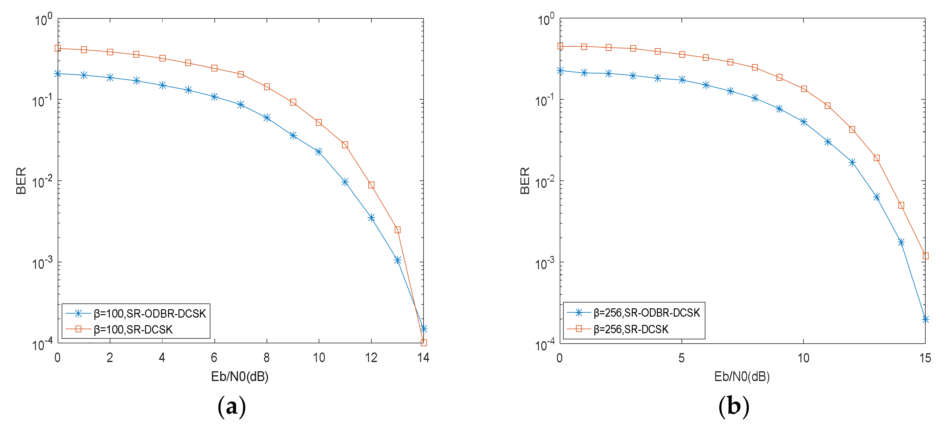
Figure 10 is the error performance comparison chart of the DCSK system and SR-ODBR-DCSK system. As is shown in the figure, when the semi-spread spectrum factor is equal to 100 and 256, the error performance of the SR-ODBR-DCSK system is better than that of the DCSK system.
The above simulation is only aimed at comparing the error performance of the two systems. The error performance comparison of the four systems is analyzed below.
Figure 11 shows the comparison of the error rates among the DCSK system, SR-DCSK system, ODBR-DCSK system, and SR-ODBR-DCSK system with the Gaussian white noise channel. It can be seen from the diagram that when the semi-spread spectrum factor is equal to 100, the error rate of the ODBR-DCSK system is the highest, and the error performance of the DCSK system and SR-DCSK system is similar. The error performance of the SR-ODBR-DCSK system is better than other systems. When the semi-spread spectrum factor is equal to 200, the error performance of other systems is worse than that of the SR-ODBR-DCSK system. When the signal-to-noise ratio is greater than 13 dB, the BER performance of the DCSK system is better than that of the SR-ODBR-DCSK system.
Figure 12 shows the relationship between the number of semi-spread spectrum factors and the bit error rate of the SR-ODBR-DCSK system and DCSK system when the signal-to-noise ratio is 10 dB in the Gaussian white noise channel using the circle mapping with the initial value of 0.6. Overall, with the increase in semi-spread spectrum factors, the bit error rate performance of the two systems first improves and then deteriorates. When
, the BER performance of the DCSK system is better than that of the SR-ODBR-DCSK system, but when
, the performance of the two systems is almost the same. When there is an intersection of about
in the diagram, it is obvious that the error performance of the DCSK system is better. The SR-ODBR-DCSK system has better BER performance when it is greater than this intersection point.
5. Conclusions
In this paper, an SR-ODBR-DCSK scheme is established to improve the energy efficiency and data transmission rate of the differential chaotic shift keying system. Based on the system of SR-DCSK, the modulation technology generates two orthogonal chaotic signals by using the orthogonal characteristics of the chaotic signal acting on the Walsh function and modulates the continuous two-bit data information respectively to realize the simultaneous transmission of two signals so as to improve the transmission rate twice on the basis of the original channel. Furthermore, the influence of four typical discrete chaotic mappings on the system is explored, and the simulation is carried out from three aspects replication number P, chaotic mapping type, and semi-spread spectrum factor. The simulation shows that the error performance is better when the number of reference signal replication P is 2. Four typical discrete chaotic maps have little effect on system performance under the same conditions. Different numbers of semi-spread spectrum factors will result in different BER performances. At the same time, the SR-ODBR-DCSK system is compared with the ODBR-DCSK system, SR-DCSK system, and DCSK system. It is found that the SR-ODBR-DCSK system has better error performance and high energy efficiency under the same conditions. Currently, we have studied the software simulation of the SR-ODBR-DCSK scheme, and in the future, we hope to implement the work of chaotic communication signal generation and modulation scheme using the FPGA hardware platform. SR-ODBR-DCSK system is promising and demonstrates great potential for the future of high-data-rate communication systems.


