1. Introduction
The use of chaos generators in the development of communication systems has been studied since the 1990s. One of the main advantages of chaotic communication systems is increased security [
1]. When chaotic oscillations are used as a carrier signal, it is difficult to detect its presence and decode the information, as it is difficult to predict the characteristics of the chaotic signal. The use of chaotic synchronization in communication schemes with coherent detection increases security even more, as it requires having a chaos generator with identical parameters and design at the receiver to synchronize and demodulate transmitted data bits [
2]. In addition, a chaotic signal is difficult to intercept, and it has relatively good resistance to multipath propagation and targeted interference [
3]. These properties of chaotic systems make them promising and interesting for academic studies and secure communication applications.
Several chaos generators, such as the Chua circuit [
4] or the Sprott circuit [
5], were originally based on an analog electronic circuit. They were based on resistors, capacitors, coils, operational amplifiers, bipolar transistors, and diodes to obtain and maintain nonlinear circuit oscillations in chaotic mode. Their chaotic behavior can be precisely mathematically described using relatively simple ordinary differential equations (ODEs).
The practical application of analog chaos generators in the design of communication systems raises several problems, such as component nominal value drift due to changes in temperature, relative humidity, supply voltage, and other environmental and operating conditions. Analog chaos generator parameter variations during the operation cannot be effectively compensated. Such variations of the system’s parameters make the chaotic synchronization task quite challenging, as it requires two chaos generators with identical parameters, coupled together in an appropriate way. Additionally, there is no option to control the initial states of analog chaos generator state variables. These issues have motivated some researchers and engineers to find alternative ways to implement dynamic chaos generators. One of the approaches is using a discrete implementation in field-programmable gate array (FPGA) technology. FPGA allows, with a certain approximation, implementing a dynamic chaos generator in a discrete environment by synthesizing a fully determined system that is free of the problem of component drift and has the potential for high throughput and computational power. In addition, an FPGA enables rapid, highly flexible prototyping with hardware description language and fast real-time parallel data processing using pipelining. These features can be effectively utilized to develop a chaotic FPGA-based communication system.
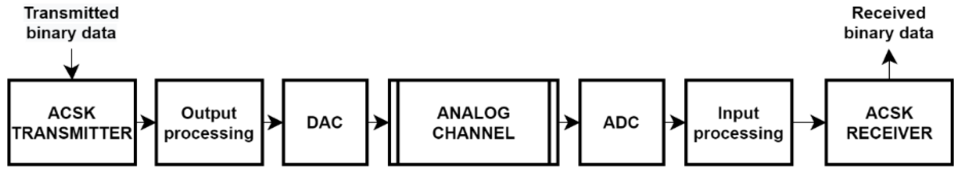
The FPGA-based ACSK communication system prototype, developed within the present study, includes digital and analog parts. The digital part is implemented on FPGA and contains an ACSK modulator, a demodulator, and transmitted and received signal processing units. At the same time, transmission between the transmitter and receiver is analog, using a digital-to-analog converter (DAC) and analog-to-digital converter (ADC). In addition to the FPGA prototype, a verified Simulink mathematical model of the communication system digital part was developed, which was used to compare the performance of the prototype and its nodes with the simulation.
This study proposes an FPGA-based prototype and a Simulink mathematical model of the ACSK communication system. The operation accuracy of the prototype and model is analyzed. The study of noise immunity of the ACSK system in the AWGN channel case is performed and represented in the form of BER analysis. The main goal of this study is to demonstrate the proof of concept prototype of a novel chaotic communication system implemented on FPGA. The main novelty aspects of the present work involve:
A modified Chua circuit chaos generator, error feedback chaotic synchronization, and a novel communication system with ACSK modulation are, for the first time, developed in the discrete format applicable for hardware implementation in an FPGA;
An accurate, verified Simulink mathematical model of the digital part of the proposed communication system prototype is developed;
The developed communication system is described in VHDL language, implemented on FPGA, and successfully tested.
This paper is organized as follows. A review of the literature and a comparison of existing implementations of chaotic systems based on FPGAs and the proposed system is carried out in
Section 2.
Section 3 describes the general structure of the communication system, including the chaos generator, chaotic synchronization, and ACSK modulation.
Section 4 explains the design flow and digital implementation structure of the system prototype and signal processing applied to the transmitted and received signals.
Section 5 describes a study of communication system noise immunity.
Section 6 provides conclusions.
2. Literature Review
The rapid development of FPGA technology began in the 21st century when it became widely available: the price decreased, and the number of logic elements and functionality increased. It became possible to use FPGAs to develop novel solutions and improve existing technologies, including chaos generator-based communication systems [
6].
Demand for new, well-protected communication systems in a variety of applications continues to grow today. Still, the analysis of several scientific articles about FPGA-based chaos generators and chaotic communication systems (summarized below) reveals that their number is relatively low compared to chaotic communication systems based on other analog and digital bases [
7]. The lack of research on the application of FPGAs in chaotic communication can be explained by the relatively recent development of FPGAs and the complexity of low-level hardware programming required for FPGA configuration. Therefore, it is essential to make an advance on the topic of FPGA-based chaotic communication systems to reveal their advantages, disadvantages, and potential applications.
Some authors who have implemented dynamic chaos generators in FPGA are listed in
Table 1. In most cases, the author’s studies are limited to chaos generator implementation, but four of them also include chaotic synchronization between master and slave chaos generators. The FPGA-based chaotic systems comparative analysis parameters are chaos generator type, chaotic synchronization method, the maximal clock frequency of the FPGA prototype, ODE discrete solving method choice, and bit width of the system. Authors emphasize the potential advantages of FPGA compared to analog implementations, such as higher stability, fast parallel processing, and low power consumption.
Table 2 presents the overview of the existing studies about FPGA-based chaotic communication systems, which is the following and more advanced step after implementing chaos generators and synchronization. The analyzed parameters are the same as in the studies listed in
Table 1, plus the modulation technique used for the communication.
One of the first articles on this topic [
23] describes a chaotic communication system for encoded image transmission. The system uses a modified FPGA-implemented Chua chaos generator for information encoding and classic Pecora-Carroll chaotic synchronization [
24] for coherent demodulation. Another article [
25] describes the FPGA implementation of a generalized chaotic Lorentz system, which is used to design a communication system in which chaotic synchronization occurs with a controlled chaos generator in the receiver, implemented on a personal computer. Reference [
26] is devoted to an FPGA-based communication system using a novel chaos generator and the chaotic synchronization method with the Hamiltonian form and the observer approach [
27]. In another article [
28], four modifications of a simple chaos on-off keying (COOK) communication system with a Sprott chaos generator were developed. Their performance was tested in three implementation environments—FPGA, analog circuits, and Simulink mathematical model. By comparing bit error ratio (BER) graphs, the authors concluded that the performance of the FPGA-based communication system in the white noise channel is better than the performance of the analog counterpart. In another study [
29], the authors propose an FPGA-based communication system using synchronization between Rossler chaos generators. It is noteworthy that the prototype’s maximum clock frequency and throughput were significantly increased by reducing the bit width from 32 to 19 bits. Reference [
30] contains a study covering and comparing several chaos generators and various chaotic synchronization methods, including the open-plus-closed-loop (OPCL) [
31], and several discrete approaches for solving ODEs.
Table 2.
Summary of chaotic communication systems implemented in FPGA.
Table 2.
Summary of chaotic communication systems implemented in FPGA.
| Paper | Chaos Generator | Chaotic Synchronization Method | Modulation | FPGA Prototype max Clock Frequency, MHz | ODE Discrete Solving Method | Max Through-put, Gbps | Bit Width of a System (Integers with Sign + Fraction) |
|---|
| [23] | modified Chua | Pecora-Caroll | Author’s, digital algorithm | not mentioned | Forward Euler | not mentioned | 32 (not mentioned) |
| [25] | Lorenz | author’s | Chaotic masking | not mentioned | Not mentioned | not mentioned | 27 (not mentioned) |
| [26] | author’s | Hamilton forms | Chaotic masking | 275.71 | Forward Euler | 5.24 | 19 (15 + 4) |
| [28] | author’s and Sprott | none | COOK | not mentioned | not mentioned | not mentioned | not mentioned |
| [29] | Rossler | Pecora-Caroll | Chaotic masking | 70.9 | Forward Euler | 2.85 | 19 (10 + 9) |
| [32] | author’s | Hamilton forms | Chaotic masking | 1 | Forward Euler | not mentioned | 28 (4 + 24) |
| [30] | Sprott | Pecora-Caroll, Hamilton forms, OPCL | Chaotic masking | 116.4 | Forward Euler, trapezoidal, RK-4 | 3.26 | 28 (7 + 21) |
| present | modified Chua | error linear feedback | ASCK | 76 | Forward Euler | 1.06 | master: 14 (6 + 8),
slave: 17 (9 + 8) |
To analyze the parameters of overviewed FPGA-based chaotic system implementation studies, listed in
Table 1 and
Table 2, their advantages and disadvantages are discussed below.
In many cases, research is carried out with well-known chaos generators (Lorenz, Chua, Sprott, Rossler, and others), although new chaos generators proposed by the authors are sometimes used. The approach of FPGA employment makes it much easier to implement relatively complex chaos generators than it can be done in an analog circuit. Chaos generators may be of different complexity, signal parameters, number of state variables, and chaotic synchronization capabilities. However, any generator can be implemented in FPGA and utilized to develop a secure communication system. What authors demonstrate in their studies is the approach and methodology of such implementation, which can also be applied to other chaos generators.
For chaotic synchronization methods within the studies, the classical Pecora-Carroll [
24] or more advanced Hamiltonian forms with an observer approach [
27] are used most often. At the same time, the synchronization error feedback method [
33] was used only in one overviewed study. The choice of synchronization method generally comes from an acceptable trade-off between synchronization complexity and quality. For example, Pecora-Carroll synchronization is the first discovered and simplest chaotic synchronization. In contrast, the synchronization error feedback method requires a more complex approach but ensures faster and more stable chaotic synchronization between identical master and slave chaos generators.
The overviewed communication systems mostly used chaotic masking modulation [
7], the simplest method for coherent detection that uses chaotic synchronization. In chaotic masking, a relatively weak data signal (analog or digital) is added to a stronger chaotic signal and transmitted. The received signal is used to recreate a synchronized copy of the chaotic part of the received signal, which, by subtraction from the received signal, makes it possible to extract the added information signal. The simplicity of this method makes it popular, but it has several disadvantages—low noise resistance, the data signal itself weakens chaotic synchronization, and low data transmission security. Another chaotic modulation mentioned in
Table 2 is COOK, used in the noncoherent detection communication system that does not utilize chaotic synchronization. In COOK, binary data symbols are modulated simply by turning the transmission on or off. The method has some advantages in terms of higher speed and lower multipath propagation impact on transmission but provides virtually no data protection.
For numerical solving of ODEs, the forward Euler method [
34] is used most often because of its simplicity. It is discussed in more detail in
Section 4 of the present paper. The fourth-order Runge-Kutta (RK-4) method [
32] is more advanced and complex for FPGA implementation, but it provides a more precise ODE solution and is sometimes preferred. Some chaos generators may be more sensitive to the accuracy of their ODEs solutions than others due to the complexity and operation mode. Using the forward Euler method does not guarantee convergent ODE solutions, a more accurate method such as RK-4 is necessary.
The maximum operational clock frequency of the FPGA, at which the implementation of the chaos generator works without errors, varies from 1.00 MHz to 275.71 MHz in different experimental studies, depending on the system’s complexity. If the system clock frequency is above a specific limit, metastability issues in logical element circuits on the FPGA chip may become unavoidable, making system operation invalid. General approaches to increasing the maximum clock frequency involve maximizing pipelining, minimizing the amount of asynchronous data processing between registers, reducing the bit width of data signals, and using logical or arithmetical bit shift instead of division or multiplication by a constant value [
35]. However, the design complexity of a specific chaos generator significantly impacts this parameter so that general design optimizations may have little effect on the maximum operational clock frequency available for a specific chaos generator FPGA implementation.
The throughput rate is defined as the number of bits per unit of time. In a digital system, the maximum throughput is calculated by multiplying the minimum number of bits in the signal bus with the maximum clock frequency. For the analyzed studies, the throughput varies from 0.81 to 5.77 Gbps. This parameter helps to evaluate the performance of the digital implementation of the system, while it mainly depends on the achievable maximum clock frequency.
The signal bit width of the chaos generator FPGA implementations in the overviewed studies is between 10 and 64 bits, with different fixed-point locations. The number of bits needed for the integer part of chaotic signal numeric values can be chosen from the consideration that 2n−1 < k < 2n, where k is the maximal numeric value of any signal within the system and n is the number of bits required to represent the value. Choosing the number of bits for the fractional part of chaotic signals does not have well-defined and straightforward rules. Increasing the number of bits for the fractional part will increase the accuracy of chaotic solutions and the number of possible values that a chaotic signal can represent. Still, it will decrease system maximal clock frequency and consume more hardware resources for signal processing. Therefore, a moderate number of bits for the fractional part should be chosen, depending on the required accuracy and available resources. The actual number of bits for signals within the system may vary from the main number required to maintain the accuracy of calculations within system nodes.
When comparing the present work and the literature by the same parameters, there are several different and common aspects:
The present system uses a specific modified Chua circuit chaos generator and error feedback chaotic synchronization method. This chaos generator is not used in previous studies, while error feedback chaotic synchronization is implemented in FPGA within one research;
For modulation, the proposed communication system uses antipodal chaotic shift keying (ACSK), which is more advanced than chaotic masking and has not been used in any overviewed studies about FPGA-based chaotic communication systems;
For ODE numerical solving, the present study also uses forward Euler, which provides sufficient accuracy and stability of solutions;
The maximum clock frequency of the FPGA in the prototype is equal to 76 MHz, but the design utilizes a 50 MHz clock that is provided by the FPGA onboard peripheral resources;
Concerning signal fixed-point bit widths, 14 bits for the transmitter and 17 bits for the receiver are used (with one bit for the sign), allocating 8 bits to fractional values;
The maximum throughput for master chaos generator output is 1.06 Gbps. This is mainly determined by the maximum clock frequency limitations. The chaos generator maximal throughput can be increased by redesigning the structure of the generator’s digital implementation and performing pipelining on the addition and the discrete integration. However, such an approach would increase the hardware resource usage and the design complexity. The present study assumes that the optimization level is sufficient to demonstrate the proof of concept for FPGA implementation of the novel ACSK communication system.
The chaotic systems implemented on FPGA are also compared by the hardware resource usage, as shown in
Table 3. Only those research papers are listed where at least partial resource usage information is provided. Resource usage numbers generally represent chaos generator implementations, sometimes with simple additional units used in different studies. Configurable Logic Block (CLB) is a Xilinx brand FPGA basic logic block, while Adaptive Lookup Table (ALUT) is an Altera (presently owned by Intel) brand FPGA basic logic block. They consist of registers, lookup tables (LUTs), multiplexers, full adders, carry chain logic, and other basic digital elements depending on the FPGA brand and series. These differences complicate resource usage comparison between different FPGA, but they nevertheless provide good reference data for the estimation of design complexity. Embedded memory is sometimes used for buffers necessary for processing delay or information storage when registers and LUTs are insufficient due to the size of information. The registers (flip-flops) are the key elements that synchronize signals within FPGA to the clock and store the signal values until the next clock cycle. An increase of the registers in the design implementation introduces small additional latency but allows higher clock frequencies to be used. Moreover, digital signal processing (DSP) blocks are separate hardware units within FPGA chips that provide support for common fixed-point and floating-point arithmetic operations, most commonly—multiplication. The number of DSP blocks in FPGA chips is typically small compared to logic blocks or registers, so reducing the number of used DSPs in the design implementation is a good practice.
The current FPGA implementation of modified Chua’s circuit chaos generator uses 564 ALUTs, which is less than most other implementations, indicating relatively low design complexity. Embedded memory is not employed in the present design, but 84 registers are used, which is a small amount compared with other implementations and can be increased for future optimization tasks. FPGA registers are single-bit, so 84 registers for 14-bit signals can be interpreted as six 14-bit registers. Finally, 4 DSP multipliers are used for four weight coefficients in the chaos generator’s output signal design, which is less than in most other designs and can be reduced to zero by further optimization and replacing multiplication with a combination of bit shifts and adders.
Table 3 summary of resource usage for chaos generators implemented in FPGA.
The main advantage of the proposed FPGA-based chaotic communication system over others is the ACSK modulation method, which is a potentially more secure method for data transmission than chaotic masking or COOK because it uses chaotic synchronization.
4. Communication System Prototype Structure
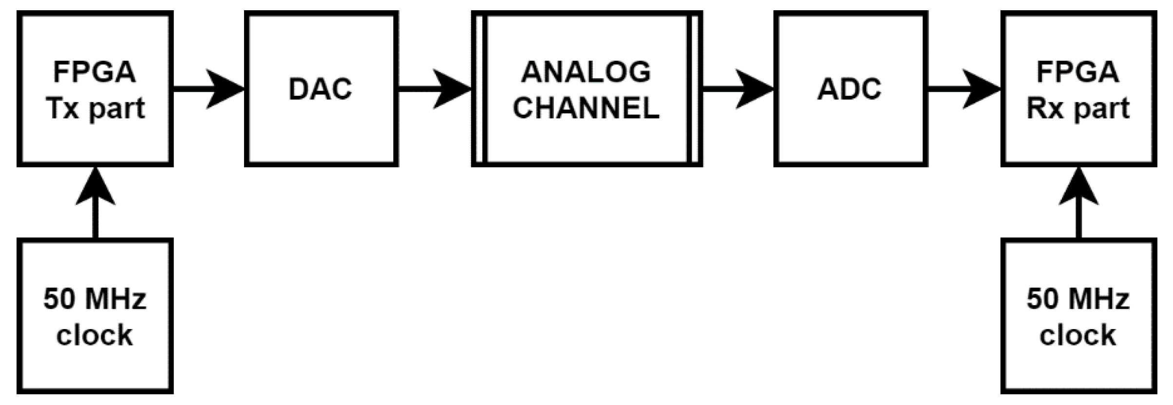
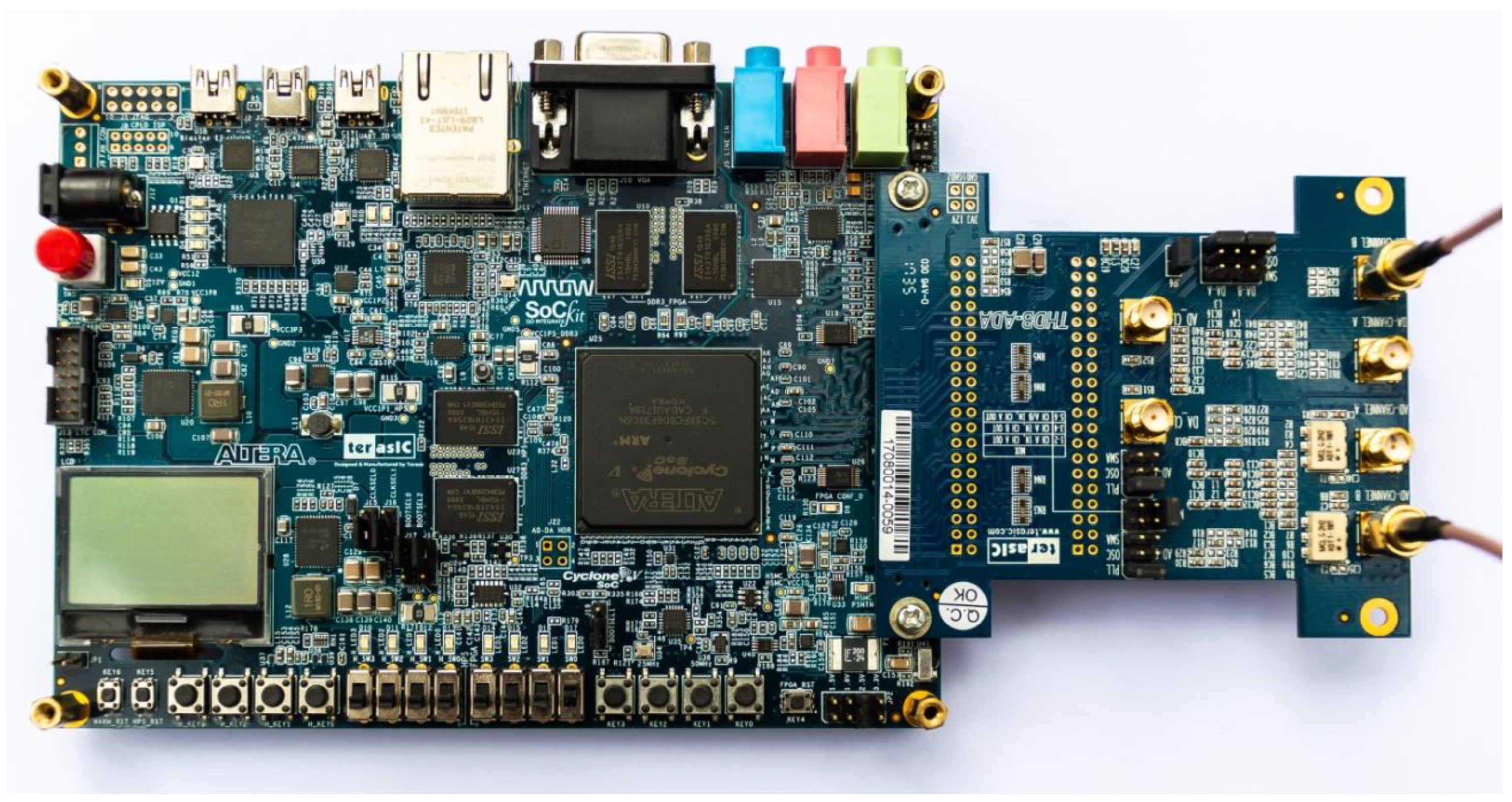
This section describes the FPGA implementation of the ACSK receiver and transmitter. As shown in
Figure 7, the prototype setup consists of Altera Cyclone V 5CSXFC6D6F31C6N FPGA digital transmitter and receiver, clocked by the onboard 50 MHz clock source, and analog channel with AD9767 DAC and AD9248 ADC. A further focus of this section is limited to the digital implementation of transmitter and receiver, where modulation, demodulation, and signal processing are done.
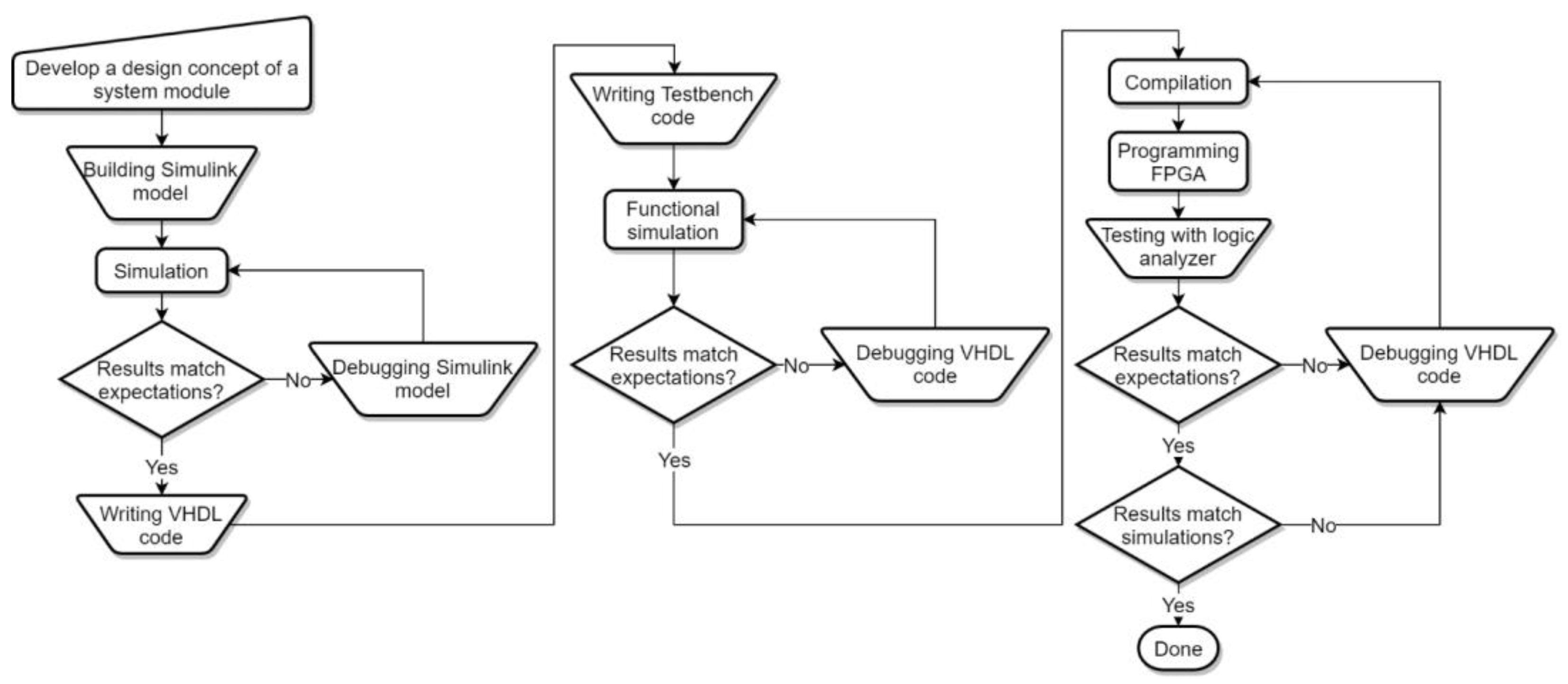
The design of an FPGA prototype is carried out in several stages, starting from the concept and ending with the hardware implementation. System modules—e.g., chaos generator, filter system, automatic gain control, and average value estimation—are first developed and tested separately from other modules, incrementally connecting them together. The main stages of the design flow and methodology are shown in
Figure 8.
At the start, a design concept is developed, considering the system module’s desired functionality, parameters, and structure. The Simulink model is then developed that uses only basic digital elements and fixed-point signals to closely match the module design to be implemented in the FPGA.
Once the Simulink model has been validated and verified, the module design is described using the VHDL hardware description language, manually defining the interconnection of adders, registers, multipliers, and other elements. Editing, automated analysis, and synthesis of modules described in VHDL files is performed in the Quartus Prime software. A testbench file is written for each module to perform a functional simulation of the synthesized FPGA design. The testbench file helps test the VHDL modules separately by providing appropriate input signals to the synthesized module and checking the output signals. The functional simulation is performed using the ModelSim software and verifies the functionality of the designed module without evaluating the effect of the actual hardware implementation in FPGA.
When the functional simulation step is completed, Quartus performs a full compilation to create a binary file used to program the FPGA chip. The main project setup parameter required for successful compilation is selecting the exact target FPGA device, in this case—Altera Cyclone V 5CSXFC6D6F31C6N. Additionally, any FPGA pins used for peripheral devices and interfaces (such as clock source, buttons, LEDs used, etc.) must be specified precisely in the Quartus Pin Planner settings before the compilation. Most of the other Quartus compilation settings are used in the default configuration.
During a full compilation, automated analysis of the VHDL code and synthesis of digital implementation structure is performed at the beginning. Then, fitting and assembling operations are done by Quartus. The fitting determines the placement of all digital logic elements on the FPGA chip and the signal routing logic. The assembling generates a binary programming file used to program the FPGA chip.
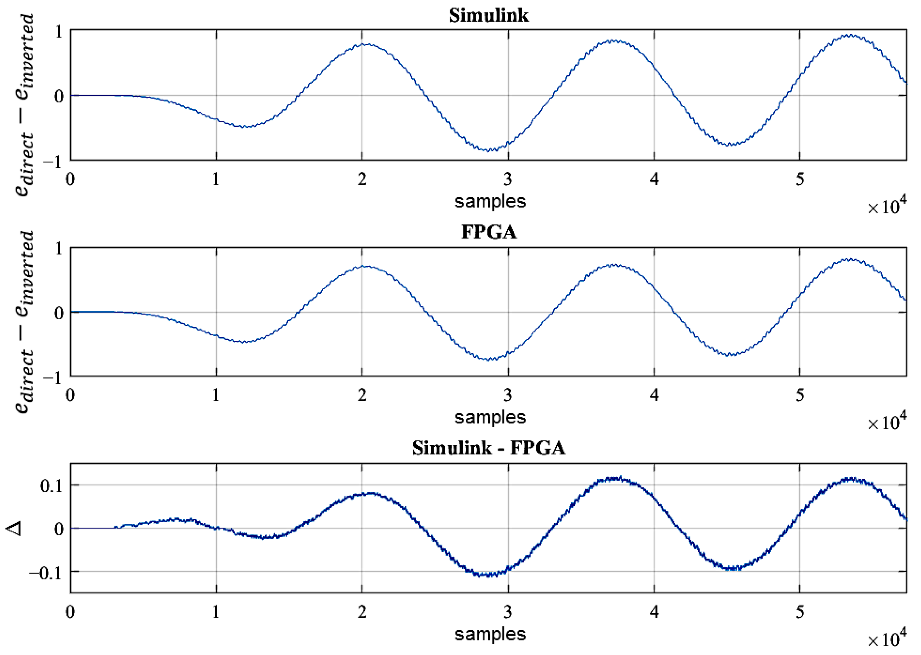
Quartus provides a built-in Signal Tap logic analyzer tool that can be configured before the compilation to track specific signals to perform on-chip verification and debug of an implemented and programmed module. Signal Tap can visualize monitored signals as the time diagrams or export the recorded binary data for external processing. In the final stage of the module design verification, module output signals are recorded from the programmed FPGA and exported to MATLAB software, where they are compared with module outputs generated by simulation of the Simulink model.
The described approach is used not only for individual modules of the system but also for their appropriate combination. At the final stage of the communication system implementation, it is used for the entire prototype.
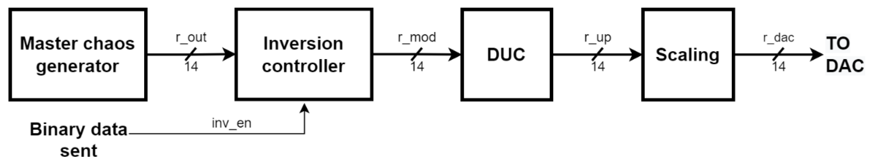
4.1. Transmitter
The transmitter structure is shown in
Figure 9. The main module is the master chaos generator that synthesizes the discrete chaotic signal to be inverted or not inverted, depending on the transmitted bit value, which is the essence of the ACSK modulator. The ACSK-modulated chaotic output signal is prepared for analog transmission by two processing steps: digital up-conversion (DUC) and scaling. The implementation of the chaos generator and processing units in the transmitter are described further.
4.1.1. Chaos Generator Implementation in Field Programmable Gate Array
The FPGA is intended to implement discrete digital systems, while the chosen chaos generator is a continuous dynamic nonlinear system. Implementing a chaos generator in an FPGA requires two considerations: the choice of a discrete ODE solution method and the choice of a binary numeric data format for signals.
The forward Euler method [
32] is used for solving ODE, which is simple, and therefore, consumes fewer physical FPGA resources than other methods and provides convergent solutions. The following expression can describe the forward Euler numerical ODE solution method:
where
yn is the present system state variable,
yn+1 is the next estimated value, h is the solution step size, and
f(
yn) is the increment function. The solution converges to the actual value as step size approaches zero. Solution step size
h = 1/1024 is chosen in the system design, which provides acceptable precision, and is suitable for simple FPGA implementation. It has been assessed that with step size
h = 1/256 system, ODE solutions diverge because solution approximation precision becomes insufficient.
Applying the forward Euler method, (1) can be expressed as:
For a discrete numerical representation of system signals in the transmitter, a 14-bit signed two’s complement fixed-point format is used, where 8 bits represent the fractional part, and 5 bits are the integer part and sign. In the receiver, signal data width is generally equal to 17 bits (8 bits for the fractional part, 9 bits for the integer part and sign), with some exceptions inside signal processing modules.
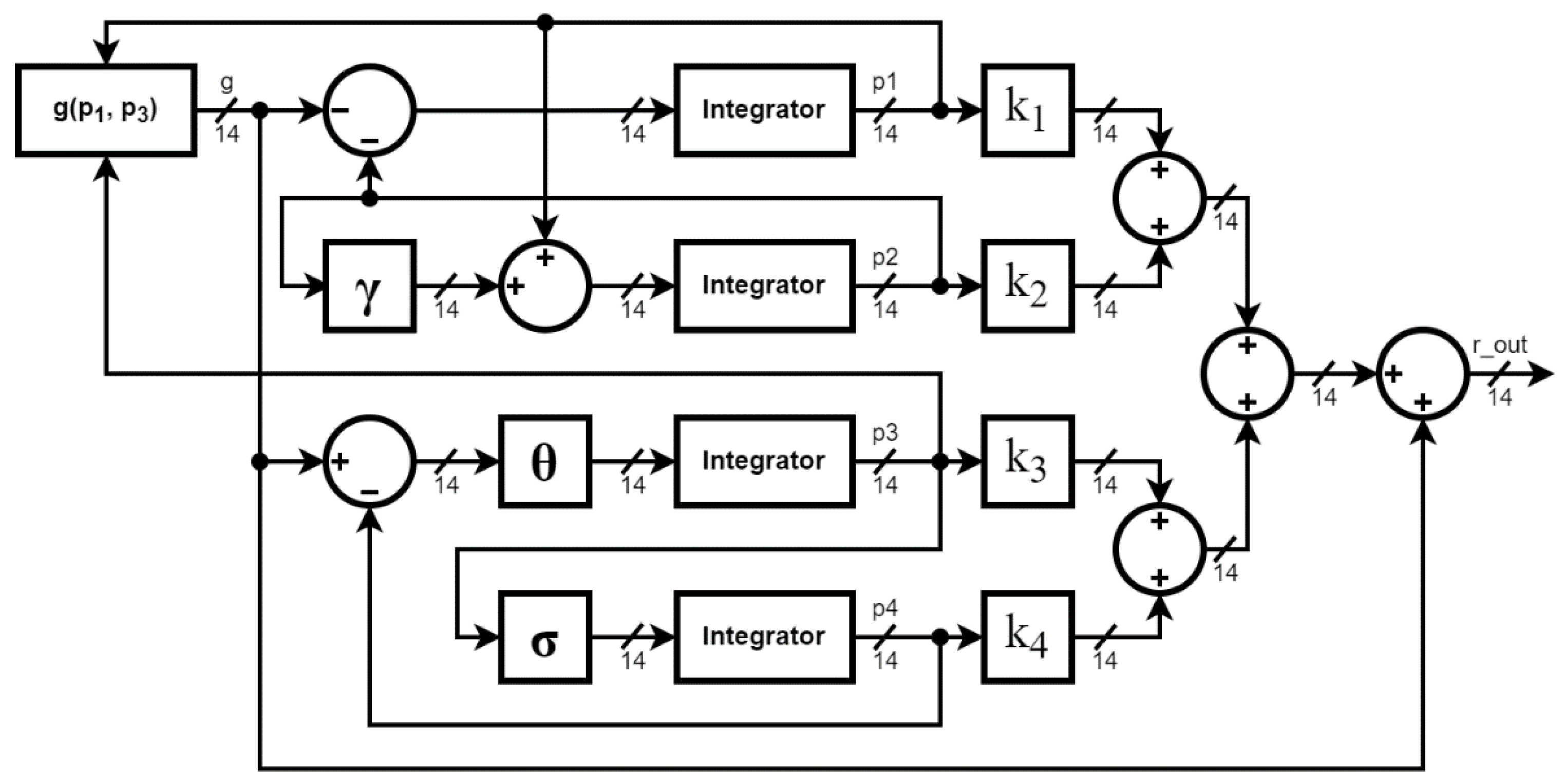
The chaos generator equations (7) were implemented by separately designing and interconnecting mathematical units as shown in
Figure 10, where integrator is the forward Euler ODE solution unit, which consists of adders and registers, and works according to Equation (6), with increased bit width within the integrator and rounding at the output. The piecewise linear function
is designed according to the Equation (2) and consists of three adders, a comparator, and a multiplexer, while bit width changes and rounding are not required for its implementation. Now, coefficients
θ,
σ, and
γ are constant and do not require a digital multiplier to implement. For instance, multiplication by 0.5 for
γ coefficient equals a single logical bit shift to the right; therefore, division or multiplication by power of 2 requires no hardware resources. Multiplication by 1.5 for
σ coefficient uses one adder; its inputs are the signal to be multiplied and its right-shifted (by 1) copy. Multiplication by 10 for
θ coefficient is implemented similarly, using one adder and two signal bit left-shifts (by 1 and by 2)—one of the shifted signals is supplied to the first adder input, and the other is on the second adder input.
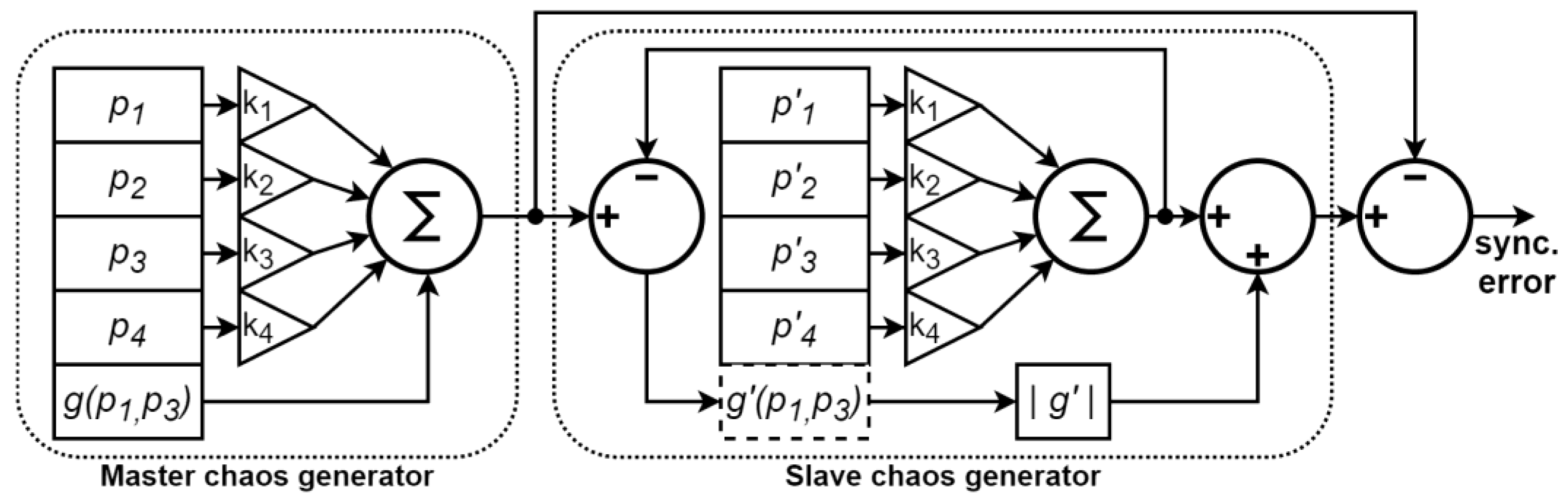
On the output part of the master chaos generator, state variables
p1–p4 are multiplied by weight coefficients
k1–
k4 accordingly, using digital multipliers of FPGA DSP blocks. As these coefficients are constant, it is possible to optimize their value and implementation in future prototype designs to avoid the use of multipliers. Weight coefficients are represented in 14 bit-width formats, the same as the multiplier input signals. When two 14-bit fixed-point signals are multiplied, the product is represented by 28 bits, where the number of bits for both fractional and integer parts is doubled. To reduce the number of the product bits back to 14, some rounding is performed by taking only half of the bits before and after the radix point position. Weighted signals of state variables are summed together and with the piecewise linear function
g(
p1,
p3), using four adders to produce the chaotic output signal, as shown in
Figure 10.
Registers are only used in the integrators so that one clock period would correspond to one iteration of solving ODEs according to the Forward Euler algorithm. This simplifies design, but limits the maximum clock frequency at which the prototype can produce valid solutions, since binary adders take a finite time to complete the carry chain during calculations. Increasing the number of registers between asynchronous digital parts would increase the pipelining effect and maximal clock frequency limitations; however, this will complicate the ODE discrete solving algorithm and increase hardware resource usage.
4.1.2. Signal Processing before Transmission
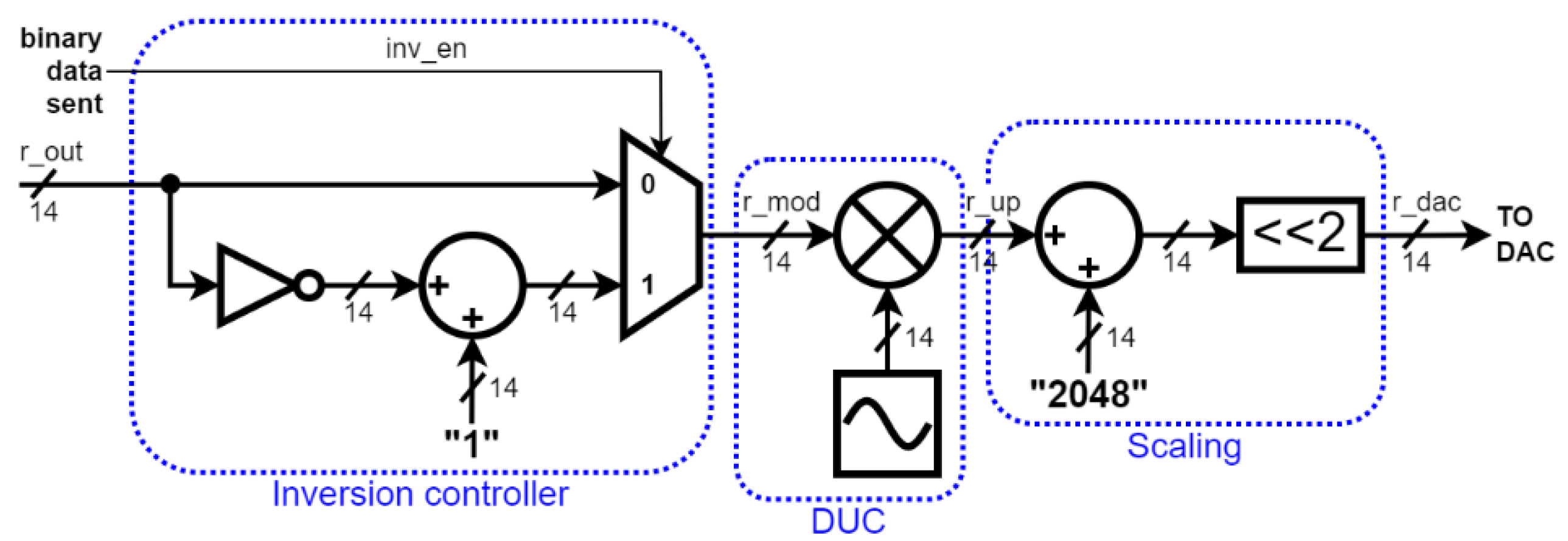
Figure 11 shows the structure of modulation and processing unit FPGA implementations—inversion controller, DUC, and scaling.
The arithmetic inversion of digital data values stored in fixed-point two’s complement format is performed in two simple steps—bits are bitwise inverted, and a 1 is added. A multiplexer is used to select which type of chaotic signal is passed further, direct or inverted, selected by the value of binary data transmitted.
In DUC, the chaotic baseband signal is multiplied by 793.65 kHz digitally synthesized harmonic waveform (with amplitude equal to 1), moving the transmitted signal to an approximate frequency range between 579 kHz and 1009 kHz. Since a 50 MHz clock is used as a sampling frequency in the FPGA prototype, there was no need for up-sampling within the DUC module since the intermediate frequency of 793.65 kHz is significantly below the Nyquist frequency.
The harmonic waveform signal is implemented using a LUT filled with 64 samples (in 14-bit fixed-point format) of one sine period and a 6-bit phase counter. The free-running counter provides an instantaneous phase value that selects a LUT entry for the sine generation. It uses multiplexers to select the appropriate LUT entry and an adder for the counter. Multiplication of two 14-bit numbers results in a 28-bit product, from which only 14 bits are selected for the output, as previously mentioned.
Since the DAC interface supports straight offset binary (SOB) format input, the digital scaling unit adds DC bias to convert data into a 14-bit SOB format. Additionally, the signal amplification is done. The DC bias added is cancelled by the RF transformers after DAC, so it does not affect the transmission.
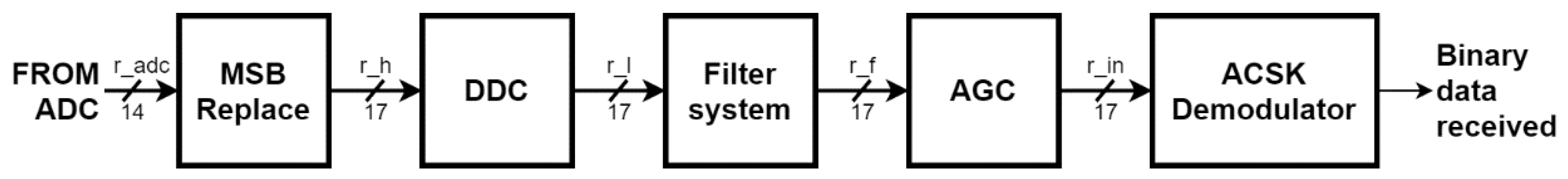
4.2. Receiver
The received signal must be processed before passing it to the ACSK demodulator. The 14-bit SOB format digital output signal from the ADC channel has an added binary offset value of 2
13, which needs to be cancelled. Thus, the MSB bit inversion removes the binary offset from the received signal by converting it to the signed two’s complement format. At the same stage of scheme data bus bit-width is expanded from 14 to 17 bits to prevent overflow in further processing stages. As shown in
Figure 12, further digital processing of the received signal includes converting the signal from the intermediate frequency to baseband with digital down-conversion (DDC), filtering, and adjusting the signal level with automatic gain control (AGC) unit. The processed signal is passed to the ACSK demodulator, where the transmitted bits are detected.
The implementation and structure of the DDC unit are similar to the DUC unit—the digitally synthesized harmonic waveform is multiplied with the input signal using a DSP multiplier. The only difference with DUC is that signals are 17-bit, including harmonic waveform. Therefore, the multiplication product is 34-bit large, and rounding is performed to provide 17-bit output. Mixing the input signal with the 793.65 kHz harmonic wave signal in DDC results in splitting the signal into the baseband and the double intermediate frequency (of 1587.30 kHz) components. The double-frequency spectral components are filtered out in the next processing step. The digital structure of the filtering system, AGC and ACSK demodulator units, is discussed next.
4.2.1. Filtering System
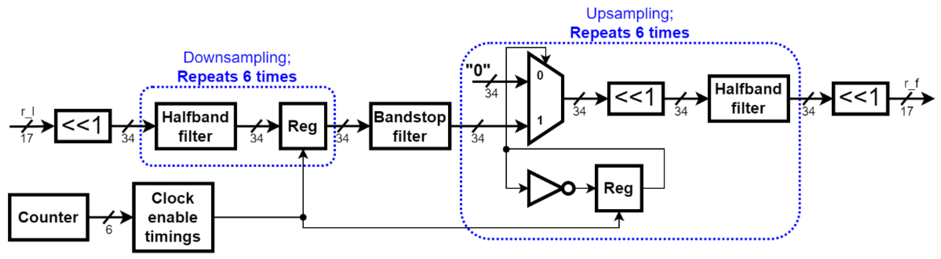
The filtering system provides immunity to channel noise by filtering the signal spectrum outside the frequency regions most essential for chaotic synchronization, below 6 kHz and between 90 and 215 kHz. The implementation of a single filter with two passband regions is possible, but it requires a high filter order and design complexity. Instead of using a single-filter approach, the filtering is done by connecting several filters with low order and simple design. It should be noted that all the sampling and signal frequencies described are valid for 50 MHz clock use for the FPGA prototype. Increasing the FPGA clock frequency proportionally increases the frequency of the chaotic signal.
The filter system design consists of down-sampling, bandstop filter, and up-sampling. Only two filters were designed and used in the current implementation—the sixth-order halfband lowpass IIR filter and twelfth order bandstop IIR filter. The cutoff frequency of the halfband filter is equal to 0.546 of the sampling frequency. The bandstop filter is used sequentially six times, and down-sampling by 2 is performed after each use. This way, the sampling frequency is down-sampled by 2 six times—from 50 MHz to 781.25 kHz. When the halfband filter is applied last time in this stage of the filter system, its actual cutoff frequency is 213.281 kHz, which is acceptably close to the desired value of 215 kHz.
The down-sampling makes it possible to use a much simpler bandstop filter to cut off frequencies between 6 and 90 kHz than it would be necessary at a 50 MHz sampling frequency. After the bandstop filter, a six-stage up-sampling by 2 is performed to return the signal sampling frequency to 50 MHz, at which point it needs to be further processed and used for chaotic synchronization. After every up-sampling stage, the signal is multiplied by 2 (using a single logical bit left-shift) to compensate for the energy loss in the baseband, caused by signal spectral division into two parts—at the baseband and the half of the new sampling frequency. The signal part, which is outside baseband frequencies, is filtered by the halfband filter at every stage.
The generalized structure of the filtering system’s digital implementation is shown in
Figure 13. Filtering is performed with doubled signal bus bit width (34 bits) to achieve a better calculation accuracy. The different sample rates are controlled by providing different clock enable signal rates for the registers, while all registers keep using the same clock signal. For example, to down-sample a signal by 2, the first down-sampling stage register is enabled only once per 2 clock cycles, the second down-sampling stage register is enabled once per 4 clock cycles, etc. Up-sampling is implemented in reverse order. A register with inverted loopback is used to control a multiplexer with a clock enable signal with a twice higher rate than the previous. The multiplexer divides every previous sample into two samples, giving the second sample value of “0”.
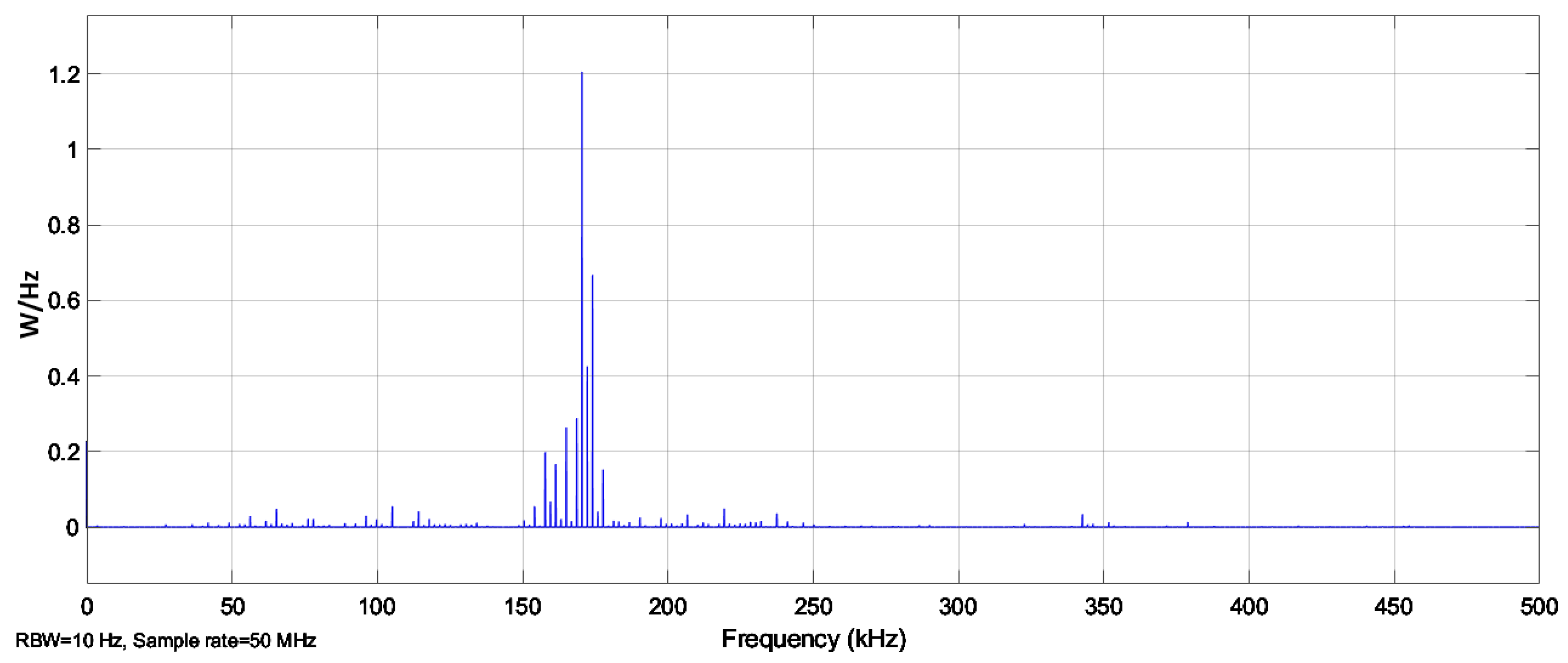
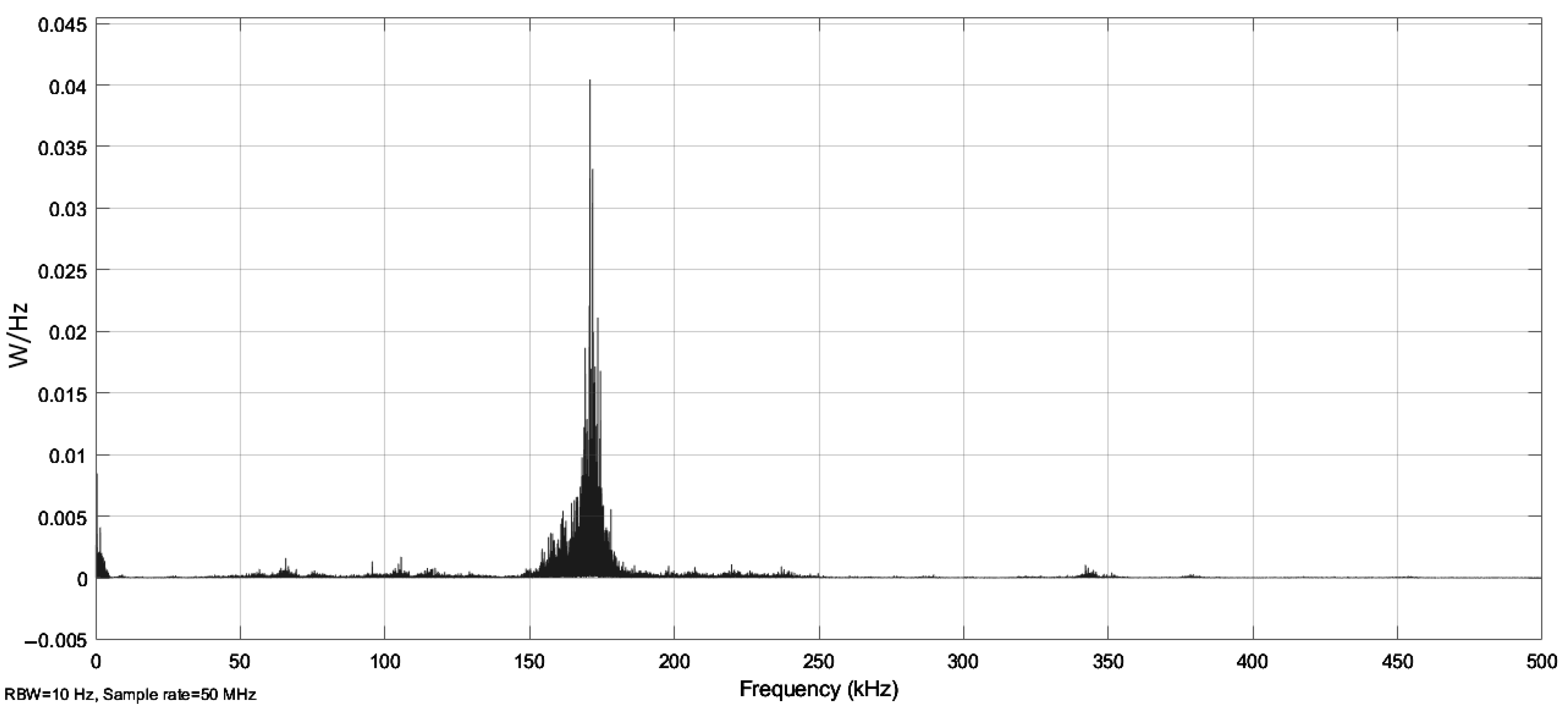
The baseband spectrum of the transmitter output chaotic signal, manipulated with random bit sequence, without any channel noise added, is shown in
Figure 14.
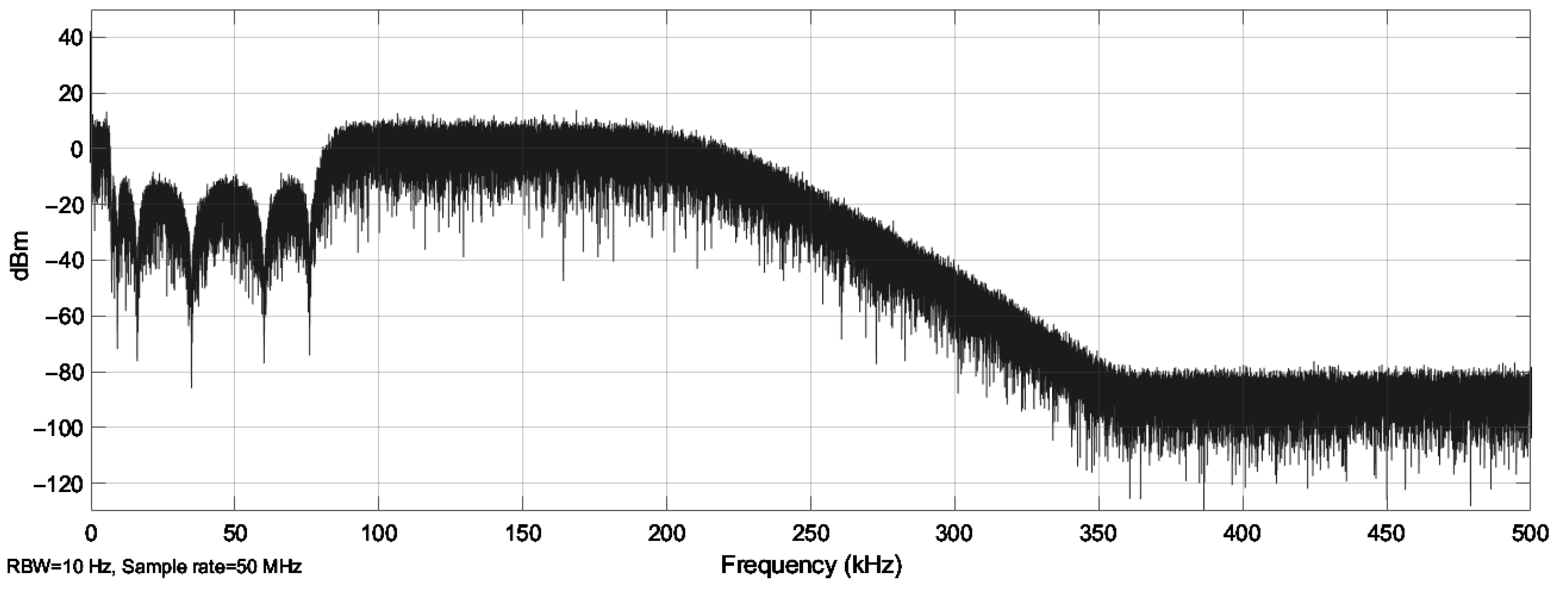
Figure 15 shows a frequency magnitude response of the whole filter system obtained by applying white additive Gaussian noise of power level 0 dBm in the Simulink mathematical model.
4.2.2. Automatic Gain Control
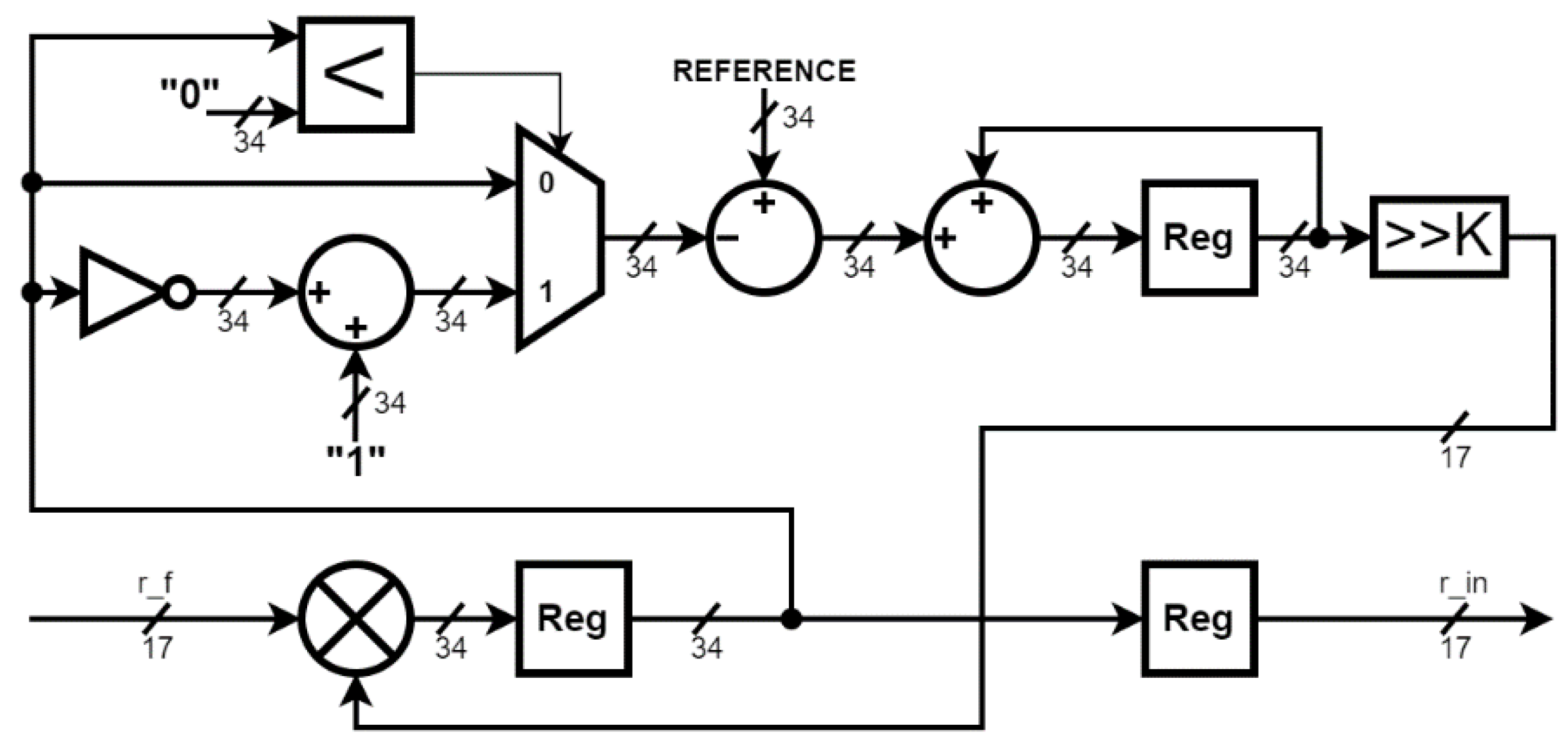
As the received signal and transmitter output signal levels may differ due to channel noise, attenuation, and other factors, an AGC unit is required to adjust the received signal gain to the estimated reference power. Thus, the signal power applied to the receiver slave chaos generators is close enough to the power level of the master chaos generator in the transmitter.
A feed-backwards type of AGC is implemented in the present prototype. As shown in
Figure 16, the incoming signal is multiplied by the feedback signal, obtained in the following way. Output signal absolute value is obtained using a comparator, an arithmetical invertor, and a multiplexer. The multiplexer selects an inverted signal value when the signal is below zero or a direct value when the signal is positive. The absolute value of the input signal is subtracted from the reference and passed to the gain accumulator. The reference is the RMS value of the modulated output signal of the master chaos generator, equal to 2.421. After the accumulator, the signal is divided by 2
K (using a logical bit right shift K times), closing the feedback loop. The choice of number K impacts the dynamic range and operating speed. These parameters were evaluated for K values from 10 to 17 and input signal power from 10 times smaller to 10 times greater than the reference power value. K value of 14 was chosen at which AGC performance provides an acceptable trade-off between dynamic range and speed. The data bit width at the input and output of the AGC is 17 bits. In the internal cycle, the bit width is increased to 34 bits to ensure that the value stored in the accumulator is represented with an acceptable total rounding error. The 34 bits represent twice the number of bits for the integer and fractional parts of fixed-point values, which is enough to represent any result of multiplying two 17-bit fixed-point binary numbers according to the rules of binary arithmetic.
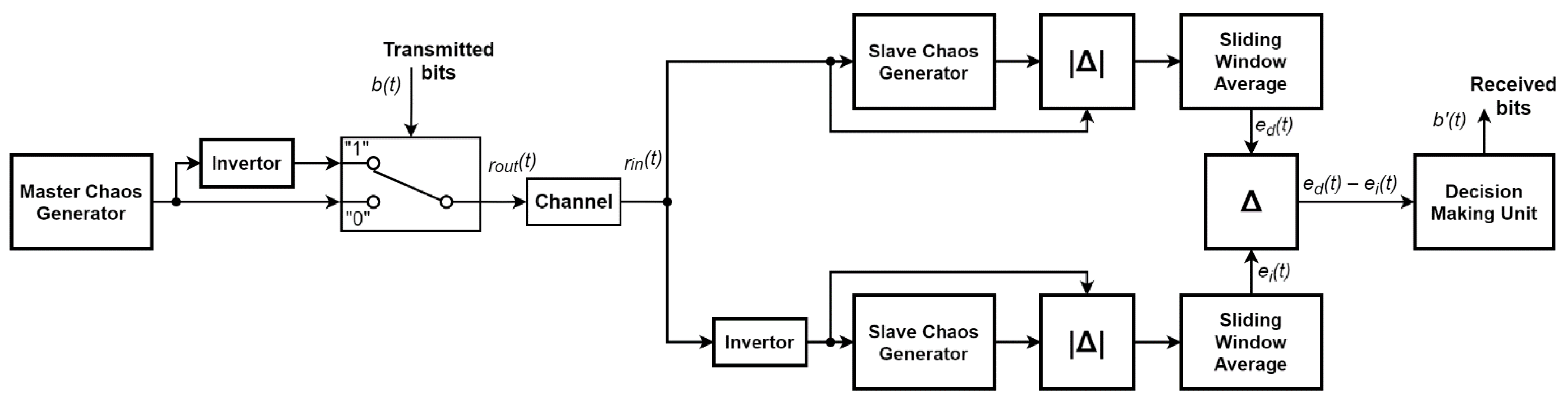
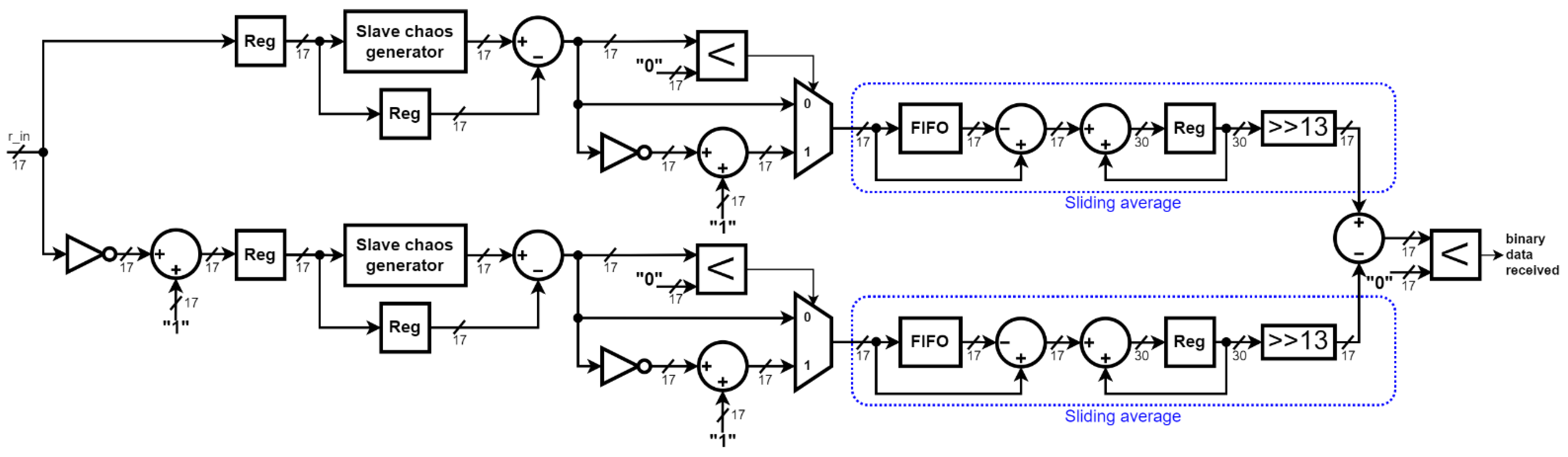
4.2.3. ACSK Demodulator
The general design and functionality of ACSK demodulator were previously discussed in
Section 3.3. The present subsection focuses on the digital implementation structure of the demodulator modules, which is shown in
Figure 17. The processed input signal is divided into two parts. One part is applied to one of the slave chaos generators without modifications, while the other part is arithmetically inverted before being applied to the second slave chaos generator.
The implementation structure of the slave chaos generator is mostly identical to the master chaos generator, with only a few differences:
The signal bus is 17-bit, as in most of the receivers—one of the reasons for this is that much higher signal values within the slave chaos generator can be observed when chaotic synchronization is not established, which is the desired operation in one of two generators during transmission;
Piecewise linear function
g(
p1, p3) is absent and is reconstructed by a negative loopback, as shown in
Figure 4;
The output signal uses the absolute value of the reconstructed piecewise linear function.
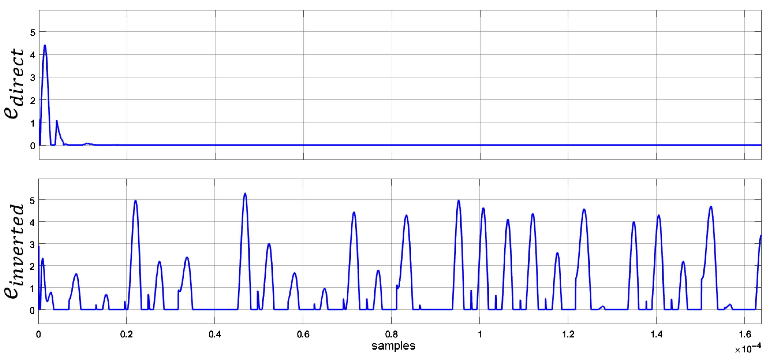
The input signal of each slave chaos generator is subtracted from its output to obtain a signal representing chaotic synchronization error. The absolute value of the error signal is then averaged over the 8192 (213) samples with a sliding calculation window.
Sliding average value calculation is implemented using a FIFO memory buffer that can store up to 8192 records of 17-bit words. The buffer constantly reads and outputs zeros before the moment it fills up. After it is filled, it constantly outputs the stored values, starting from the least recent. The FIFO buffer output signal is subtracted from the input signal and passed to the accumulator. Signals within the accumulator loop are 30-bit, enough to store accumulated value for 8192 bits. The accumulated value is divided by 8192 (right-shifted by 13 bits) at the output to produce the estimated mean value.
Average chaotic synchronization error signals for both slave chaos generators are subtracted one from another and compared to decide the value of the transmitted data bit.
6. Conclusions
A novel chaotic communication system prototype was designed and implemented on FPGA within this work. It uses ACSK modulation, employing chaotic synchronization and coherent detection, providing a base for secure communication applications in wireless network systems. A comparison with other FPGA-implemented chaotic systems has been performed to show the relevance and novelty of the present study.
In addition to the FPGA prototype, a mathematical model of the prototype is developed in the Simulink environment that allows modeling the digital part of the communication system with high precision and under different conditions. This approach increases the efficiency of system development, improvement, and research processes since FPGA implementation is more complex and time-consuming than simulation. The system design method used in the proposed communication system can also be used with other chaos generators, which gives more opportunities for the development and use of a multi-user system.
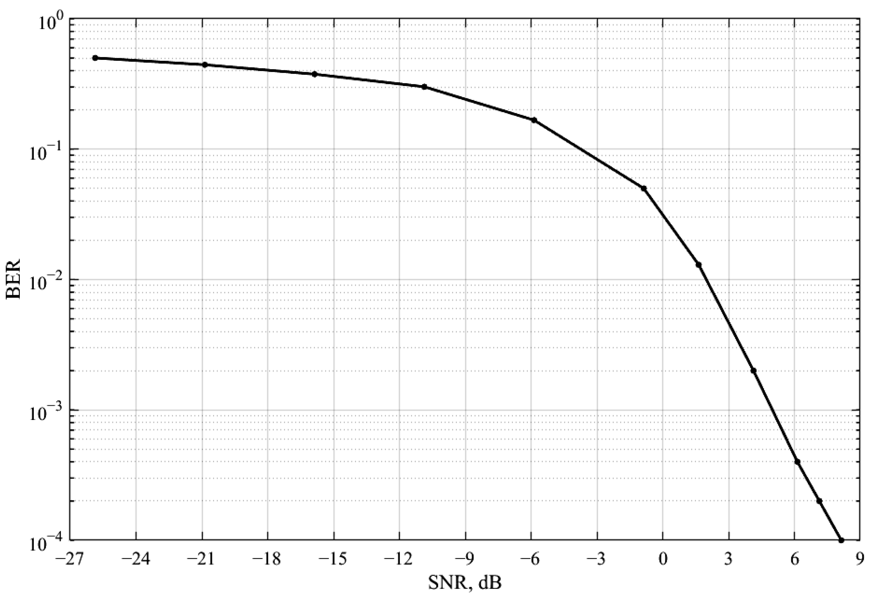
The proposed communication system performance was evaluated with white noise in the communication channel—the BER drops below 10−3 at SNR above 5 dB. The data rate achievable for a 50 MHz clock and 8196 samples per symbol is 6.1 kilobits per second, making the proposed system more suitable for applications that do not require high data speed but additional security.
Considering the limitations of the proposed approach, the present ACSK communication system has lower noise immunity than most conventional digital communication systems, since its performance highly depends on the quality of the chaotic synchronization achieved during demodulation, which is another trade-off to increase the security of the physical communication channel. The use of FPGA for modulation, demodulation, and signal processing makes the system flexible to make any changes and optimizations at any stage of system development without having to prototype a new hardware circuit on a printed circuit board. This study aims to demonstrate the proof of concept of a novel chaotic communication system implemented on FPGA. The implementation has been performed without inter-module optimization, so the prototype can be easily modified. The results of this study can be used in the next step of the ACSK communication system development, in which additional performance optimization and functionality improvements are intended.
The developed prototype of a chaotic communication system can be improved by supplementing the receiver with automated symbol phase synchronization and a data-packet protocol processing algorithm. The analog part of the prototype can be supplemented with radio modules that will provide wireless transmission of the chaotic signal via frequency modulation.


 ,
, 


