Article

Reliability Analysis and Fault-Tolerant Operation in a Multilevel Inverter for Industrial Application

1
Department of Electrical Engineering, ZHCET, Aligarh Muslim University, Aligarh 202002, India
2
Industrial Engineering Department, King Saud University, P.O. Box 800, Riyadh 11421, Saudi Arabia
3
Department of Marine Engineering Technology in a Joint Appointment with the Department of Electrical and Computer Engineering, Texas A&M University, Galveston, TX 77553, USA
*
Authors to whom correspondence should be addressed.
Electronics 2022, 11(1), 98; https://doi.org/10.3390/electronics11010098
Submission received: 23 October 2021 / Revised: 9 December 2021 / Accepted: 20 December 2021 / Published: 29 December 2021

Abstract

:
The extensive employment of power semiconductor devices in multilevel inverters (MLIs) has the consequence of increased failure probabilities. With numerous applications demanding highly reliable inverters, several fault-tolerant schemes have been devised to address switch open-circuit faults. This paper analyzes a multilevel inverter topology for IGBT modules undergoing open-circuit faults, a major impediment to reliable operation within a power converter. Reconfiguration of modulation is performed post-fault. A modulation scheme is implemented across failure modes as a hybrid of nearest level control and selective harmonic elimination. Reliability assessment of the topology is performed, including a comparison with previous literature in terms of component requirements and reliability. Simulation results validate the proposed solutions.

1. Introduction

The changing global paradigm about the electrical power sector with large scale renewable generation [1], high-voltage DC (HVDC) transmission systems, rapid electrification in automobiles [2], onboard power systems for aviation and marine applications [3,4], and introduction of the smart grid vision has enlarged the role of power electronic converters more than ever. The dc–ac conversion has extensive applications with MLIs (multilevel inverters) being the primary asset. The superiority of MLIs is vindicated by their excellent harmonic profile, lower switching losses and heat generation, and higher efficiency, a requirement of lower size filters with additional benefits of fault tolerance over the earlier established two-level inverters [5,6,7].
Nevertheless, an increased number of power semiconductors and circuit components like dc sources and capacitors cumulatively increase the probability of fault occurrence thus creating reliability issues [8,9]. Many applications in harsh environments and long operation hours demand highly reliable converters, e.g., power networks in rural areas, critical medical equipment power supplies, aircraft, and naval power systems from a safety viewpoint, satellite systems with unfeasible maintenance, or a wind farm or solar farm with extensive and widely distributed parts [10,11,12,13]. In field systems, it is observed that the power electronic converters are generally the least reliable assemblies and create significant maintenance costs [14]. Demonstrably, a survey concludes that inverters are the source for 37% of unexpected maintenance and 59% of maintenance costs during the 5-year life cycle of a 3.5 MW PV system. This validates that reliability performance must be addressed in the design phase with the traditional efficiency and power density issues.
To address these drawbacks, several topologies have been proposed with either the goal of reducing switch count hence decreasing fault probability or incorporating fault tolerance in the topology. The topology proposed in [15] demonstrates only partial fault-tolerance capabilities with reconfiguration possible for a fault on particular selected switches. Moreover, the topology uses more components while producing lesser voltage levels than the proposed topology. The combination of Cascaded H-Bridge (CHB) and neutral point clamped (NPC) for a fault-tolerant MLI is observed in [15] with complete fault tolerance on every switch, but with the added requirements of relays and transformers for post-fault operation. Extensive use of redundancy is carried out in [16] for fault tolerance of the topology. This, however, leads to an unusually large device count as well as capacitor voltage balancing issues after the fault. Likewise, the proposed topology uses redundant states in [17] for fault management. This, however, leads to twice the number of components as well as a rise in cost and reduced efficiency of the overall circuit. Topologies proposed in [18,19] circumvent the faulty cells by applying reconfiguration control mechanisms. The limitation is the unutilized dc sources belonging to the faulty cells. The MLI topology proposed in [20] is unable to tolerate fault on a bidirectional switch present between load and capacitor. The modified neutral point clamped (NPC) MLI topology proposed in [21,22,23] exhibits fault tolerance while adding the fourth leg of FC (flying capacitor) topology for redundancy. This solution does not provide fault tolerance to switches present in the inner leg, hence only is partial fault-tolerant. Additionally, the component count is significantly increased. Relays are employed to make the classical CHB topology fault-tolerant in [24,25]. However, many DC sources and conducting switches used during both pre-fault and post-fault operations have a negative impact on their reliability.
The topologies mentioned above show various drawbacks like high-power electronic device or capacitor count, capacitor voltage balancing issues, or partial fault tolerance. This paper investigates the fault-tolerant operation of a reduced device counts asymmetrical multilevel inverter topology. The topology [26] investigated in this paper exhibits fault tolerance with a lack of redundant unutilized switches or capacitors as well as the development of an open-circuit fault and mitigation method, which are verified through simulation results. Reliability analysis of the topology and a comparative analysis of the performance of the topology is also presented to demonstrate the feasibility of the fault-tolerance mechanism.

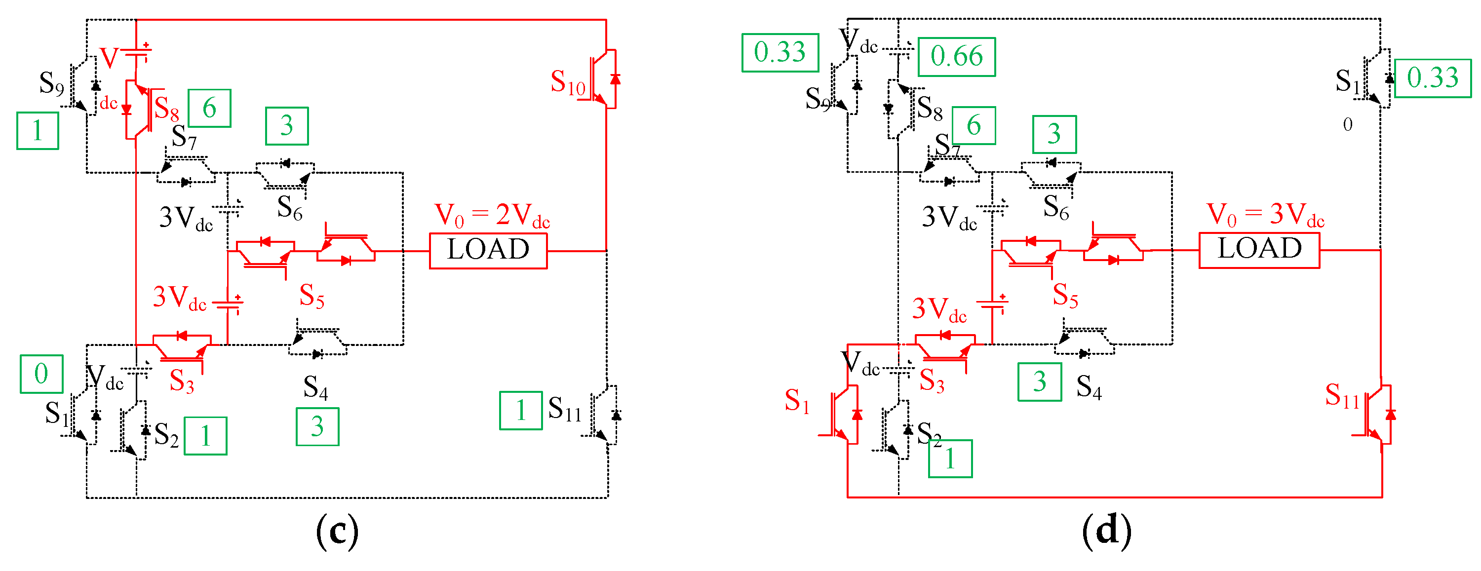
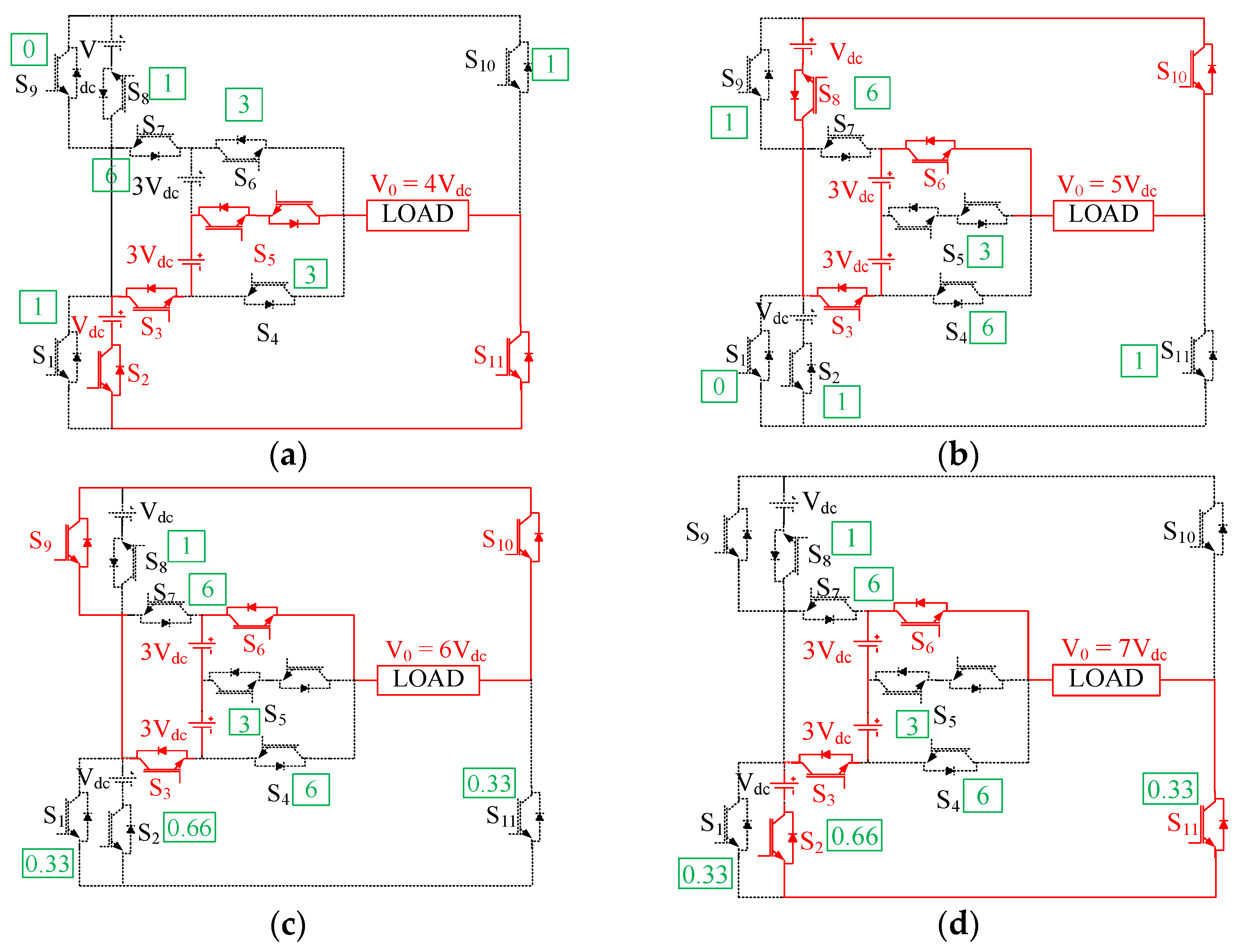
2. Analysis of the Topology

The schematic structure of the topology is illustrated in Figure 1. The components used comprise 10 unidirectional switches (bidirectional current flow and unidirectional blocking of voltage) and 1 bidirectional switch (consisting of two switches in common emitter configuration) with two pairs of dc voltage sources each of Vdc and 3 Vdc. Healthy topology operation produces 15 levels 0 to ± 7 Vdc of output load voltage. Diodes D1, D2, D3, D4, D5, and D6 are present to tackle the flyback effect at the instant of fault occurrence. The switching states with all the redundancies are displayed in Table 1.

3. Fault-Tolerance Approach

Contrary to topologies developed in [15], the investigated topology does not employ any external relays or redundant switches for fault resilience. The outcome is decreased efficiency and increased cost as the redundant components stand unutilized during healthy operation. Comparatively, all switches of the proposed topology are utilized pre-fault resulting in 100% utilization. A fault is tolerated on all switches leading to complete fault tolerance. The following section deals with fault conditions and fault mitigation.

3.1. Fault Conditions

Open-circuit faults on switches cause unavailability of particular voltage levels. The conditions arising from switch failures are listed in Table 2. Unattended faults lead to poor harmonic profiles but also a dc offset which is unacceptable for any load. For eliminating the dc offset the post-fault output voltage must be symmetric.

3.2. Fault Correction

Post occurrence of a fault, the waveform distortion is minimized using reconfiguration of the modulation strategy. Unequal voltage levels remain post-fault as in a fault in S4/S6 or S5.
The switching angles obtained after Selective Harmonic Elemination (SHE) are rounded off to the nearest angle for compatibility with Nearest Level Modulation-Pulse Width Modulation (NLM-PWM) scheme. The modulation thus implemented is a combination of Nearest Level Modulation (NLM) and SHE methods.

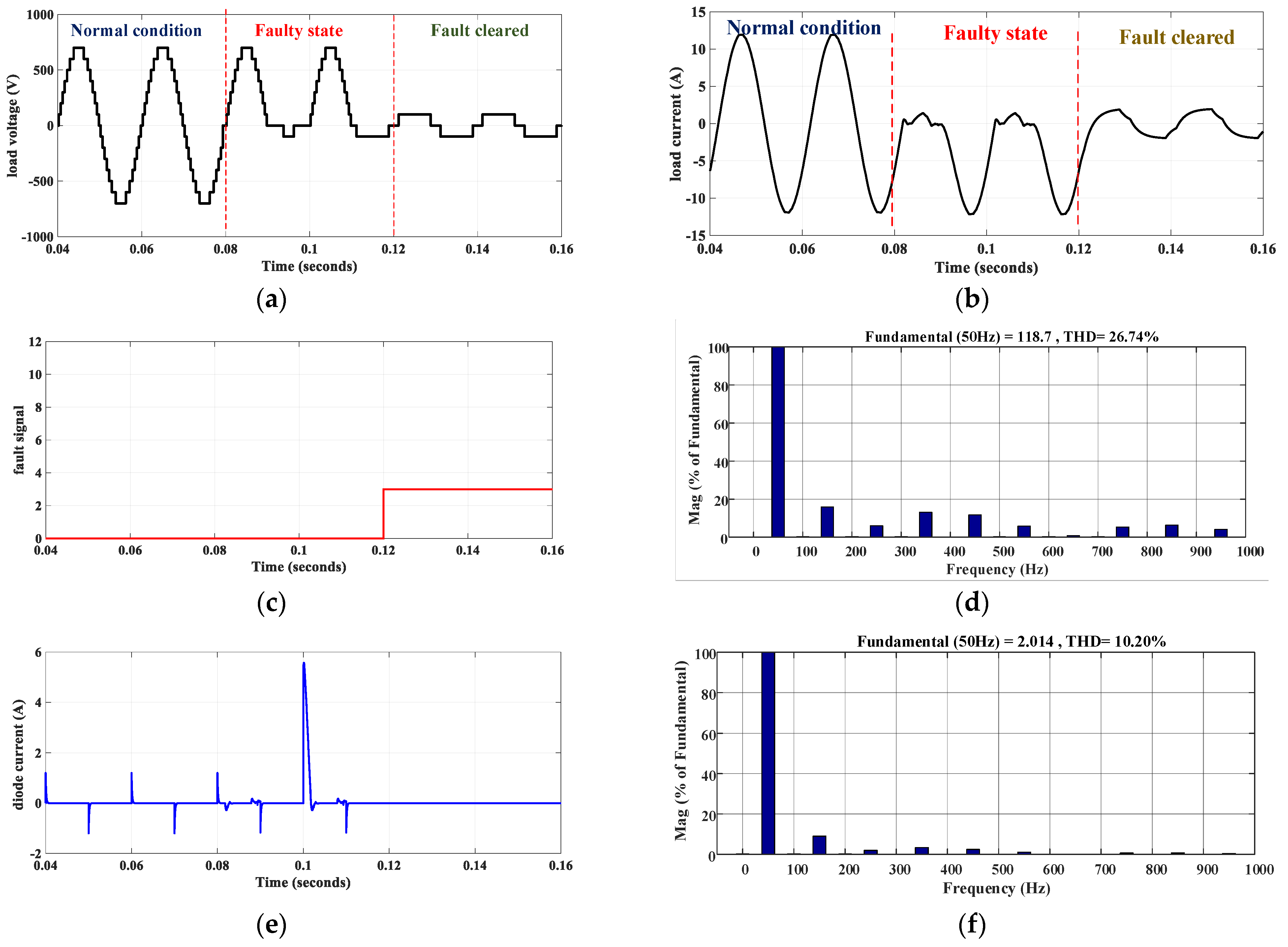
4. Simulation Results

The performance of the proposed topology was verified in MATLAB-Simulink™ R2016b and PLECS™ version 4.0.8 environment using Intel® Core™ i5-3210M 2.50 GHz simulation. The associated parameters are listed in Table 3. The modulation scheme executed was nearest level control (NLC) PWM for load voltage control. The NLC causes switching transitions at a low switching frequency, thus minimizing the switching losses and enhancing the inverter reliability. Model parameters are listed in Table 3. The results under healthy operation and faulty conditions are presented.

4.1. Healthy Operation

Following the simulation, the output voltage produced exhibits 15 levels with each level of 100 V and a peak of 700 V. Figure 2 and Figure 3 depict the conduction diagram for various states in positive half cycle of operation.The harmonic profile of the waveform conforms to the IEEE 519-2014 standard of generating a total harmonic distortion (THD) below 5% [27]. Figure 4 depicts the resultant output waveforms.

4.2. Fault-Tolerance
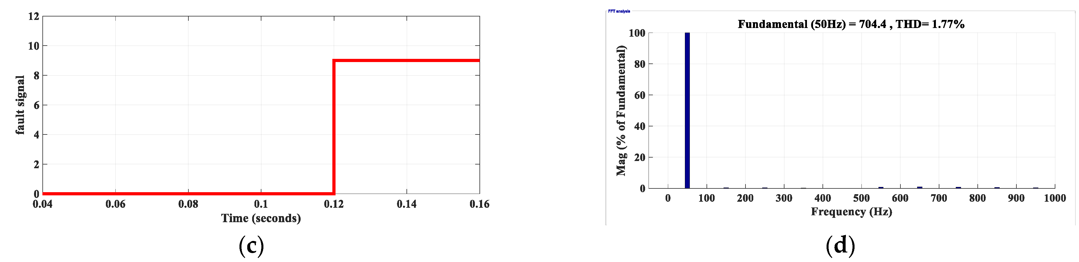
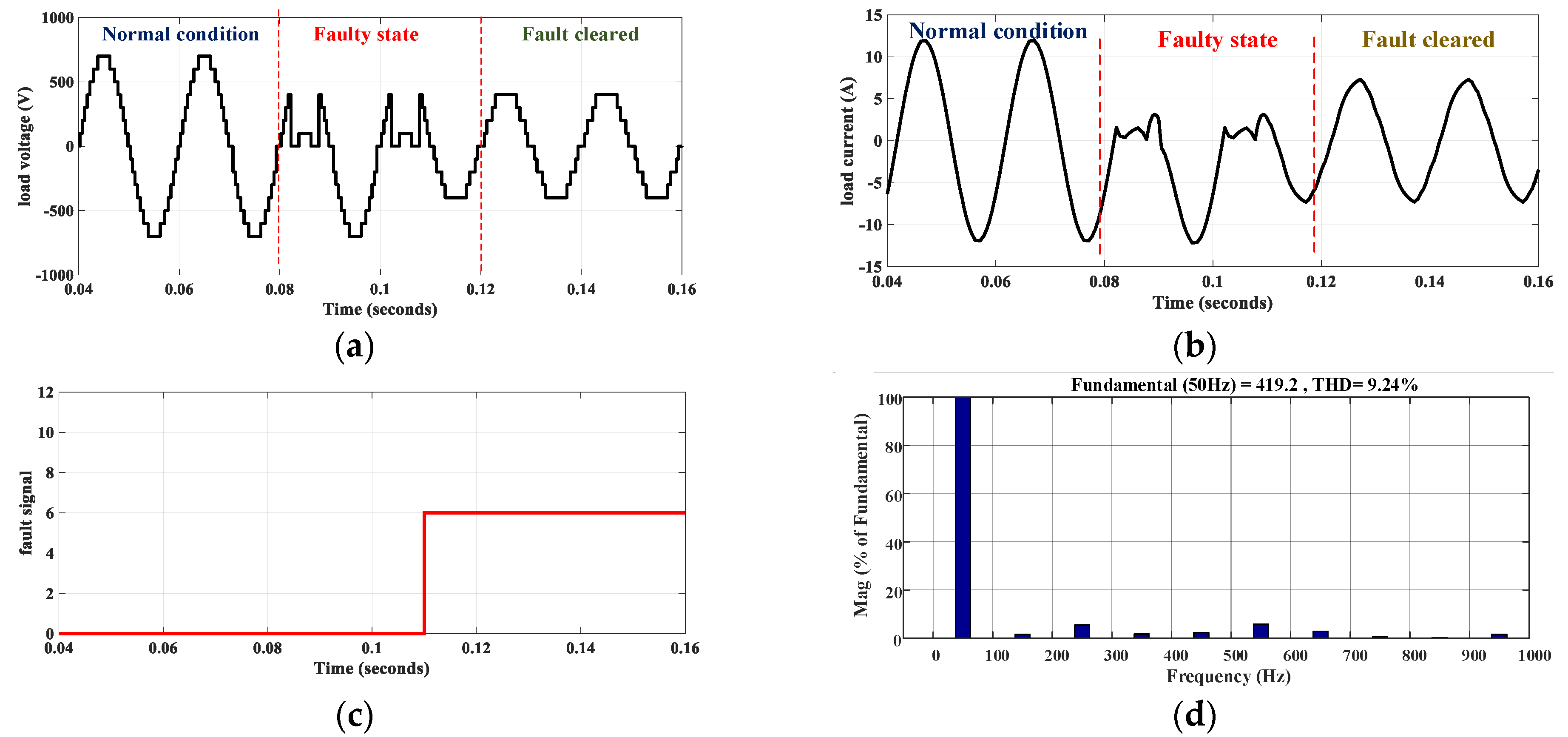
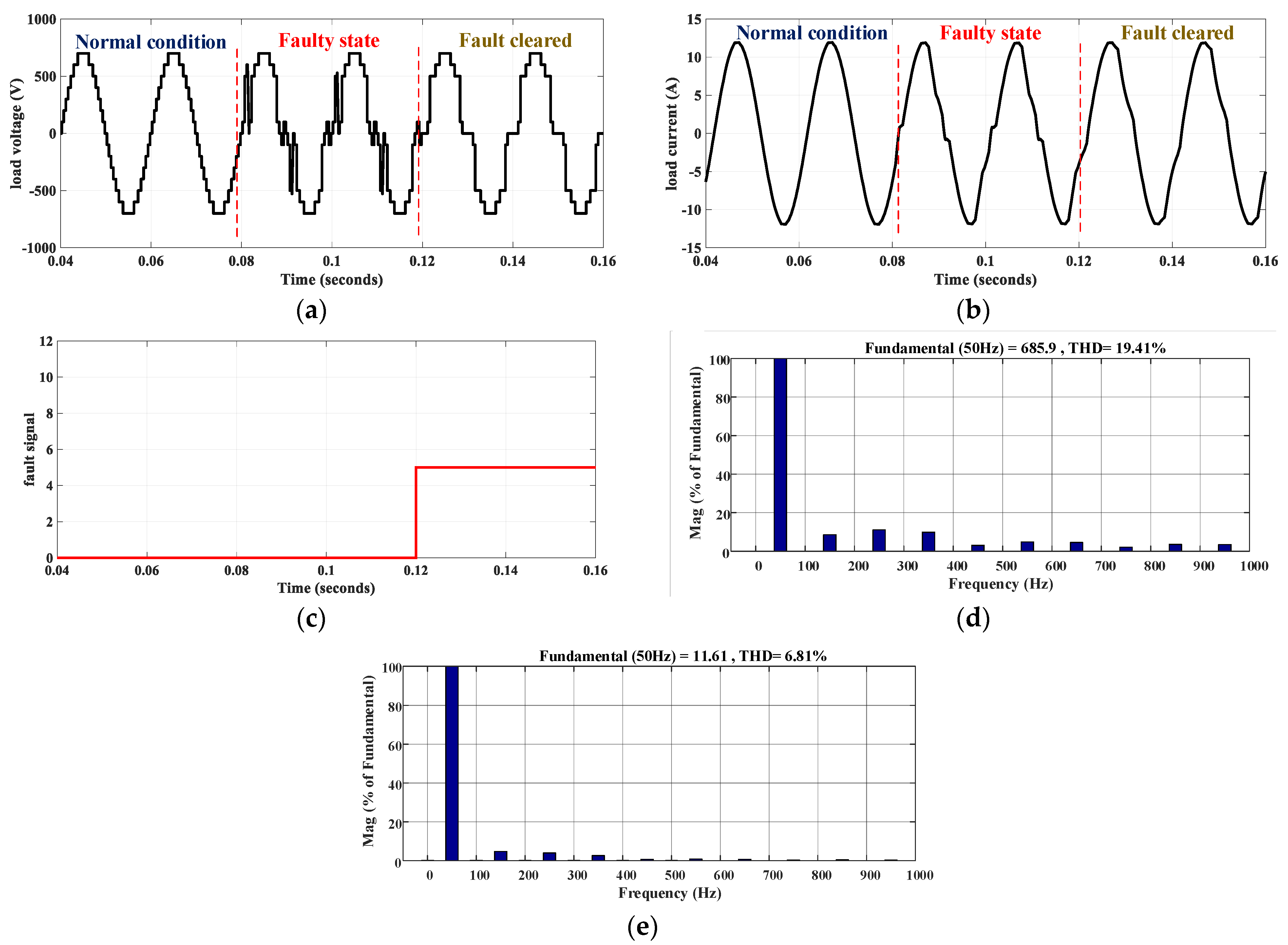
Three situations can ensue from an open-circuit malfunction on an individual switch. However, due to inbuilt fault-tolerant operation, reduced voltage levels and diminished output power continue to be supplied at the load terminals.
The first situation involves preserving every voltage level and consequently the output power rating post-detection and mitigation of fault. This is observed in the case of S1 or S9 fault, where redundant states are employed through modulation reconfiguration following fault detection. As for the second situation, in cases of open-circuited S2, S3, S4, S6, S7, S8, S10, or S11, the peak level 7 Vdc is lost additionally, which expedites to decrement in output power rating as well. In case of a fault in S5, level 7 Vdc is not lost, thus the output power rating is conserved.

4.3. S9 or S1 Fault

Following an open-circuit fault situation in S9 or S1, the loss of levels ±3 Vdc and ±6 Vdc is mitigated by reconfiguring using redundant states, leading to all seven levels being produced post-fault and the load voltage being unaffected. Figure 5 illustrates the waveforms concerned with the S9 fault which can also represent S1 fault conditions.

4.4. S2, S8, S10, and S11 Fault

When an open-circuit fault occurs in S2 or S8, the levels ±Vdc, ±2 Vdc, ±4 Vdc, ±5 Vdc, and ±7 Vdc are lost, and levels ±3 Vdc and ±6 Vdc can only be regenerated through reconfiguration. Furthermore, for obtaining the ideal switching angles, SHE is executed with the resulting angles being rounded off to the nearest NLC values for a better harmonic profile. The resulting waveforms are illustrated in Figure 6.

4.5. S3 or S7 Fault

Open-circuit failure on S3 or S7 leads to loss of all levels except ± Vdc levels. SHE is implemented for the reduction of harmonics post-fault. Minimum power is obtained post-fault in this scenario with the THD being the highest among other cases. Although the reduced power is still more useful for a critical load than no power at all. Figure 7 shows the results.

4.6. S4 or S6 Fault

Open-circuit failure in S4 or S6 leads to loss of levels ±5 Vdc, ±6 Vdc, ±7 Vdc with levels ±Vdc, ±2 Vdc, ±3 Vdc, ±4 Vdc prevailing through modulation reconfiguration. The execution of SHE is done post-fault for refining the harmonic profile. The resulting waveforms are displayed in Figure 8 and Figure 9.

4.7. S5 Fault

An open-circuit fault in S5 leads to loss of levels ±2 Vdc, Vdc, Vdc with levels ±Vdc, ±5 Vdc, ±6 Vdc, ±7 Vdc being generated by the application of modulation reconfiguration. The dc component remains zero during fault; therefore, the root mean square (RMS) value of load voltage is also required for fault detection. SHE is applied for obtaining the optimum waveform to minimize the lower-order harmonics. The resulting waveforms are discussed in Figure 10.

5. Reliability Analysis

Semiconductor devices are majorly prone to faults in an MLI. Nonetheless, the inherent fault-tolerant capabilities of the MLI amplify its reliability due to the provision of continued operation after the fault.

5.1. Component Failure Rate Evaluation

The failure rate of the various components depends on multiple factors derived from MIL-HDBK-217F [28], like voltage rating, application, thermal characteristics, etc. The failure rate of a semiconductor switch is derived as:
λ s = λ b   ×   π T   ×   π A   ×   π R   ×   π S   ×   π Q   ×   π E
where λb is the base failure rate being equal to 0.00074.
π T is the junction temperature factor and π R is the power rating factor and are both dependent on switch power loss values. The application factor π A corresponds to switching. The quality factor is taken for JANTX quality, and the analysis is done for a benign ground environment.

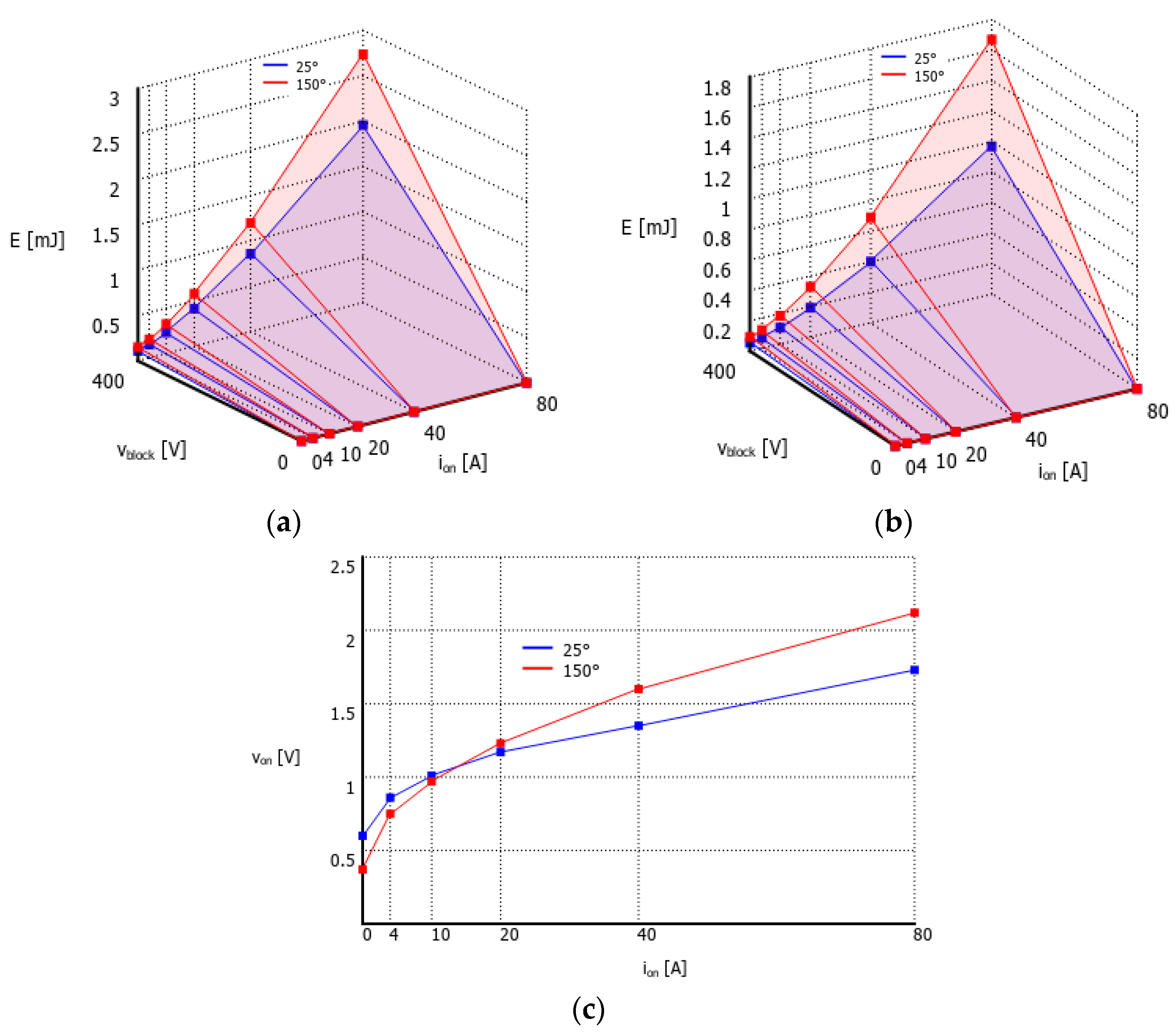
5.2. Power Loss Analysis

Switching losses and conduction losses are the two parts of the device losses. Conduction losses in an IGBT can be evaluated using (2) and a diode using (3). The fundamental period observes a total conduction loss of magnitude equal to (4). The various constants are determined by the datasheet of the device.
P   c s w = V s w i ( t ) + R s i β ( t ) ,
P   c D = V D i ( t ) + R D i 2 ( t ) ,
P c   = k = 1 N s w 1 2 π 0 2 π ( V s w i ( t ) + R s i β ( t ) ) d t + k = 1 N D 1 2 π 0 2 π ( V D i ( t ) + R D i 2 ( t ) ) d t .
Above, Vsw represents the voltage drop across the switch when it is ON and VD represents voltage drop across a diode. Non-ideal switching transitions give rise to switching losses in the circuit. With a linear assumption of current and voltage variation during switching, we arrive at the following relation for switching loss
P s   = [ k = 1 N s (   N O N k E O N k + N O F F k E O F F k )   ] × f ,
The number of switching transitions to ON and OFF states of the switches respectively is stood for by N O N k and N O F F k with E O N k and E O F F k   correspondingly equal to the associated energy losses for the kth device, f is the fundamental frequency. The sum total loss is:
P loss   = P c + P s
With the power loss of every device known beforehand, the steady-state junction temperature of every switch can be determined. Thermal modeling analysis was implemented in PLECS software with the load as 50 + 50j Ω. IGBT with diode IKW40N65ES5 data was used for thermal modeling. The thermal description of the joule losses for the IGBT and Diode is given in Figure 11 and Figure 12. Respectively. The calculated values of πR, πT, and πS are given in Table 4.

5.3. Derivation of the Reliability Function

The reliability function for a device, according to [28] is defined as
R ( t ) = 1 0 1 f ( t ) d t = 1 0 1 ( λ e λ t ) d t = 1 e λ t ,
f ( t ) = λ e λ t  
where f ( t )   is the probability of failure of a device in a given period. The reliability function of the topology is derived using Equations (7) and (8) and is represented by Equation (9). The first term of the equation reflects the healthy mode of operation with the succeeding terms added for various cases of fault tolerance through modulation reconfiguration for fault in any one switch.
R ( t ) = ( e λ 1 t ) 2 ( e λ 2 t ) 2 ( e λ 3 t ) 2 ( e λ 4 t ) 2 ( e λ 5 t ) 2 ( e λ 10 t ) 2 + 2 ( 1 e λ 1 t ) ( e λ 2 t ) 2 ( e λ 3 t ) 2 ( e λ 4 t ) 2 ( e λ 5 t ) 2 ( e λ 10 t ) 2 + 2 ( e λ 2 t )   ( e λ 1 t ) 2 ( e λ 3 t ) 2 ( e λ 4 t ) 2 ( e λ 5 t ) 2 ( e λ 10 t ) 2 + 2 ( 1 e λ 3 t )   ( e λ 1 t ) 2 ( e λ 2 t ) 2 ( e λ 4 t ) 2 ( e λ 5 t ) 2 ( e λ 10 t ) 2 + 2 ( 1 e λ 4 t )   ( e λ 1 t ) 2 ( e λ 2 t ) 2 ( e λ 3 t ) 2 ( e λ 5 t ) 2 ( e λ 10 t ) 2 + 2 ( 1 e λ 5 t ) ( e λ 1 t ) 2 ( e λ 3 t ) 2 ( e λ 4 t ) 2 ( e λ 2 t ) 2 + 2 ( 1 e λ 10 t ) ( e λ 1 t ) 2 ( e λ 3 t ) 2 ( e λ 4 t ) 2 ( e λ 2 t ) 2 ( e λ 5 t ) 2
The fault in S1/S9 is represented by the second term. The equation’s third term reflects fault in S2/S8. The fourth term of the above equation reflects fault in S3/S7. Similarly, sixth seventh, and eighth terms represent a fault in S4/S6, S5, and S10/S11 respectively. The reliability curve and its comparison with previous topologies are depicted in Figure 13 for 20 years. It is recognizable that the proposed topology has higher reliability than topologies introduced in [15,16,20,24,25,29].

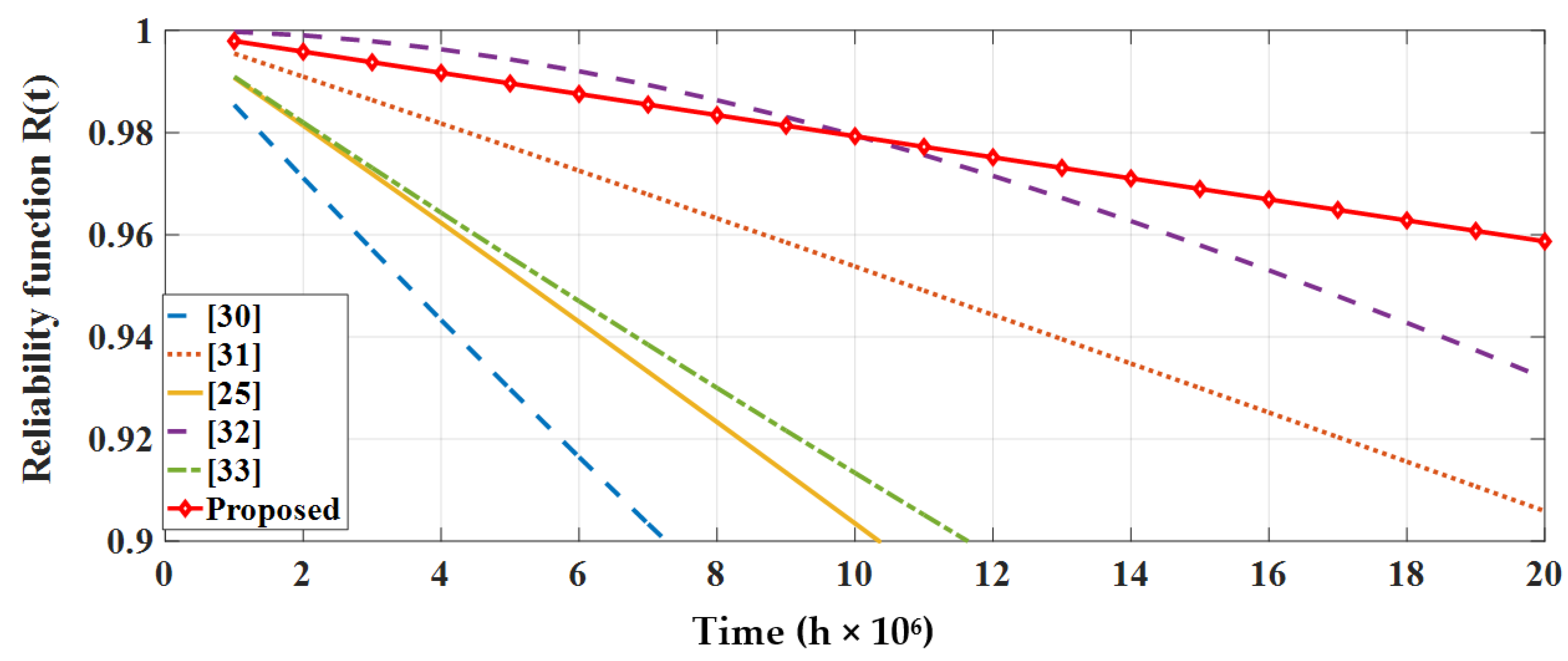
5.4. Reliability Comparison with Recent Literature

The reliability equation of the topology is compared with some recent works as exhibited below. The proposed topology in [30] has the following reliability function:
R ( t ) = ( e λ b t ) 5 ( e λ d t ) 4 + 5 ( 1 e λ b t ) ( e λ b t ) 3 ( e λ d t ) 4   + 4 ( 1 e λ b t ) ( e λ b t ) 5 ( e λ d t ) 3
The topology in [31] has the following reliability function:
R ( t ) = ( e λ b t ) 5 ( e λ d t ) 3 + 3 ( 1 e λ b t ) ( e λ b t ) 4 ( e λ d t ) 3 2 ( 1 e λ d t ) ( e λ b t ) 5 ( e λ d t ) 2
The topology in [25] possesses the following reliability function:
R ( t ) = ( e λ c t ) 12 ( e λ d t ) 4 + 12 ( 1 e λ c t ) ( e λ c t ) 6 ( e λ d t ) 6
The reliability function of topology introduced in [32] is given as:
R ( t ) = ( e λ b t ) 2 ( e λ c t ) 4 ( e λ d t ) 8 + 8 ( 1 e λ d t ) ( e λ b t ) 2 ( e λ c t ) 4 ( e λ d t ) 8 + 2 ( 1 e λ b t ) ( e λ c t ) 4 ( e λ d t ) 8 + 4 ( 1 e λ c t ) ( e λ b t ) 2 ( e λ c t ) 2
The topology mentioned in [33] has the reliability function:
R ( t ) = ( e λ b t ) 5 ( e λ d t ) 3 + 3 ( 1 e λ b t ) ( e λ b t ) 4 ( e λ d t ) 2  
where in the preceding equations, λ b = 0.0011 ,   λ c = 0.0016 ,   λ d = 0.002 .

6. Comparative Analysis

The performance parameters of the topologies such as NPC, CHB, and FC topologies as well as topologies proposed in [15,16,20,24,25,29] are demonstrated in Table 4. Compared with the number of levels generated, the proposed topology requires a significantly competitive amount of dc sources. The requirement of any capacitors, transformers, or relays is also absent in the proposed topology. Moreover, the ratio of levels generated/IGBTs required is substantially higher than other topologies except [15], but [15] also requires relays and a center-tapped transformer for fault-tolerant operation. Furthermore, no redundant switch is required, which implies no switch remains unutilized during healthy operation implying full utilization of all switches.

7. Conclusions

This paper assesses a reduced device count 15-level asymmetrical multilevel inverter topology for fault-tolerant capabilities. Redundant states are employed to mitigate post-fault output distortion. The topology’s operational performance, including load power and output harmonic distortion, are examined under various failure modes through simulation results to demonstrate the fault-tolerant operation. Reliability function derivation and thermal analysis are performed and reliability curve and failure rate values are established according to predefined standards to indicate the improvement in reliability with fault-tolerance capability. A comparison with previously established fault-tolerance works has been presented to evaluate the performance of the topology for reliability-critical applications.

Author Contributions

Conceptualization, M.F. and A.S.; formal analysis, M.F., A.S. and M.T.; funding acquisition, M.A. and S.A.; investigation, M.F., M.A., S.A., A.S., M.T. and I.A.K.; methodology, M.F., A.S. and M.T.; supervision, A.S. and M.T.; writing—original draft, M.F. and A.S.; writing—review and editing, M.A., S.A., M.T. and I.A.K. All authors have read and agreed to the published version of the manuscript.

Funding

The authors extend their appreciation to King Saud University for funding this work through Researchers Supporting Project number (RSP-2021/313), King Saud University, Riyadh, Saudi Arabia.

Acknowledgments

The authors acknowledge King Saud University for funding this work through Researchers Supporting Project number (RSP-2021/313), King Saud University, Riyadh, Saudi Arabia.

Conflicts of Interest

The authors declare no conflict of interest.

References

  1. Yilmaz, S.; Dincer, F. Impact of Inverter Capacity on the Performance in Large-Scale Photovoltaic Power Plants—A Case Study for Gainesville, Florida. Renew. Sustain. Energy Rev. 2017, 79, 15–23. [Google Scholar] [CrossRef]
  2. Stippich, A. Key Components of Modular Propulsion Systems for Next Generation Electric Vehicles. CPSS Trans. Power Electron. Appl. 2017, 2, 249–258. [Google Scholar] [CrossRef]
  3. Pei, X.; Li, H. Master-Slave Cascade Multilevel Inverter for Motor Drive Control of Electric Vehicles. In Proceedings of the 45th Annual Conference of the IEEE Industrial Electronics Society (IECON 2019), Lisbon, Portugal, 14–17 October 2019; pp. 3210–3214. [Google Scholar] [CrossRef]
  4. Guo, F.; Yang, T.; Diab, A.M.; Yeoh, S.S.; Bozhko, S.; Wheeler, P. An Enhanced Virtual Space Vector Modulation Scheme of Three-Level NPC Converters for More-Electric-Aircraft Applications. IEEE Trans. Ind. Appl. 2021, 57, 5239–5251. [Google Scholar] [CrossRef]
  5. Akagi, H. Multilevel Converters: Fundamental Circuits and Systems. Proc. IEEE 2017, 105, 2048–2065. [Google Scholar] [CrossRef]
  6. Poorfakhraei, A.; Narimani, M.; Emadi, A. A Review of Multilevel Inverter Topologies in Electric Vehicles: Current Status and Future Trends. IEEE Open J. Power Electron. 2021, 2, 155–170. [Google Scholar] [CrossRef]
  7. Omer, P.; Kumar, J.; Surjan, B.S. A Review on Reduced Switch Count Multilevel Inverter Topologies. IEEE Access 2020, 8, 22281–22302. [Google Scholar] [CrossRef]
  8. Kumar, D.; Nema, R.K.; Gupta, S. Investigation of Fault-Tolerant Capabilities of Some Recent Multilevel Inverter Topologies. Int. J. Electron. 2021, 108, 1957–1976. [Google Scholar] [CrossRef]
  9. Mirafzal, B. Survey of Fault-Tolerance Techniques for Three-Phase Voltage Source inverters. IEEE Trans. Ind. Electron. 2014, 61, 5192–5202. [Google Scholar] [CrossRef]
  10. Zhang, J.; Sun, H.; Sun, Z.; Dong, W.; Dong, Y. Fault Diagnosis of Wind Turbine Power Converter Considering Wavelet Transform, Feature Analysis, Judgment and BP Neural Network. IEEE Access 2019, 7, 179799–179809. [Google Scholar] [CrossRef]
  11. Formica, T.J.; Khan, H.A.; Pecht, M.G. The Effect of Inverter Failures on the Return on Investment of Solar Photovoltaic Systems. IEEE Access 2017, 5, 21336–21343. [Google Scholar] [CrossRef]
  12. Tariq, M.; Maswood, A.I.; Moreddy, A.C.; Gajanayake, C.J.; Lee, M.Y.; Gupta, A.K. Reliability, Dead-Time, and Feasibility Analysis of a Novel Modular Tankless ZCS Inverter for More Electric Aircraft. IEEE Trans. Transp. Electrif. 2017, 3, 843–854. [Google Scholar] [CrossRef]
  13. Ni, K.; Hu, Y.; Wang, Z.; Wen, H.; Gan, C. Asynchronized Synchronous Motor-Based More Electric Ship-Less Power Electronics for More System Reliability. IEEE/ASME Trans. Mechatron. 2019, 24, 2353–2364. [Google Scholar] [CrossRef]
  14. Blaabjerg, F.; Wang, H.; Vernica, I.; Liu, B.; Davari, P. Reliability of Power Electronic Systems for EV/HEV Applications. Proc. IEEE 2021, 109, 1060–1076. [Google Scholar] [CrossRef]
  15. Gautam, S.P.; Kumar, L.; Gupta, S.; Agrawal, N. A Single-Phase Five-Level Inverter Topology with Switch Fault-Tolerance Capabilities. IEEE Trans. Ind. Electron. 2017, 64, 2004–2014. [Google Scholar] [CrossRef]
  16. Chen, A.; Hu, L.; Chen, L.; Deng, Y.; He, X. A Multilevel Converter Topology with Fault-Tolerant Ability. IEEE Trans. Power Electron. 2005, 20, 405–415. [Google Scholar] [CrossRef]
  17. Lezana, P.; Aguilera, R.; Rodríguez, J. Fault Detection on Multicell Converter Based on Output Voltage Frequency Analysis. IEEE Trans. Ind. Electron. 2009, 56, 2275–2283. [Google Scholar] [CrossRef] [Green Version]
  18. Song, W.; Huang, A.Q. Fault-Tolerant Design and Control Strategy for Cascaded H-bridge Multilevel Converter-Based STATCOM. IEEE Trans. Ind. Electron. 2010, 57, 2700–2708. [Google Scholar] [CrossRef]
  19. Yazdani, A.; Sepahvand, H.; Crow, M.L.; Ferdowsi, M. Fault Detection and Mitigation in Multilevel Converter STATCOMs. IEEE Trans. Ind. Electron. 2011, 58, 1307–1315. [Google Scholar] [CrossRef]
  20. Jalhotra, M.; Kumar, L.; Gautam, S.P.; Gupta, S. Development of Fault-Tolerant MLI Topology. IET Power Electron. 2018, 11, 1416–1424. [Google Scholar] [CrossRef]
  21. Ceballos, S.; Pou, J.; Zaragoza, J.; Robles, E.; Villate, J.L.; Martín, J.L. Fault-Tolerant Neutral-Point-Clamped Converter Solutions Based on Including a Fourth Resonant Leg. IEEE Trans. Ind. Electron. 2011, 58, 2293–2303. [Google Scholar] [CrossRef]
  22. Ceballos, S.; Pou, J.; Robles, E.; Gabiola, I.; Zaragoza, J.; Villate, J.L.; Boroyevich, D. Three-Level Converter Topologies with Switch Breakdown Fault-Tolerance Capability. IEEE Trans. Ind. Electron. 2008, 55, 982–995. [Google Scholar] [CrossRef]
  23. Ceballos, S.; Pou, J.; Robles, E.; Zaragoza, J.; Martin, J.L. Performance Evaluation of Fault-Tolerant Neutral-Point-Clamped Converters. IEEE Trans. Ind. Electron. 2010, 57, 2709–2718. [Google Scholar] [CrossRef]
  24. Haji-Esmaeili, M.M.; Naseri, M.; Khoun-Jahan, H.; Abapour, M. Fault-Tolerant Structure for Cascaded H-Bridge Multilevel Inverter and Reliability Evaluation. IET Power Electron. 2017, 10, 59–70. [Google Scholar] [CrossRef]
  25. Jahan, H.K.; Panahandeh, F.; Abapour, M.; Tohidi, S. Reconfigurable Multilevel Inverter with Fault Tolerant Ability. IEEE Trans. Power Electron. 2017, 33, 7880–7893. [Google Scholar] [CrossRef]
  26. Fahad, M.; Siddique, M.D.; Iqbal, A.; Sarwar, A.; Mekhilef, S. Implementation and Analysis of a 15-Level Inverter Topology with Reduced Switch Count. IEEE Access 2021, 9, 40623–40634. [Google Scholar] [CrossRef]
  27. IEEE Standards Association. 519-2014-IEEE Recommended Practices and Requirements for Harmonic Control in Electric Power Systems; IEEE: Piscataway, HJ, USA, 2014. [Google Scholar] [CrossRef]
  28. Equipment, E. Reliability Prediction of Electronic Equipment; Department of Defense: Washington, DC, USA, 1991. [Google Scholar]
  29. Dewangan, N.K.; Gupta, K.K.; Bhatnagar, P. Modified Reduced Device Multilevel Inverter Structures with Open Circuit Fault-Tolerance Capabilities. Int. Trans. Electr. Energy Syst. 2020, 30, e12142. [Google Scholar] [CrossRef]
  30. Chappa, A.; Gupta, S.; Sahu, L.K.; Gupta, K.K. Resilient Multilevel Inverter Topology with Improved Reliability. IET Power Electron. 2020, 13, 3384–3395. [Google Scholar] [CrossRef]
  31. Sivakumar, K. A Fault-Tolerant Single-Phase Five-Level Inverter for Grid-Independent PV Systems. IEEE Trans. Ind. Electron. 2015, 62, 7569–7577. [Google Scholar] [CrossRef]
  32. Ambusaidi, K.; Pickert, V.; Zahawi, B. New Circuit Topology for Fault Tolerant H-bridge Dc-Dc Converter. IEEE Trans. Power Electron. 2010, 25, 1509–1516. [Google Scholar] [CrossRef]
  33. Gautam, S.P.; Sahu, L.K.; Gupta, S. Reduction in Number of Devices for Symmetrical and Asymmetrical Multilevel Inverters. IET Power Electron. 2016, 9, 698–709. [Google Scholar] [CrossRef]
Figure 1. Structure of multilevel inverter topology.
Electronics 11 00098 g001
Figure 2. Positive conduction states (part 1). (a) State 0 (b) State 1 (c) State 2 (d) State 3.
Electronics 11 00098 g002aElectronics 11 00098 g002b
Figure 3. Positive conduction states (part 2). (a) State 4 (b) State 5 (c) State 6 (d) State 7.
Electronics 11 00098 g003
Figure 4. Simulation results of the proposed structure during healthy operation comprising (a) load voltage, (b) magnified view of load voltage, (c) load current, (d) magnified view of load current, (e) voltage harmonic characteristics acquired from Fourier analysis, and (f) current harmonic characteristics.
Electronics 11 00098 g004aElectronics 11 00098 g004b
Figure 5. Simulation results for S9 fault for (a) load voltage, (b) load current, (c) fault detection signal, and (d) voltage harmonics profile.
Electronics 11 00098 g005aElectronics 11 00098 g005b
Figure 6. Simulation results for S8 fault for (a) load voltage, (b) load current, (c) fault detection signal, (d) voltage harmonics profile, (e) diode current, and (f) current harmonics profile.
Electronics 11 00098 g006
Figure 7. Simulation results for S3 fault for (a) load voltage, (b) load current, (c) fault detection signal, (d) voltage harmonics profile, (e) diode current, and (f) current harmonics profile.
Electronics 11 00098 g007
Figure 8. Simulation results for S6 fault for (a) load voltage, (b) load current, (c) fault detection signal, and (d) voltage harmonics profile.
Electronics 11 00098 g008
Figure 9. Simulation results for S6 fault for (a) diode current and (b) current harmonic profile.
Electronics 11 00098 g009
Figure 10. Simulation results for S5 fault for (a) load voltage, (b) load current, (c) fault detection signal, (d) voltage harmonics profile, and (e) current harmonics profile.
Electronics 11 00098 g010
Figure 11. IGBT thermal description corresponding to (a) Turn ON losses, (b) Turn OFF losses, and (c) conduction losses.
Electronics 11 00098 g011
Figure 12. Diode thermal description corresponding to (a) Turn OFF losses and (b) conduction losses.
Electronics 11 00098 g012
Figure 13. Reliability comparison with previous literature.
Electronics 11 00098 g013
Table 1. Fault management for each switch.
S1S2S3S4S5S6S7S8S9S10S11Vout
10110000001Zero
0
0
1
1
1
0
1
0
0
0
0
1
0
1
0
0
0
0
0
0
1
1
Vdc
001010010102 Vdc
1
0
0
0
1
1
0
0
1
1
0
0
0
0
0
0
0
1
0
1
1
0
3 Vdc
011010000014 Vdc
001001010105 Vdc
001001001106 Vdc
1
0
0
1
1
1
0
0
0
0
1
1
0
0
0
0
0
0
0
0
1
1
7 Vdc
00000110110Zero
0
0
0
0
0
1
0
1
0
0
1
0
1
0
1
1
0
0
1
1
0
0
−Vdc
01001010001−2 Vdc
0
1
0
0
0
0
0
0
1
1
0
0
1
1
0
0
1
0
1
0
0
1
−3 Vdc
00001011010−4 Vdc
01010010001−5 Vdc
00010010110−6 Vdc
1
0
0
0
0
0
1
1
0
0
0
0
1
1
0
1
0
0
0
1
1
0
−7 Vdc
Table 2. Fault management for each switch.
Faulty SwitchVoltage Levels LostLevels Regained Post Reconfiguration
S1 or S9±3 Vdc, ±6 VdcAll
S2 or S8±Vdc, ±2 Vdc, ±4 Vdc, ±5 Vdc, ±7 Vdc±3 Vdc, ± 6Vdc
S3 or S7±2 Vdc to ±7 Vdc±Vdc
S4 or S6±5 Vdc, ±6 Vdc, ±7 Vdc±Vdc, ±2 Vdc, ±3 Vdc, ±4 Vdc
S5±2 Vdc, ± 3 Vdc, ±4 Vdc±Vdc, ±5 Vdc, ±6 Vdc, ±7 Vdc
S10 or S11±Vdc, ±2 Vdc, ±4 Vdc, ±5 Vdc, 7 Vdc±3 Vdc, ±6 Vdc
Table 3. Simulation parameters.
ParameterValue
Voltage sources100 V
300 V
Load impedance50 Ω, 100 mH
Modulating frequency50 Hz
Table 4. Comparative features.
FeaturesNPCFCCHB[15][16][20][24][25][29]Proposed
Number of DC voltage sources1142124434
Required number of capacitors02800720000
Number of Diodes required56002000006
Number of IGBTs required1616168221216201212
Number of gate drivers required16161672291620911
Number of Relays0002000000
Number of Transformers0001000000
Number of voltage levels generated99959999715
Fault-tolerant operationNONOYESYESYESYESYESYESYESYES
Redundant switches required--YESNOYESNOYESYESYESNO
Publisher’s Note: MDPI stays neutral with regard to jurisdictional claims in published maps and institutional affiliations.

