Article

Electro-Thermal Model-Based Design of Bidirectional On-Board Chargers in Hybrid and Full Electric Vehicles

by
Pierpaolo Dini
and
Sergio Saponara
*,†
Department of Information Engineering, University of Pisa, 56122 Pisa, Italy
*
Author to whom correspondence should be addressed.
These authors contributed equally to this work.
Electronics 2022, 11(1), 112; https://doi.org/10.3390/electronics11010112
Submission received: 4 November 2021 / Revised: 14 December 2021 / Accepted: 18 December 2021 / Published: 30 December 2021

Abstract

:
In this paper, a model-based approach for the design of a bidirectional onboard charger (OBC) device for modern hybrid and fully electrified vehicles is proposed. The main objective and contribution of our study is to incorporate in the same simulation environment both modelling of electrical and thermal behaviour of switching devices. This is because most (if not all) of the studies in the literature present analyses of thermal behaviour based on the use of FEM (Finite Element Method) SWs, which in fact require the definition of complicated models based on partial derivative equations. The simulation of such accurate models is computationally expensive and, therefore, cannot be incorporated into the same virtual environment in which the circuit equations are solved. This requires long waiting times and also means that electrical and thermal models do not interact with each other, limiting the completeness of the analysis in the design phase. As a case study, we take as reference the architecture of a modular bidirectional single-phase OBC, consisting of a Totem Pole-type AC/DC converter with Power Factor Correction (PFC) followed by a Dual Active Bridge (DAB) type DC/DC converter. Specifically, we consider a 7 kW OBC, for which its modules consist of switching devices made with modern 900 V GaN (Gallium Nitrade) and 1200 V SiC (Silicon Carbide) technologies, to achieve maximum performance and efficiency. We present a procedure for sizing and selecting electronic devices based on the analysis of behaviour through circuit models of the Totem Pole PFC and DAB converter in order to perform validation by using simulations that are as realistic as possible. The developed models are tested under various operating conditions of practical interest in order to validate the robustness of the implemented control algorithms under varying operating conditions. The validation of the models and control loops is also enhanced by an exhaustive robustness analysis of the parametric variations of the model with respect to the nominal case. All simulations obtained respect the operating limits of the selected devices and components, for which its characteristics are reported in data sheets both in terms of electrical and thermal behaviour.

1. Introduction

1.1. Motivations

The market for hybrid and electric vehicles has been growing strongly in recent years. The increasing market demand for highly efficient hybrid and electric vehicles is one of the modern challenges also in the field of scientific research. In particular, the development of increasingly efficient electronic power flow systems is one of the most important topics in recent years. The focus is on charging electric batteries in modern vehicles. In particular, we present the development of a highly detailed model of both the electrical and thermal behaviour of a bidirectional On-Board Charger with modular architecture. The development of accurate models for the simulation of onboard electronic systems is certainly an essential step in the design of increasingly advanced and efficient devices. Often the development of models involves a high degree of detail in only a few aspects, e.g., focusing only on voltage and current behaviour or concentrating only on thermal behaviour, or even only on the magnetic behaviour of components. Once a very accurate model has been developed for one of the above aspects, the typical approach is to start a campaign of experimental measurements to evaluate the aspects that were not exhaustively modelled before. This approach limits the analysis of critical cases as it is not possible to assess certain scenarios or operational combinations, which would otherwise require ’destructive’ testing. Using a model that is accurate in several respects does not have these limitations. Obviously, not all physical aspects can be modelled with the highest accuracy with common SW tools. Therefore, it is necessary to find a compromise in terms of model complexity that is nevertheless comprehensive in order to best assess a number of scenarios and operating conditions in a simple and fast manner. The contribution of our study is to incorporate both electrical and thermal behaviour in the same simulation environment by means of equivalent models to make computational complexity manageable. The problem of using simulation SW tools that are specific and optimised for one aspect only, such as SW for FEM (Finite Element Method) analysis, is that simulations are often very computationally intensive because they are based on complex and complicated mathematical models, requiring a lot of time for conducting the simulation itself. This requires modelling and simulating various aspects of the overall dynamic system separately. By using equivalent dynamic models, which nevertheless consider the most relevant physical aspects, it is possible to reduce the computational complexity considerably; thus, it is possible to simulate all aspects of interest in a single SW environment. This makes the overall model very comprehensive, making the simulations realistic so that the results can be used to evaluate, for example, the choice of passive components and thermal characteristics on a real physical system. In addition, the use of equivalent models incorporated in the same simulation environment makes the virtual system more flexible and scalable, providing freedom in monitoring, control, and modulation techniques without modifying the system. This is the reason why we propose an operational procedure for developing a simulation model that is able to incorporate two of the main aspects, the dynamics of the electrical quantities and the thermal behaviour of the switching components, by using the single-phase bidirectional on-board charger architecture as a use case.

1.2. State of the Art on OBC Modelling, Simulation and Control

In Ref. [1], the authors present a modelling and design study of unidirectional OBC consisting of an AC-DC diode rectifier stage, followed by a step-up type of DC-DC converter to achieve PFC connected to the vehicle battery via a second Phase-Shifted-Full-Bridge (PSFB) type DC-DC converter. The paper presents the essential modelling of the electrical circuit necessary to define transfer functions required by the control algorithm. Compared to that article, the study proposed here includes an analysis of a bidirectional model, including the complication of the control algorithm of a Totem Pole circuit and of a DAB circuit, as well as an analysis of the thermal behaviour of the switching devices, which is completely absent in the mentioned study. The authors of [2], instead, present an alternative control technique for the AC-DC conversion stage consisting of a diode rectifier followed by a step-up converter, validated by using simulation tests at different operating conditions. Compared to this paper, the presented study includes more comprehensive modelling related to a complete, bidirectional OBC. In addition, no intrinsic characteristics of the switching components are included, let alone a thermal analysis of them during the simulations. In Ref. [3], the authors propose a numerical analysis of the thermal behaviour of a 7.2 kW bidirectional OBC with a DC-DC converter multi-stage output, based on FEM SW. In this study, circuit analysis is simplistic and based on linearity approximation, while thermal analysis is quite comprehensive as it is performed on FEM-based SW. The most obvious disadvantage with respect to an MBD approach is that dynamic and thermal simulations take place in different SW environments, and the computational cost is certainly higher. Moreover, the thermal modelling we proposed can be exploited in the context of predictive diagnostics. The authors of [4] present work simulating the electrical behaviour of a bidirectional OBC for low power and low output voltages, unlike our proposed study in which we consider powers above 7 kW and voltages of hundreds of volts at the output (battery side). Any consideration of the thermal behaviour of the components is completely absent in [4]. In [5], the authors show the simulated dynamic behaviour of a 2 kW unidirectional OBC in MATLAB environment. Ref. [5] is poor in terms design details for the OBC device, control algorithms, and thermal analysis. The authors of [6] present an interesting design study based on MBD approach followed by bench validation of control techniques for a bidirectional OBC. This study is comparable to ours in terms of the analysis of electrical behaviour, but also in that paper an analysis of the thermal behaviour based on dynamic modelling is completely missing, which we present instead. In Ref. [7], the authors describe the design of a 3.3 kW bidirectional OBC, with particular emphasis on the use of a capacitor bank with small dimensions, validated by simulation and bench testing of electrical behaviour. As with most work such as ours, comprehensive modelling of the thermal behaviour of electronic components is completely absent. The authors of [8] present the validation procedure by simulation of control algorithms for a unidirectional OBC for powers of about 4 kW. That paper presents simulations comparing energy efficiency between a configuration proposed by the authors and a classical circuit solution. As much as energy efficiency is related to thermal behaviour, even in this paper there is no reference to modelling the thermal behaviour of electronic devices, which we propose instead. In ref. [9], the authors show a modelling and simulation study of the dynamics of a 3.45 kW OBC in Simulink/Simscape environments. The simulation results are related only to the result of the control loop, ergo to the output of the DC-DC converter, while in our study we present a very exhaustive simulation analysis of all stages of energy conversion. The authors consider a PSFB as a DC-DC converter; thus, the OBC they presented is unidirectional, while in our case we consider a bidirectional solution. As with the other studies in the literature, an analysis of the thermal behaviour is completely missing. The authors of [10] show an interesting study on the characterization of a unidirectional OBC circuit with the aim of analysing, via MBD approach, energy efficiency with respect to the dynamic load variation (battery side). In this case, efficiency analysis did not include any thermal behaviour modelling of the components, which instead is an added value with respect to our study. The authors in [11] propose the design and simulation of a PFC Totem Pole device with GaN applying an alternative control technique to obtain reduced current ripple. With respect to this study, we include thermal simulations as well, and we include more accurate details on the GaN/SiC switching devices while also demonstrating operating design procedures, which is completely absent in such an article. What is important to note from the state-of-the-art review is that most of the published studies analyse the dynamics of electrical quantities without ever connecting them to the thermal ones related to the switching devices in energy conversion stages. Moreover, even the studies that are oriented to the analysis of energy efficiency never consider modelling thermal aspects for the verification of the physical limits of simulated electronic devices, such as the transistors that constitute electronic converters. Note that most of the studies in the literature present results related to only one of the two conversion modules of an OBC circuit, while in our study we present model-based modelling and verification of a complete OBC considering one of the most modern topology. Furthermore, there are few studies related to onboard applications that consider powers of 7/8 kW. In fact state-of-the-art studies present results related to OBC modules designed with output power specifications of up to 4 kW. It should also be noted that most (if not all) of the studies in the literature present results related to only one dynamic aspect of the system, studying only the behaviour of electrical quantities or only thermal quantities or only magnetic quantities using specific modelling SWs based on complex models. In fact, the main contribution of the study we presented is that of incorporating both circuit and thermal modelling in a single simulation environment by means of equivalent models that are compatible with each other in terms of computational complexity, and this makes it possible to simulate various aspects of the system at once so as to be able to evaluate the quality of the results more quickly without losing too much in the accuracy of results.

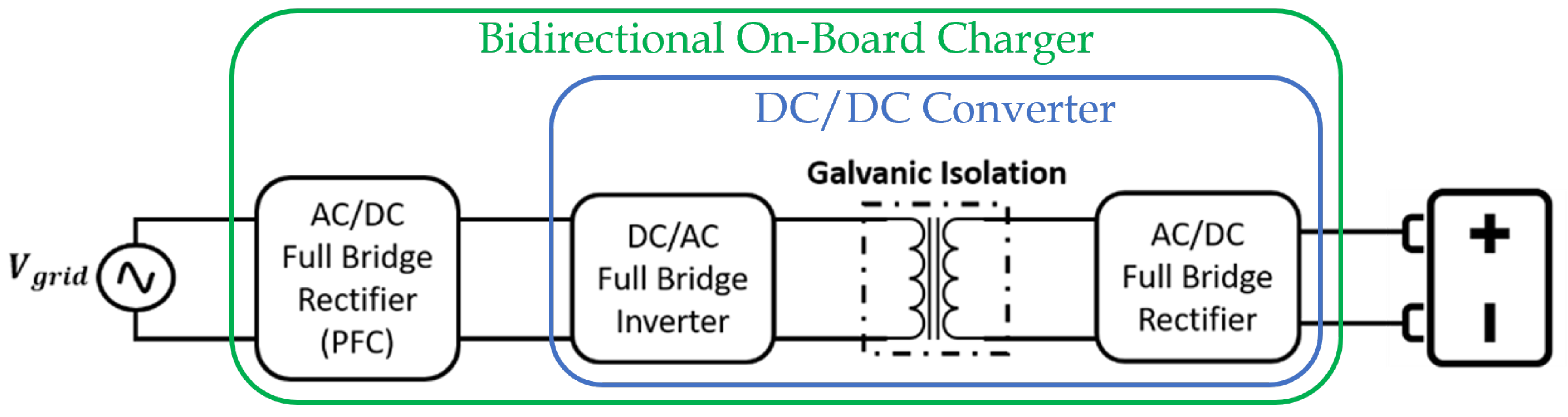
2. On-Board Charger Model and Control

In this study, we consider a circuit architecture composed of several modules, as shown in Figure 1.
In particular, a single-phase bidirectional OBC is considered consisting of an active AC/DC converter followed by an isolated DC/DC converter, which, in turn, consists of a first DC/AC conversion module, a galvanic isolation transformer, and finally an AC/DC conversion module. As reported in Figure 1, the sequence of AC/DC converter, galvanic isolation transformer, and AC/DC stage represent a Dual Active Bridge DC/DC converter. By adding the AC/DC converter, the entire OBC device is defined.

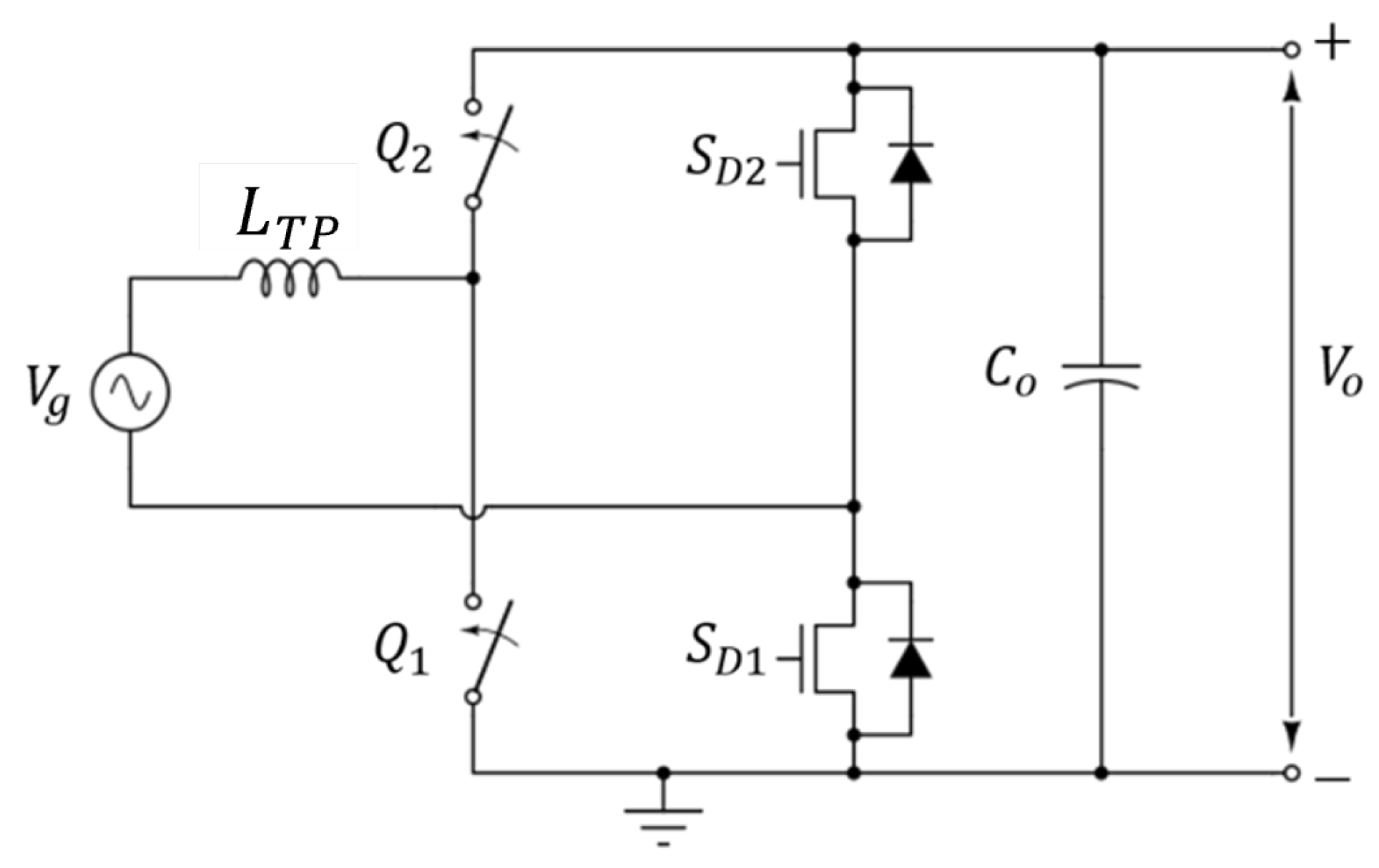
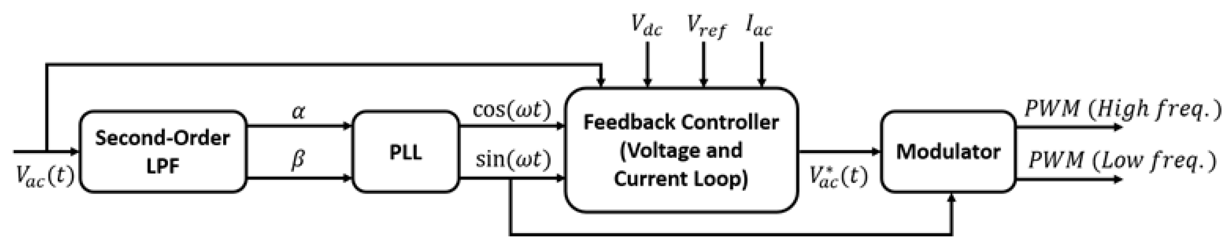
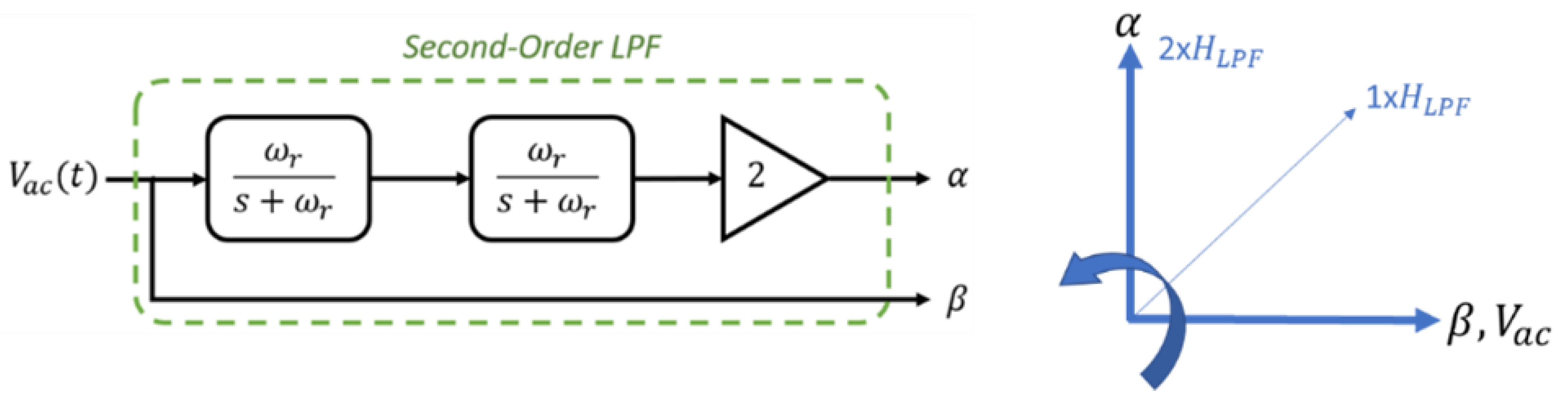
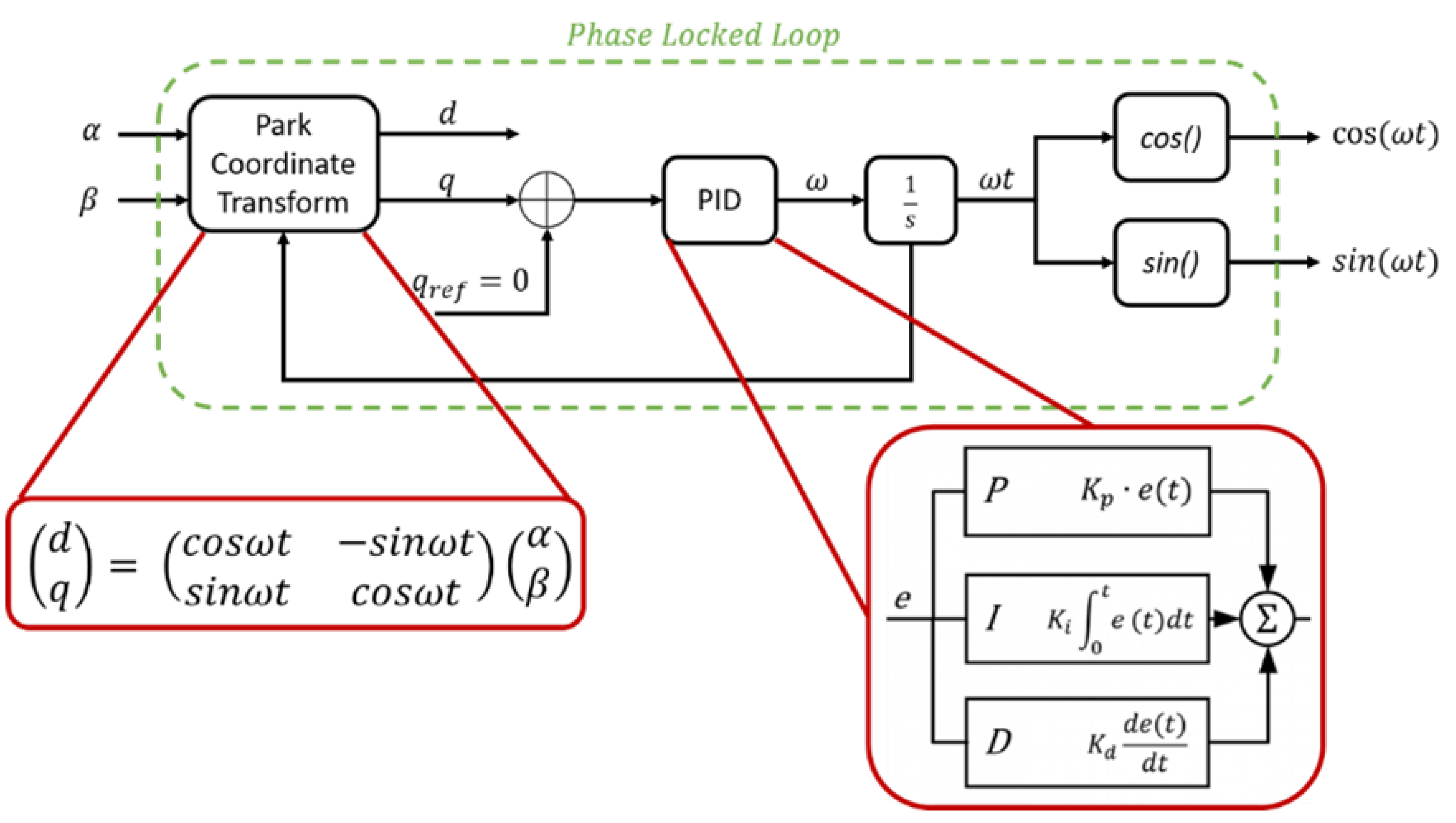
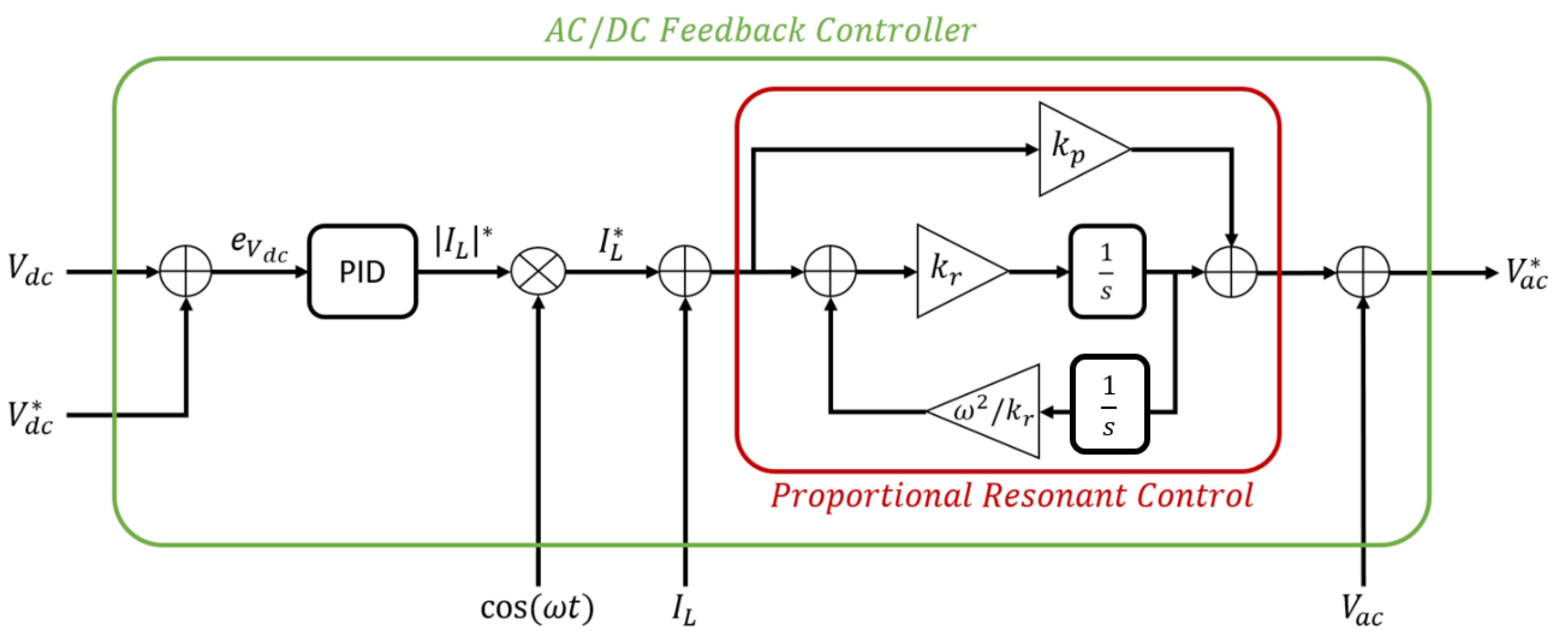
2.1. AC/DC Converter Modelling and Control

We consider an AC/DC conversion module connected to the grid, as shown in Figure 2, of a Totem Pole type. The module is composed of a branch of GaN (Gallium Nitrade) transistors, Q 1 , Q 2 working at high frequencies (typically higher than 200   k H z ) and a branch of transistors working at grid frequency, S D 1 and S D 2 , to achieve current rectification (common power mosfets or IGBTs can be used).
Note that L T P represents the connection to the AC source in the ideal case; obviously the real connection will have to take into account input fluctuations; therefore, an EMI (Electromagnetic Interference) filter has to be inserted. The Totem Pole control is designed to achieve a power factor corrector (PFC) [12], i.e., reactive power minimization. In order to achieve PFC together with DC side voltage level regulation, the control scheme is composed of several functional blocks, as shown in Figure 3.
As schematically shown in Figure 3, the feedback controller handles both voltage and current control by using a cascaded control architecture. Thus, we have an external control loop that handles PFC by direct measurement of V a c and generates a current reference such that the desired voltage V d c is obtained.
Both the input voltage V g r i d and the current flowing in L T P are in a permanent sinusoidal regime. This suggests working in the phasor domain, which is obtained by applying Blondel and Park transforms [13].
As shown in Figure 4, in order to obtain a component in phase and one in quadrature with respect to V a c , a second-order filter is applied. Note that in the single-phase case, this is the equivalent of the Blondel transform.
The α and β components are obtained and processed in the Phase-Locked-Loop (PLL) block, schematised in Figure 5. In PLL, the phase shift angle resulting from Park transformation is stabilised and the harmonic components of the active and reactive parts of the input power are determined. Each of the first-order filters ω r s + ω r introduces an electrical 45° phase shift and an amplitude modulation of 1 2 , which is compensated by a scalar gain.
Figure 6 shows the block diagram of the voltage and current cascade control. The output voltage must be constant; thus, a PI control is used. The current control has to deal with sinusoidal signals; thus, a PR (Proportional-Resonant) controller [14,15] is preferred, characterised by the transfer function in Equation (1).
P R ( s ) = K p + K r s s 2 + ω r 2
We propose the use of current control by means of a Proportional-Resonant (PR) controller instead of the more common Proportional-Integral (PI). The choice is derived from technical reasoning based on the principle of the internal model, which suggests setting up the control in such a manner as to have reference poles in the open chain of the control loop so as to ensure zero error at steady state. At least ideally, the current loop should chase references of type I o c o s ( ω r t ) and as noted by Equation (1), there is the term s s 2 + ω r 2 , which is precisely its L-transform.
The output of the current control is added to V a c to obtain the voltage to be modulated so as to regulate GaN-type devices. The active component, resulting from PLL, is instead processed to modulate devices operating at main frequencies in order to obtain the rectification of the current output from the Totem Pole (see Figure 7).

2.2. DC/DC Converter Modelling and Control

We consider a Dual Active Bridge DC/DC converter with galvanic isolation transformer, for which its circuit is shown in Figure 8.
The control of the DAB consists of regulating the phase shift between the primary and secondary voltage of the transformer [16].
P = n V 1 V 2 2 π 2 f s w L D A B ϕ 1 ϕ π
Equation (2) describes the power supplied by the DAB as a function of the input voltages V 1 and output voltages V 2 , the switching frequency f s w , the value of the coupling inductance L D A B , and the phase shift between the voltages at the ends of the transformer.
ϕ * = π 2 1 1 8 P * f s w L D A B n V 1 V 2 *
By manipulation of the power equation, Equation (3) is obtained, which quantifies the shift according to the input and output voltages. Thus, the shift p h i determines current intensity in L D A B and the mean value of the output voltage.
Figure 9 shows how the variation of the phase shift between the primary and secondary transformer voltage affects the current trend on L D A B , which in fact decides the current trend on the load (due to the rectification of the second active bridge) and, consequently, the voltage on the load. Increasing the phase shift results in increasing the average value of the output voltage. As shown in Figure 10, the duty-cycle is set to 0.5 for both DC/AC and AC/DC modules, and the time-shift between signals P W M H 1 and P W M H 2 is calculated via a PI-type control on the output voltage.
In this paper we consider, Phase-Shift modulation due to its simplicity of implementation, which reduces the number of degrees of freedom for controlling the output voltage to only the phase shift between the primary and secondary voltages, defined by ϕ . Even though there are some inherent limitations, such as the generation of a transformer current with a higher RMS value than other modulation techniques and an operating range in which conduction losses can be neglected that is more limited, it remains the most widely implemented modulation technique in practical solutions, as significantly higher power transfer flows are achieved than with other techniques.

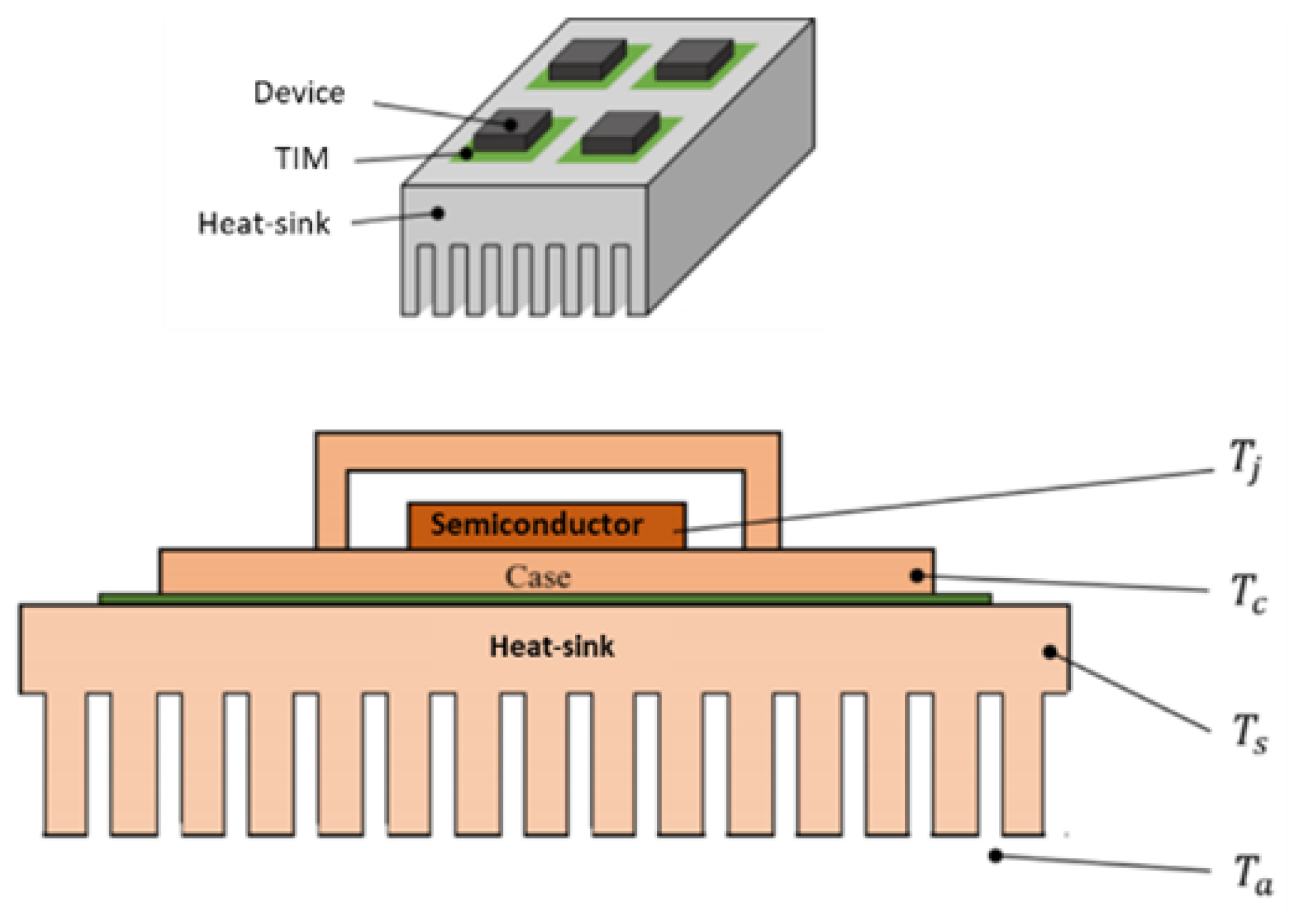
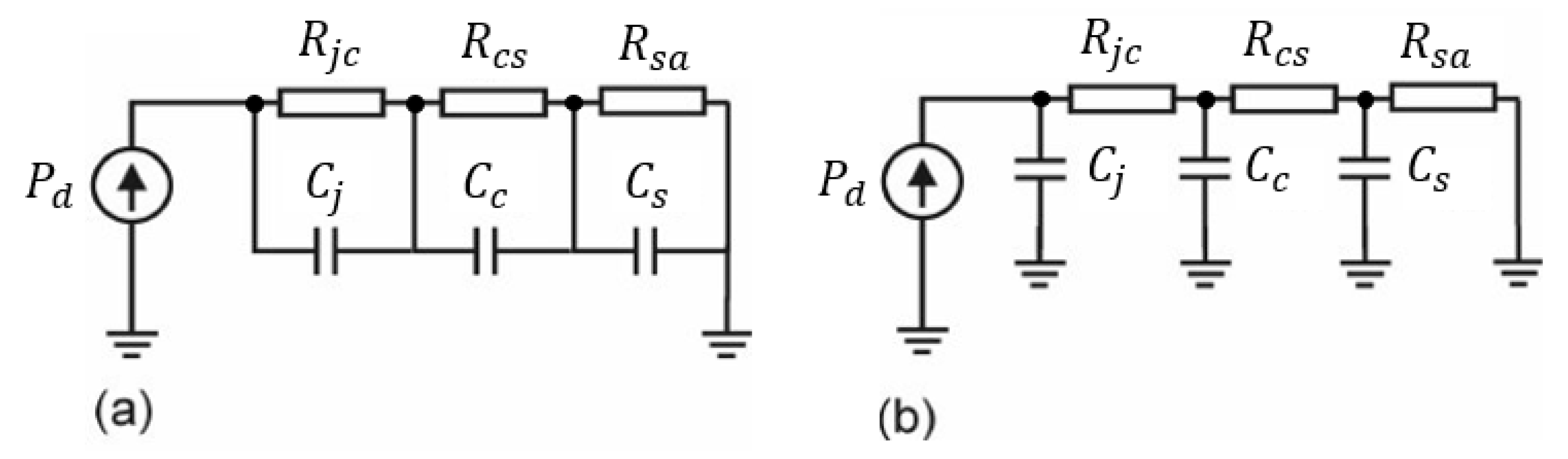
2.3. Thermal Modelling of Switching Devices

In this study, we include a thermal model for switching devices, which takes into account how the device is made and how it is placed in the overall OBC circuit. Such a model must exist in the same simulation environment in which the control systems are validated; thus, its computational complexity must be small.
As shown in Figure 11, we consider a vertical layering of each switching device characterised by a junction (representing the hottest point), the casing, the insulating material, and the heat sink. Figure 12 shows the most common equivalent circuits describing thermal behaviour used in the context of the design of power electronic devices [17].
We denote by R j c the thermal resistance between junction and casing; we denote by R c s the thermal resistance between casing and heat sink; and we denote by R s a the thermal resistance between heat sink and external environment (which we assume to be isotherm). C j , C c , and C s represent the thermal capacities of junction, casing, and heatsink, respectively. In this paper, we refer to Foster’s circuit model (Figure 12a) where we reasonably assume that for each electronic device the chain of mismatches, C j C c C s applies. As a source of dissipated power, we consider, for the sake of simplicity, only the joule effect.

3. Sizing and Selection of Real Devices for Realistic Model-Based Validation

This section recalls the equations necessary for the sizing of passive circuit components and the essential considerations for the sizing and selection of active components with real characteristics. The preliminary specifications for the design of the OBC device are related to the input AC voltage level, the battery side DC voltage range, and then the output from the OBC. Single-phase grid connections were in the main configurations for EU and American standards, with voltage intensity V a c = 110 / 230 Vrms and grid frequency f r = 60 / 50 Hz. The DC bus voltage level, which is output from Totem Pole, is adjustable in the range of 450–800 V. The battery voltage level for the DC-DC converter output is adjustable in the range of 200–400 V. The required output power in the nominal case is P o u t = 7.2 KW.

3.1. Totem Pole

With reference to the Totem Pole circuit, it is necessary to introduce equations for sizing input inductance for the AC side and the output capacitor for the DC side [18]. In particular, inductance plays an important role in affecting system efficiency, current ripple, and overall size. The selection is always a balance between efficiency and power density. The inductance value is calculated based on the input voltage, output voltage, and worst-case ripple. Calculation of the current ripple into inductance can be distinguished into three periods, as reported in Equation (4):
I r i p p l e = T s w L V i 2 V o V i D i f D 1 3 2 V i V o V i D 1 3 i f D 1 3 , 2 3 3 V i D 2 3 i f D 2 3
where I r i p p l e is the current ripple at the Totem Pole input, which is a function of input and output voltages V i and V o , the duty-cycle D = 1 V i V o , the switching period T s w , and the inductance itself. Equation (4) shows the worst-case ripple expression, which is obviously increased by the ripple relative to the maximum AC power and current, from which the inductance selection condition is derived. In Equation (5), P o , m a x is the maximum expected output power, V i , m a x is the maximum expected AC-side voltage, I % is the maximum expected current ripple percentage according to design specifications, and η is the efficiency of the converter, which we can assume is not less than 95%. Assuming a maximum acceptable current ripple of 10% and the values related to the preliminary specifications, we obtain that the minimum value of the input inductance at the totem pole is L m i n = 113 μ H.
I r i p p l e , w o r s t = V o T s w 12 L < I % 2 P o , m a x V i , m a x η
Due to the input double-line frequency ripple on the DC link capacitor, its capacitance is mainly determined by the output voltage ripple (see Equation (6)), where we indicate P o as the output power, V o is the output DC voltage, f l i n e , m i n is the minimum grid frequency, and V r i p p l e is the maximum voltage ripple derived from project specifications.
C o P o 4 π f l i n e , m i n V o V r i p p l e , m i n
Considering initial specifications, the minimum value of capacitor that can be obtained through the last expression is C o , m i n = 260 μ F.

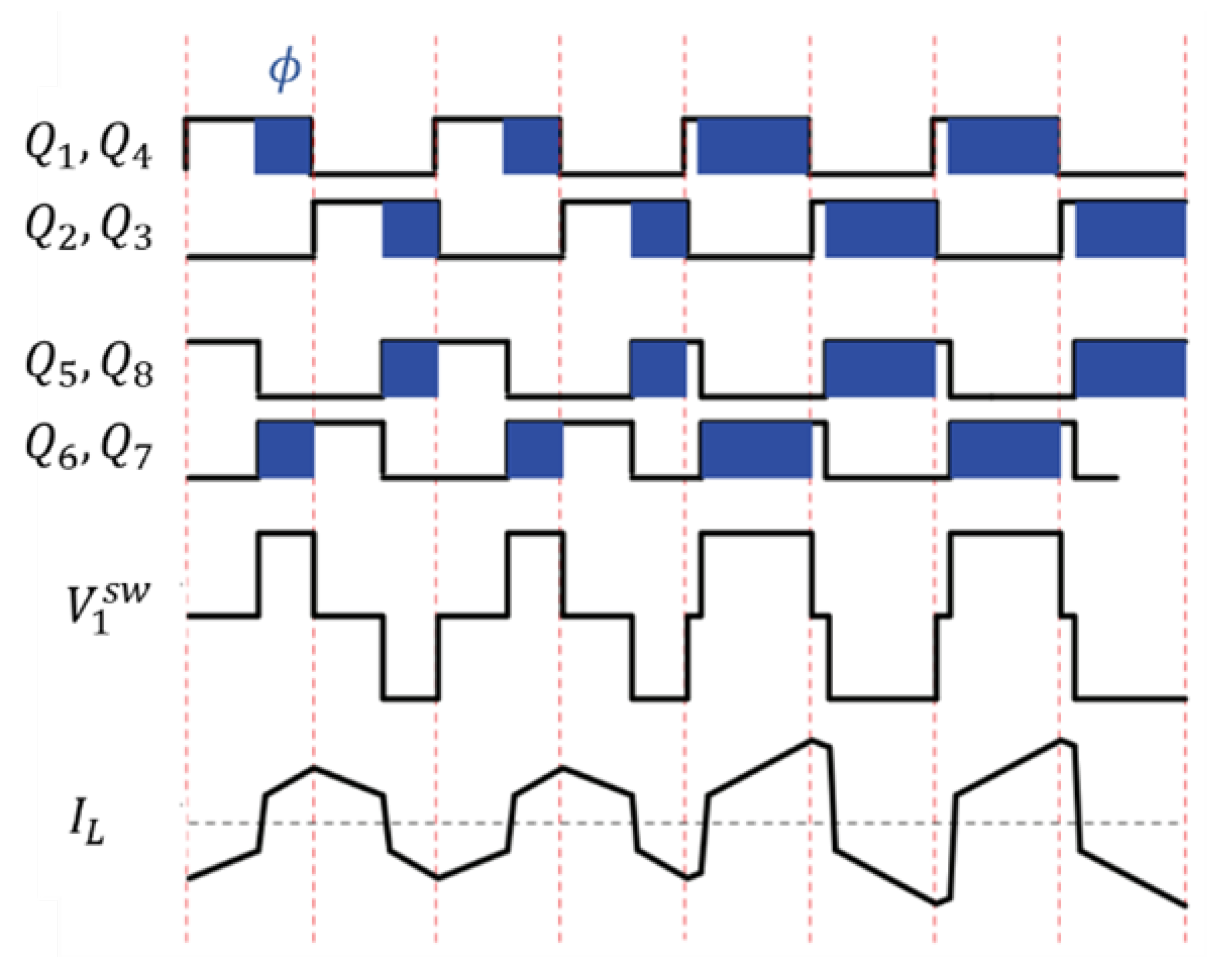
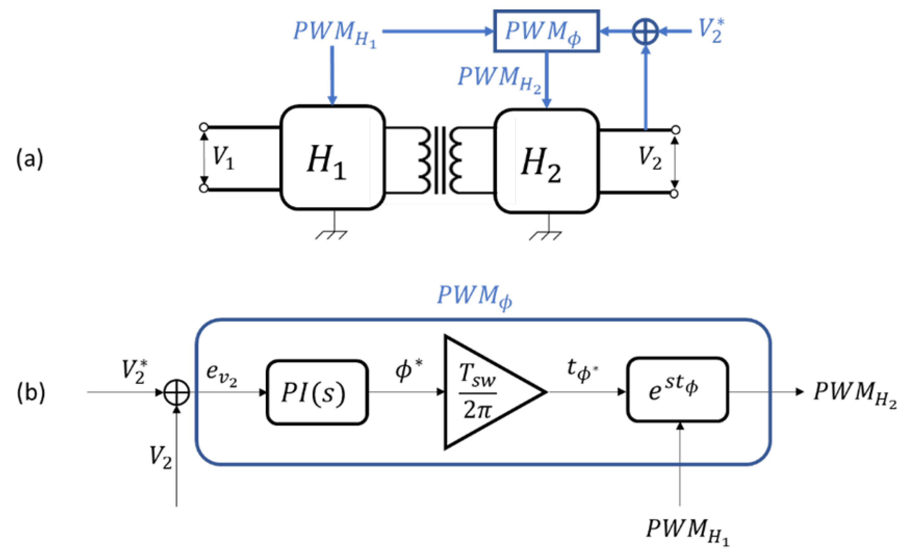
3.2. Dual Active Bridge

With reference to the DAB DC-DC conversion circuit, sizing expressions for inductance on the primary side of the transformer and the capacitor on the DC output side must be derived [19]. Equation (7) represents the primary-ended inductance selection condition of the DAB transformer, where voltages V 1 and V 2 are the input and output DC voltage levels, respectively, P o , m a x is the maximum expected output power, and f s w is the switching frequency. Considering the specifications, the value of the minimum required inductance is L t o t , m i n = 117 μ H. Regarding the sizing of the output capacitor, it serves mainly to absorb output voltage ripple (battery side); thus, it is necessary to describe electrical balance, then the dynamics of the voltage at the ends of the capacitor, as reported in Equation (8).
L o u t η V 1 V 2 8 π P o , m a x f s w
C o d V 2 d t C o V 2 , r i p p l e D T s w = V 1 2 π f s w L t o t ϕ 1 ϕ π V 2 R l o a d
Similarly to how we derived the L t o t condition of choice, we consider the expression for maximum power transfer, with ϕ = π 2 , and consider the expression for d V 2 V 2 , r i p p l e and d t D T s w in order to quantify the derivative with incremental rapport in the conduction phase. R l o a d indicates load resistance, which can be expressed in a first approximation as the ratio of the power to the output voltage. In addition, all maximum values of voltage and power are considered. Thus, we obtain the condition for the choice of the capacitor, as in Equation (9).
C o D T s w V 2 , r i p p l e V 1 , m a x 8 f s w L t o t P o , m a x V 2 , m a x
For what concerns the choice of MOSFETs, both GaN and SiC, it is necessary to derive the conditions regarding the voltage between drain and source V d s and the drain current circulating in the devices during conduction I d . Thus, we have to consider the starting specifications related to output power P o u t , output voltage range V o u t ( V d c , m i n , V d c , m a x ) , and peak supply voltage on AC side such that we can have V A C ( t ) = V a c s i n ( 2 π f r t ) with V a c ( V a c , m i n , V a c , m a x ) in rms values. The minimum value of the output capacitor due to the specification is C o , m i n = 120 μ F.

3.3. Switching Devices

A preliminary sizing of the MOSFETs can be performed by considering a safety margin μ with respect to the maximum voltage and the maximum current expected on each branch of the active converters, as provided in Equation (10).
V d s , m a x ( 1 + μ ) V d c , m a x I d s , m a x ( 1 + μ ) P o u t V a c , m i n
Note that I d , m a x means the pulsed drain current and not the continuous drain current, which is obviously much lower. The values obtained according to the introduced specifications, considering a safety factor μ = 15 % , are V d s , m a x 900 V and I d , m a x 50 A. With these specifications, we have selected the following electronic devices to meet the conditions calculated by using following sizing methodology:
  • TP90H050WS 900V Cascode GaN FET in TO-247 [20];
  • NTBG040N120SC1 1200 V SiC Power, Single N-Channel, D2PAK-7L [21];
  • STTH1210 Ultrafast recovery-high voltage diode [22].
The characteristics and values of the internal parameters of these devices were considered in the simulation environment. In the next section, the simulation results obtained for both voltage and current regulation using classic controllers and thermal behaviour are exposed.
Note that Table 1 shows the values of the passive elements (basically inductance and capacitor of Totem Pole and DAB converters) obtained from sizing expressions. Moreover, the characteristics of the switching devices selected according to the design specifications are also shown and are taken from their data sheets. Considering the characteristics of real devices allows us to exhaustively simulate the electrical and thermal behaviour of the converters that make up the OBC topology. With regard to the choice of transformer, we have referred to products for automotive applications with comparable power levels. In particular, in [23], we refer to the design procedure of a DAB for powers of about 6 kW, input voltages of 700–800 V, and output voltages of 380–500 V. In Table 2, the isolation transformer features we use for realistic simulations are summarized.

4. Simulation Analysis

First we present simulation results for voltage and current control in totem pole and dual active bridge converters, taking into account different operating ranges both in terms of the desired output voltage from the converters and the AC source. The thermal analysis of the switching devices in the two converters is then presented, taking into account an “intermediate” operating condition. Finally, the robustness analysis to parametric variations is presented for the voltage and current control of the two converters, in order to validate the robustness of the control loops to modelling uncertainties.

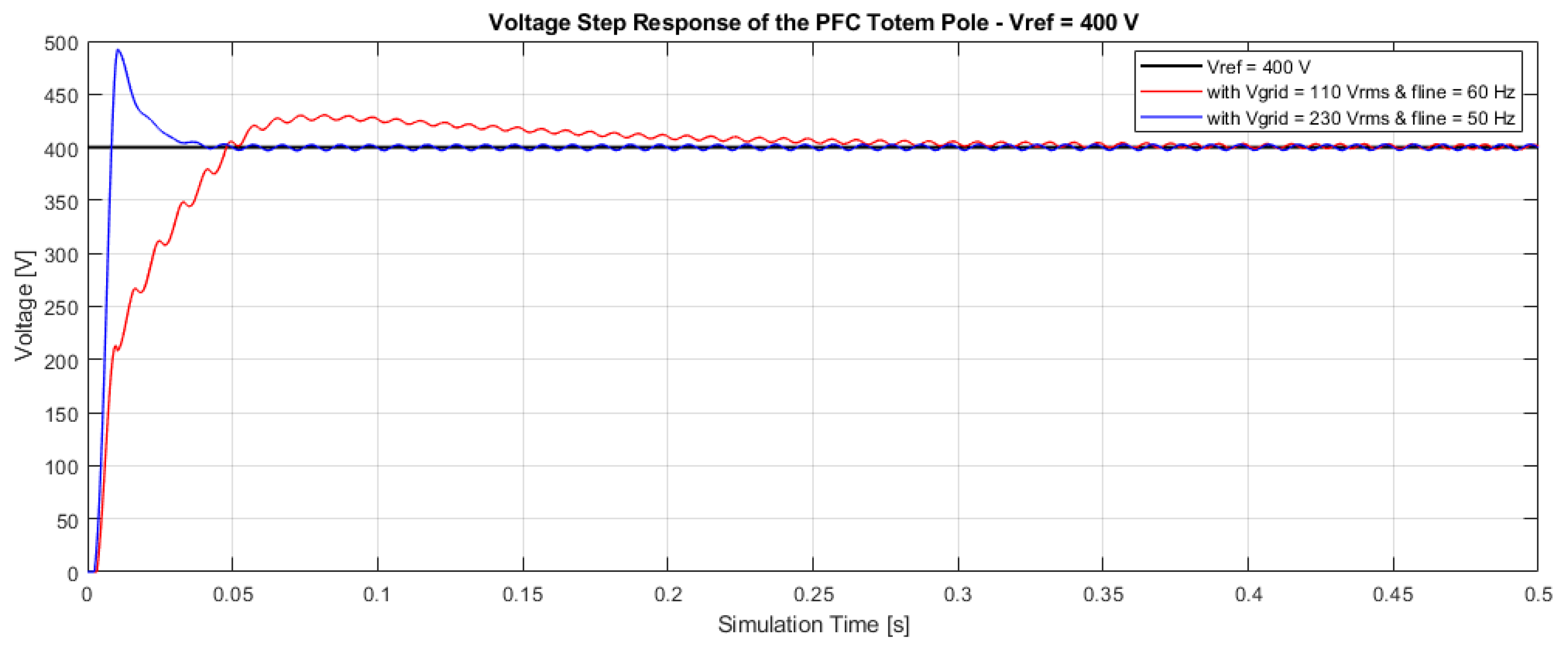
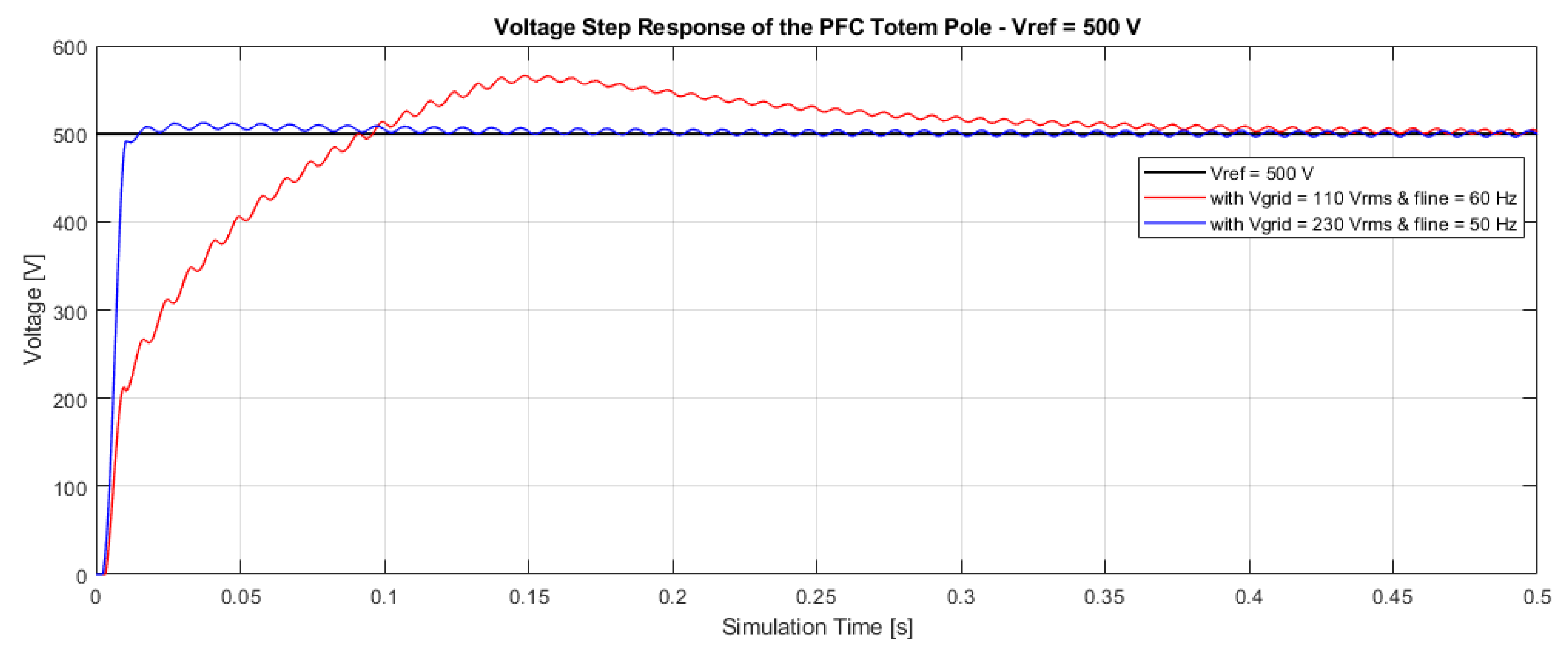
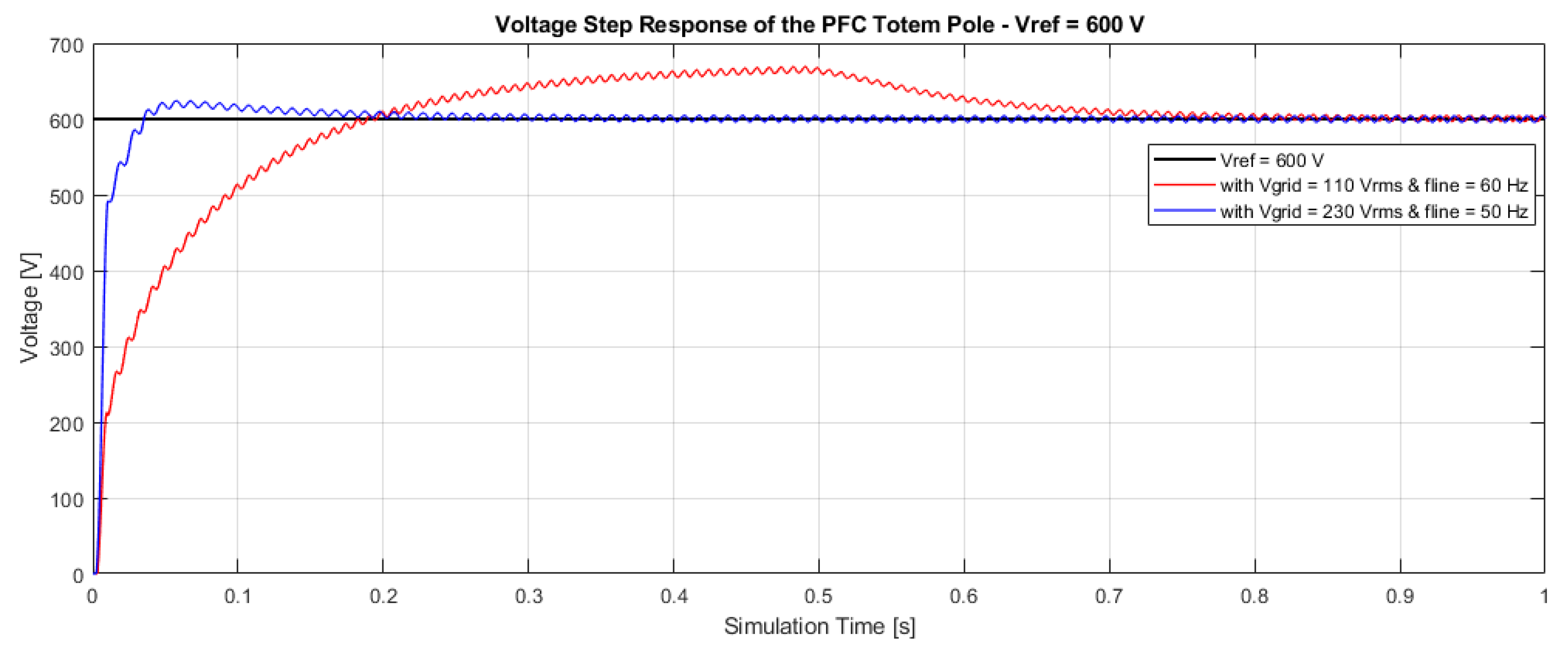
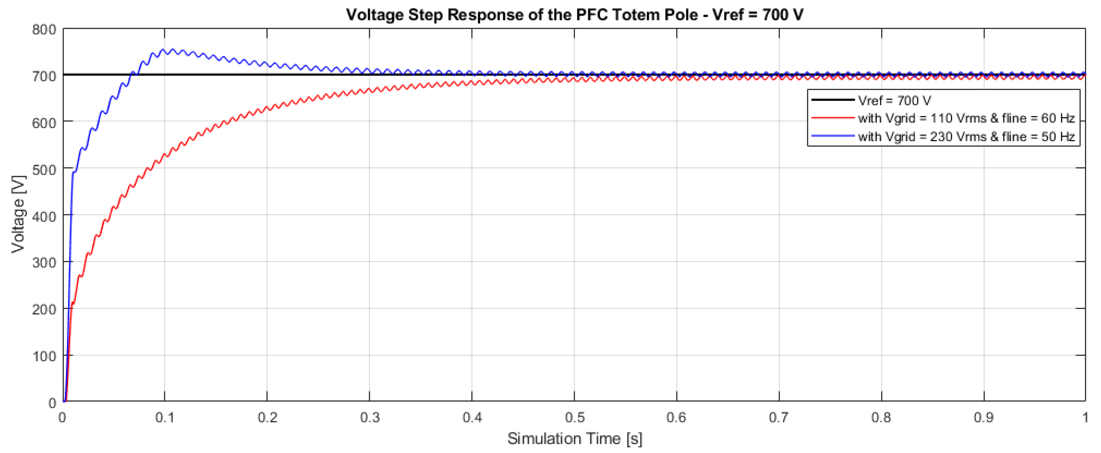
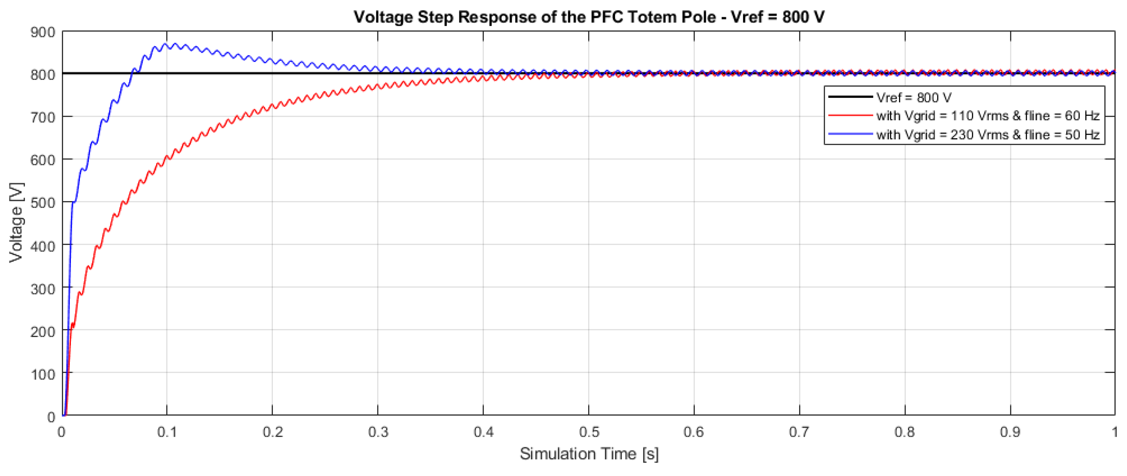
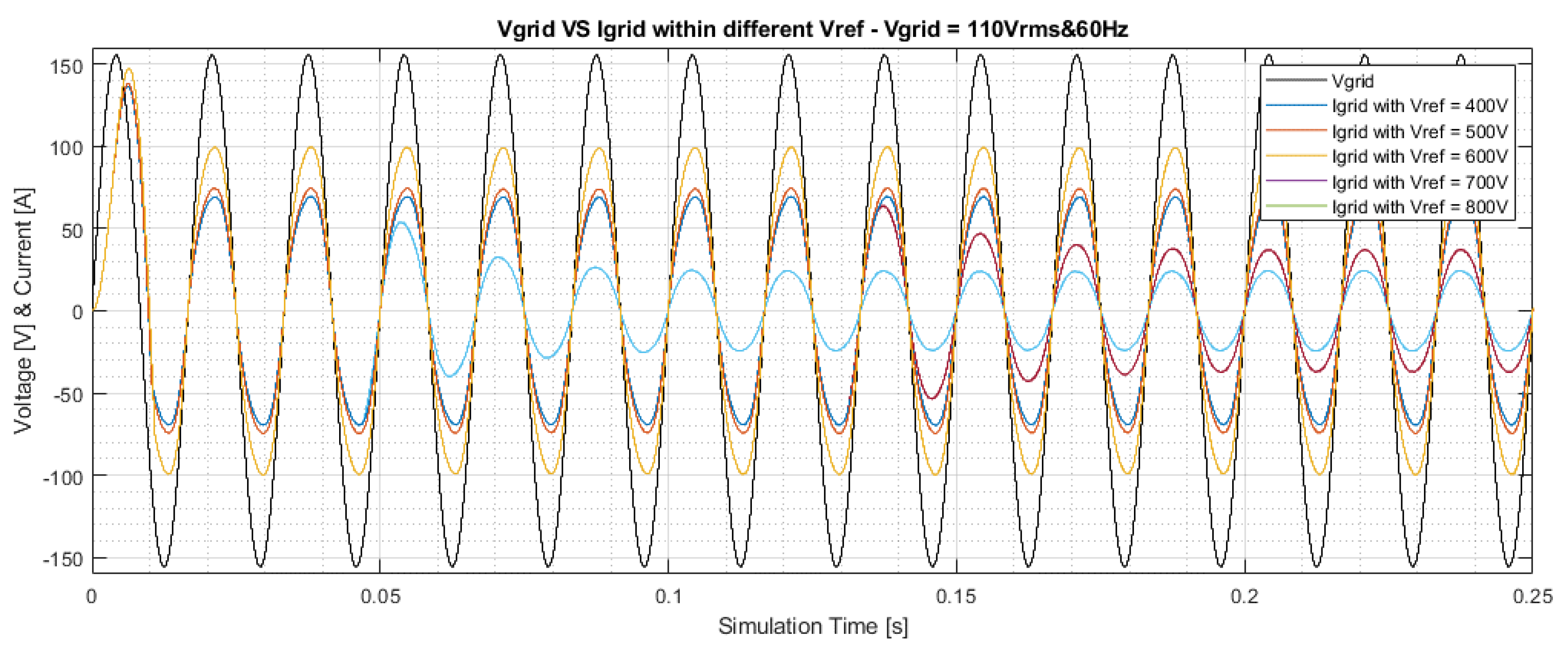
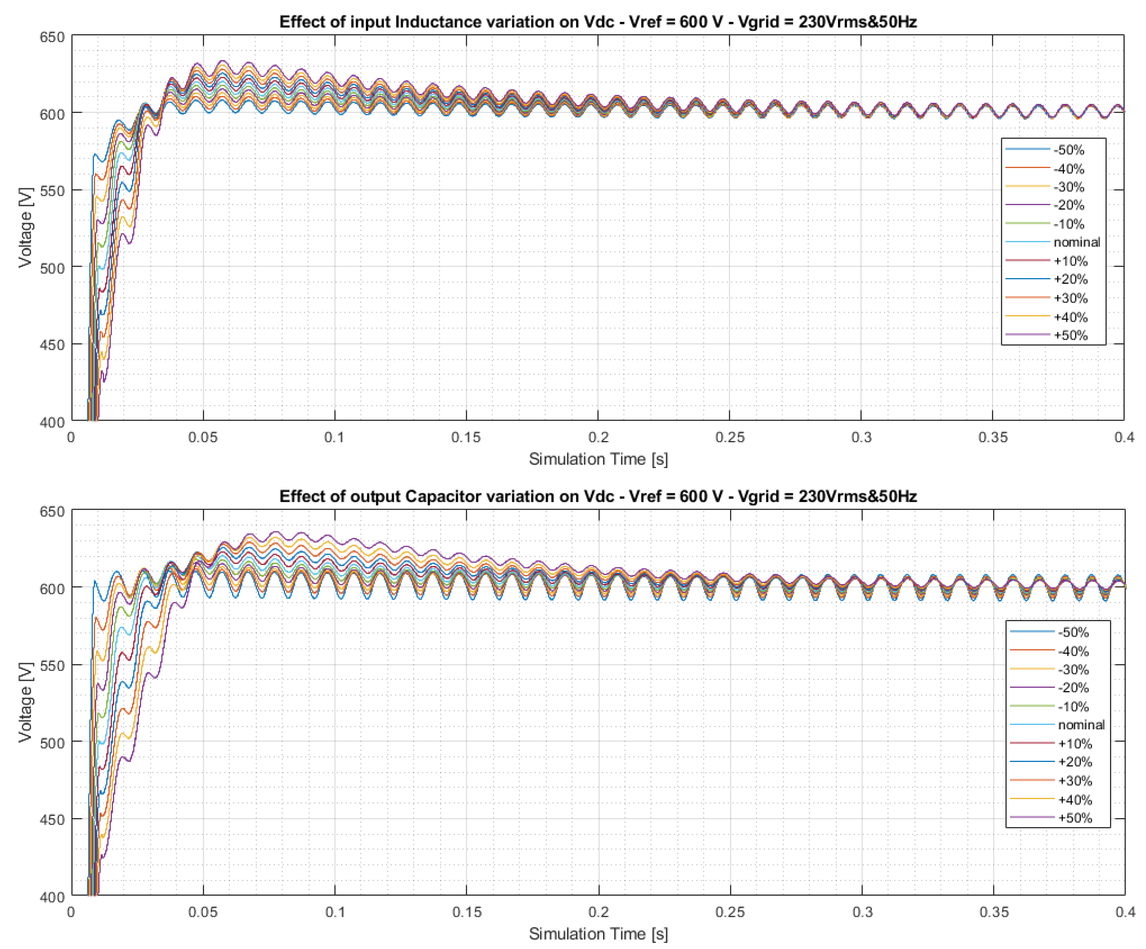
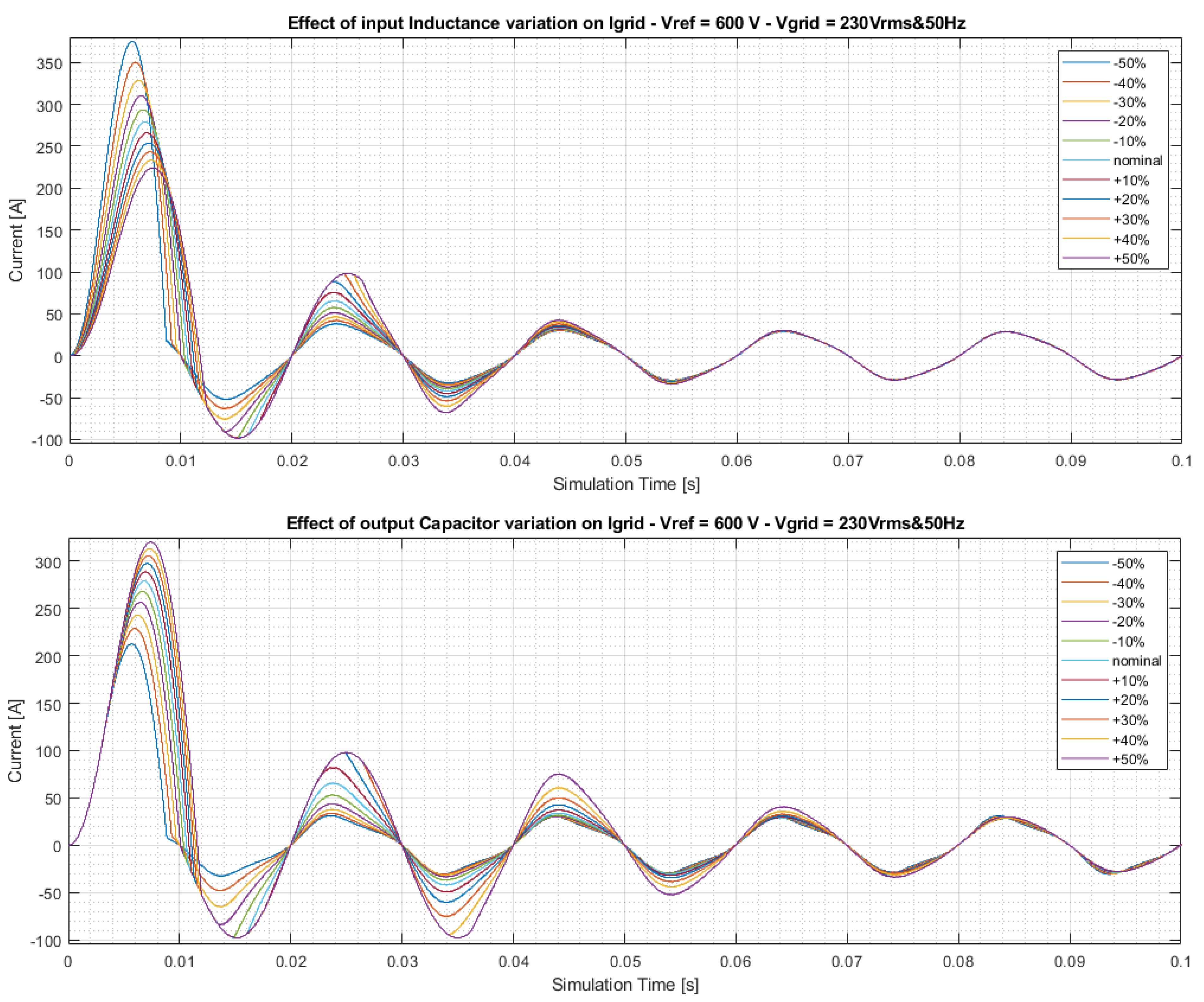
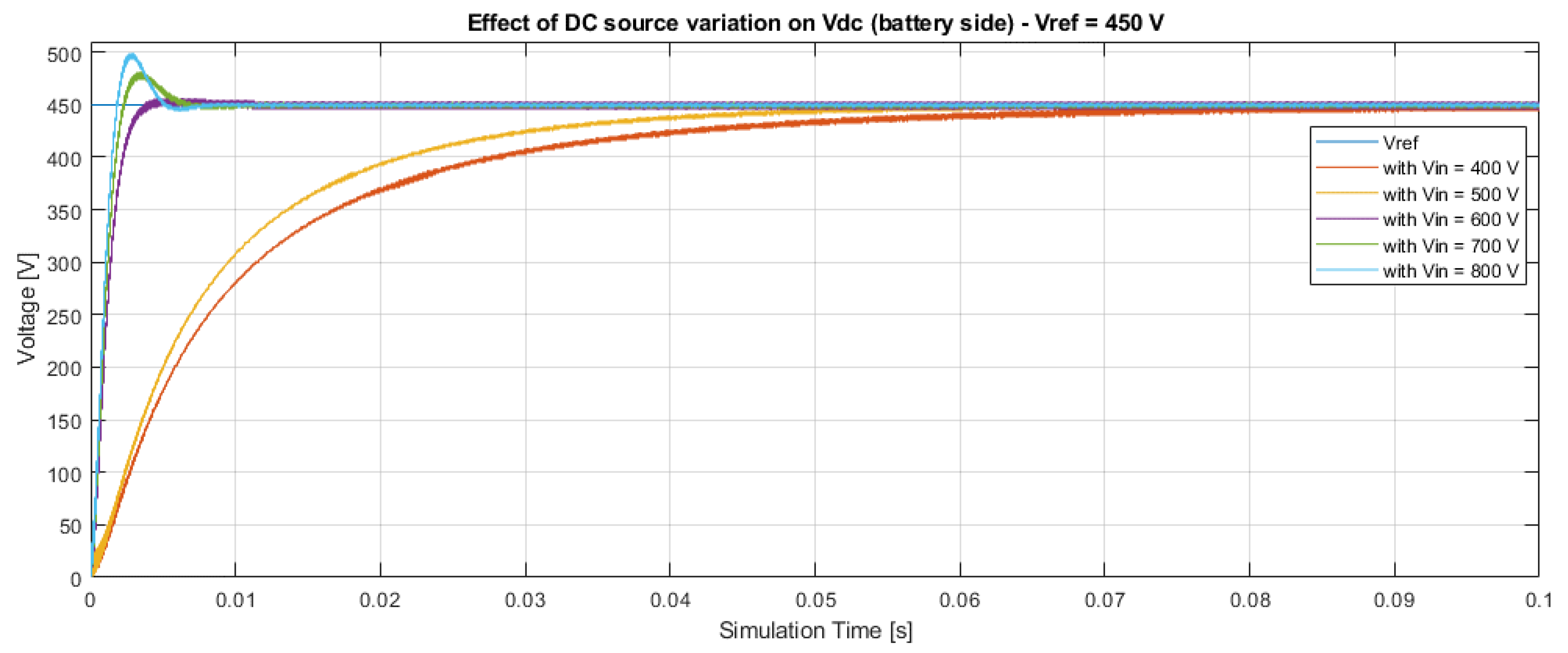
4.1. Control of the Totem Pole Converter

Figure 13 shows the result of voltage control of the totem pole converter when the required DC bus voltage is 400 V. The results obtained with different AC side source are compared. For this operating condition, in the case where the source is 230 Vrms and 50 Hz, the converter behaviour is characterised by a high overshoot (almost 20% with respect to the steady-state value) but with very fast rise and settling times ( t r i s e 0.01 s and t s e t t l i n g , 5 % 0.03 s). In the case of an AC source with 110 Vrms and 60 Hz, the behaviour of the output voltage is increasingly “ smooth,” with a much smaller overshoot (about 7.5% with respect to the steady-state value), with longer jumping and settling times ( t r i s e 0.04 s and t s e t t l i n g , 5 % 0.15 s) that remain, however, decidedly acceptable for this type of application.
In Figure 14, a different result was obtained with respect to the previous one. The case with AC source 230 Vrms and 50 Hz has a behaviour practically of the first order, with an overshoot lower than 2.5% with respect to the steady-state value and with both rise and settling time of about 0.01 s. In the case of a 110 Vrms and 60 Hz AC source, on the contrary, a second-order behavior was obtained with an overshoot of about 13% with respect to the steady-state value and with looser dynamics, characterized by a rise time of t r i s e 0.07 s and settling time of t s e t t l i n g , 5 % 0.03 s.
Figure 15 shows the control result in the scenario where the voltage reference is 600 V. In the case with 230 Vrms and 50 Hz, there is a behaviour with reduced overshoot (about 4.2% of the steady state value) and quite contained rise and settling times ( t r i s e 0.002 s and t s e t t l i n g , 5 % 0.1 s). With AC source 110 Vrms and 60 Hz, there is a second-order behaviour again with an overshoot of about 11.5%, rise time of t r i s e 0.15 s, and settling time of t s e t t l i n g , 5 % 0.8 s.
In Figure 16 and Figure 17 are shown the results obtained for a required DC voltage level of 700 V and 800 V, respectively, within variation of operating condition as reported for the previous cases.
Table 3 summarises the results obtained in terms of voltage step repose for the Totem Pole circuit under the different operating conditions ( V g r i d and f l i n e ; V r e f ).
Figure 18 and Figure 19 show the current trends I g r i d in various scenarios with different AC source V g r i d and different reference voltage V r e f .
The purpose of current control, in a Totem Pole converter, is to phase the current with respect to the supply voltage (AC side); thus, the desired graphical result is to have V g r i d and I g r i d , which are two harmonics that are perfectly in phase (different amplitude of course).
As observed from the simulations, the implemented control scheme is able to compensate for the phase shift between voltage and current in order to obtain power factor correction (PFC). In fact, in all scenarios analysed, after an initial phase of limited time duration (in the worst case 0.03 s) in which the two electrical quantities are out of phase, there is a perfect synchronisation and eventual subsequent adjustment to the steady state value.
It should also be noted that the simulations are consistent with the choices made when sizing the switching devices both in terms of the peak current that can be sustained and the intensity during continuous operation.
The following is a robustness analysis of the Totem Pole voltage and current control with respect to the variation of circuit parameters. This type of analysis is quite important for evaluating the tuning of the control parameters since real components are always affected by measurement uncertainties; thus, it is always good practice to evaluate the quality of the control in the presence of uncertainties with respect to the nominal model.
In Figure 20, the transient of the Totem Pole voltage control is shown when varying the value of input inductance on the AC source side (upper) and when varying the output capacitor on the DC bus side (lower). It can be observed that the control is robust in both cases within a reasonable range of variation ( ± 50 % ). In particular, as output capacitance decreases, residual ripple increases due to the fact that a lower capacitance can “absorb” a lower charge in the conduction phase.
Figure 21 shows the effect of parameter variation on the grid current. It can be noted that in the steady-state phase, the variation of those parameters has a very low effect, while in the transient phase, the peak of current value changes considerably. This kind of analysis can support the design phase in order to reconsider the choice of device with higher peak of current.

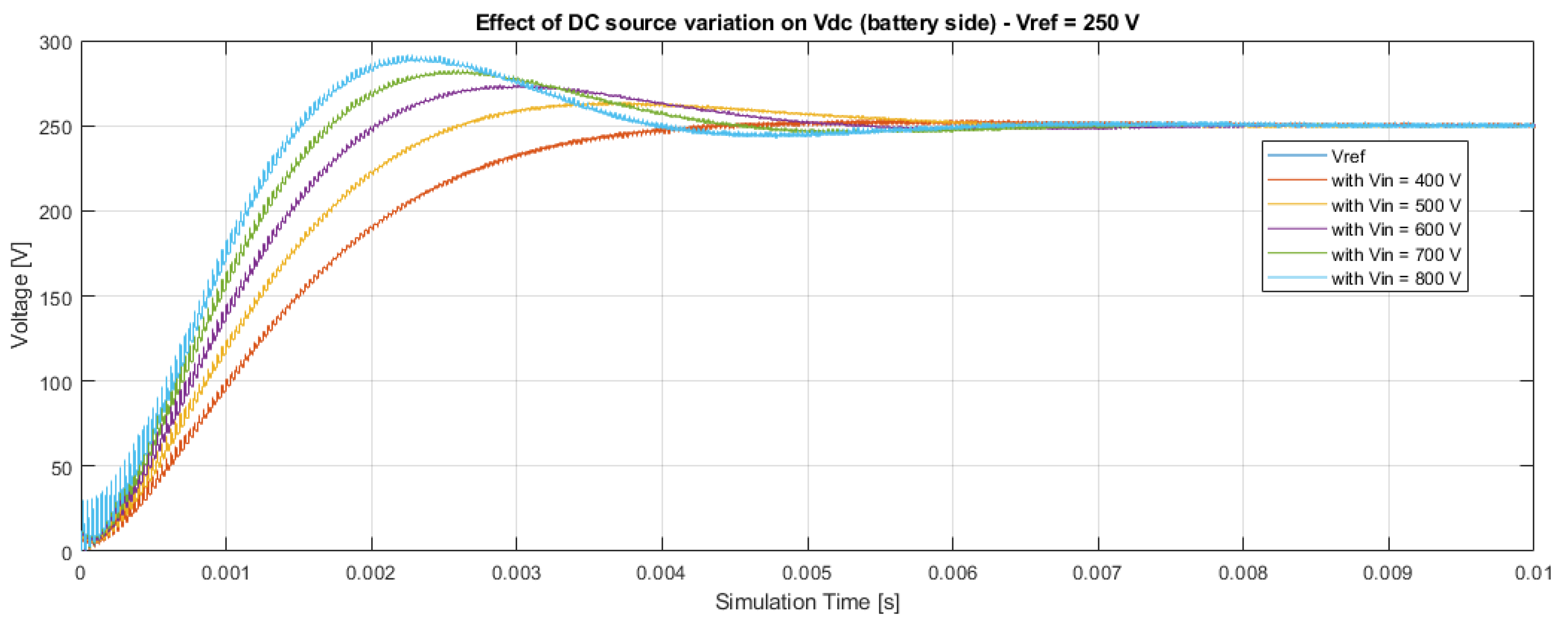
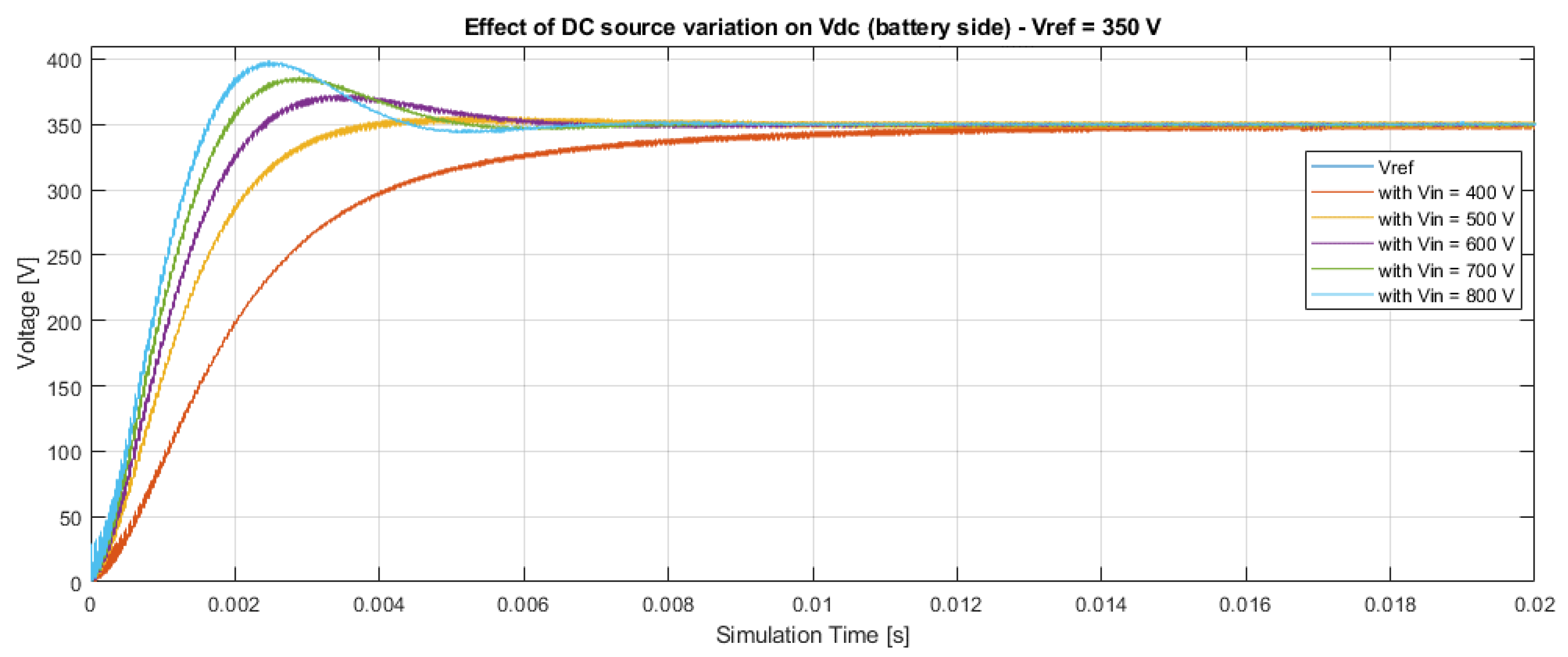
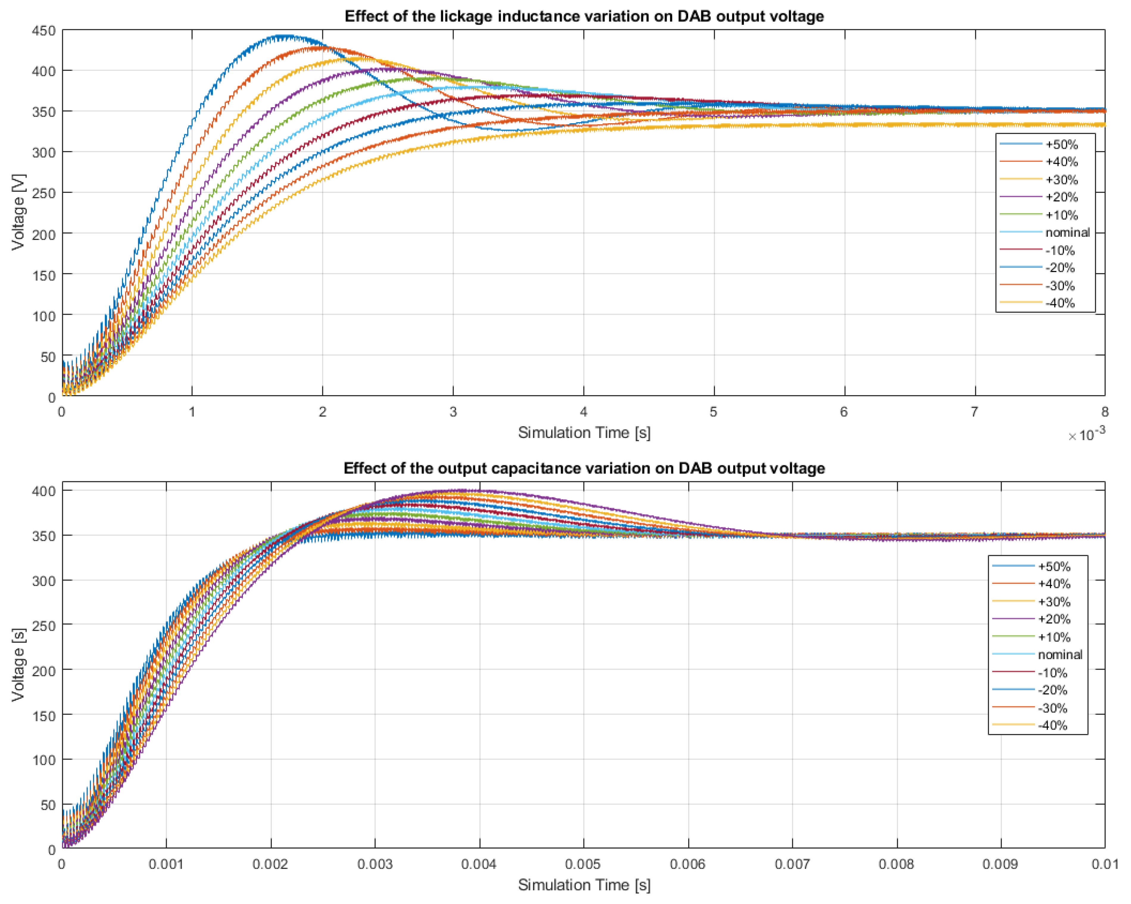
4.2. Control of the Dual Active Bridge Converter

The output voltage control of the DAB is presented below. As discussed in the specification, the output voltage should be adjustable, as required, in the range of voltage values V d c [ 250 , 450 ] V, similarly to how the DC bus voltage at the input to the DAB (which is the voltage value provided by the Totem Pole) can vary in the range of values V i n [ 400 , 800 ] V. Some combinations between V r e f and V i n are proposed to verify the robustness of the voltage control to variations in the voltage source, since from an algorithm development point of view V i n represents a constant exogenous input to the control loop and, as such, the controller must be able to compensate for its variations (within reasonable operational limits).
Figure 22 shows the variation of the response of the DAB converter as the voltage source (Totem Pole side) changes when an output voltage (battery side) of V r e f = 250 V is obtained. It can be observed that as the input voltage V i n supplied to DAB decreases, the system tends to behave more similarly to a first-order system. In fact, higher V i n corresponds to faster rise times with overshoots greater than the steady-state value.
A similar situation is shown in both Figure 23 and Figure 24, which show scenarios with V r e f = 350 V and V r e f = 450 V, respectively, as V i n varies. It can be observed that as the required V r e f increases, a reduction in the input source becomes more and more relevant. This type of analysis helps not only to verify the robustness of voltage control but also to evaluate which combinations of V r e f and V i n tend to stress the device. In particular, it can be observed in the case where V r e f = 450 V that with input voltages V i n = 400 / 500 V, the converter takes much longer to supply the required voltage level.
In the following, a further robustness analysis is proposed with regard to the variation of circuit parameters. This analysis is important in order to verify that the control is able to stabilise the system even when it does not coincide perfectly with the nominal model. The analysis of robustness to parametric variations is presented with reference to the ’intermediate’ operating conditions both in terms of the input voltage supplied (Totem Pole side) and reference voltage required at the DAB output; thus, the following graphs were obtained with V i n = 600 V and V r e f = 350 V.
Figure 25 shows the trend of the output voltage from the DAB converter (battery side) considering the variation of circuit parameters. In particular, it can be observed (upper) that excessively high values of coupling inductance of the galvanic isolation transformer accentuate the second-order behaviour of the system, considerably increasing the overshoot and also settling time. Smaller values of the coupling inductance, on the other hand, tend to make the system first order, with the drawback that values that are far too small compared to the nominal case can also result in steady-state errors in voltage step response. It can be observed that the system is less sensitive to variations in parallel output capacitance.

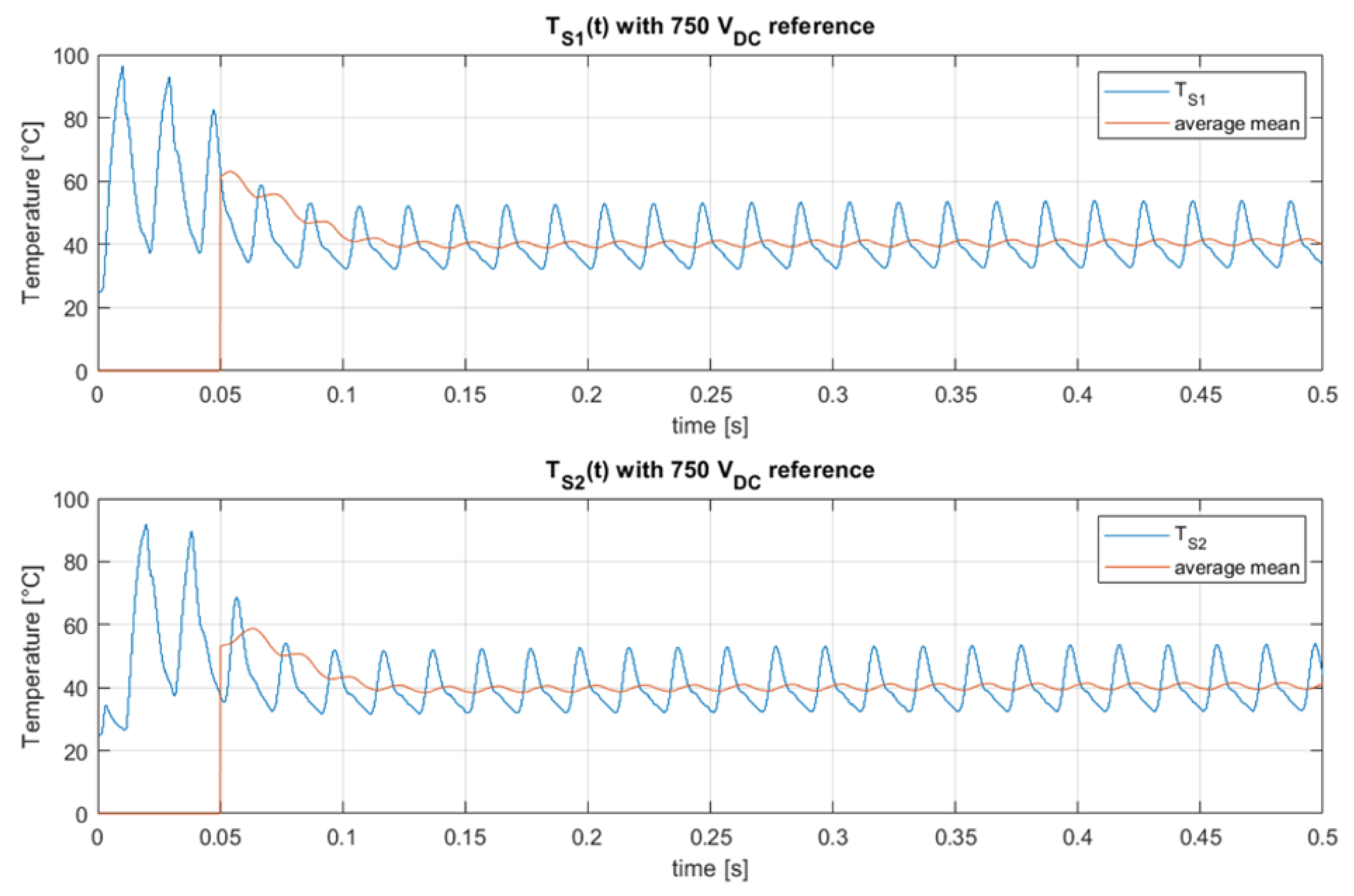
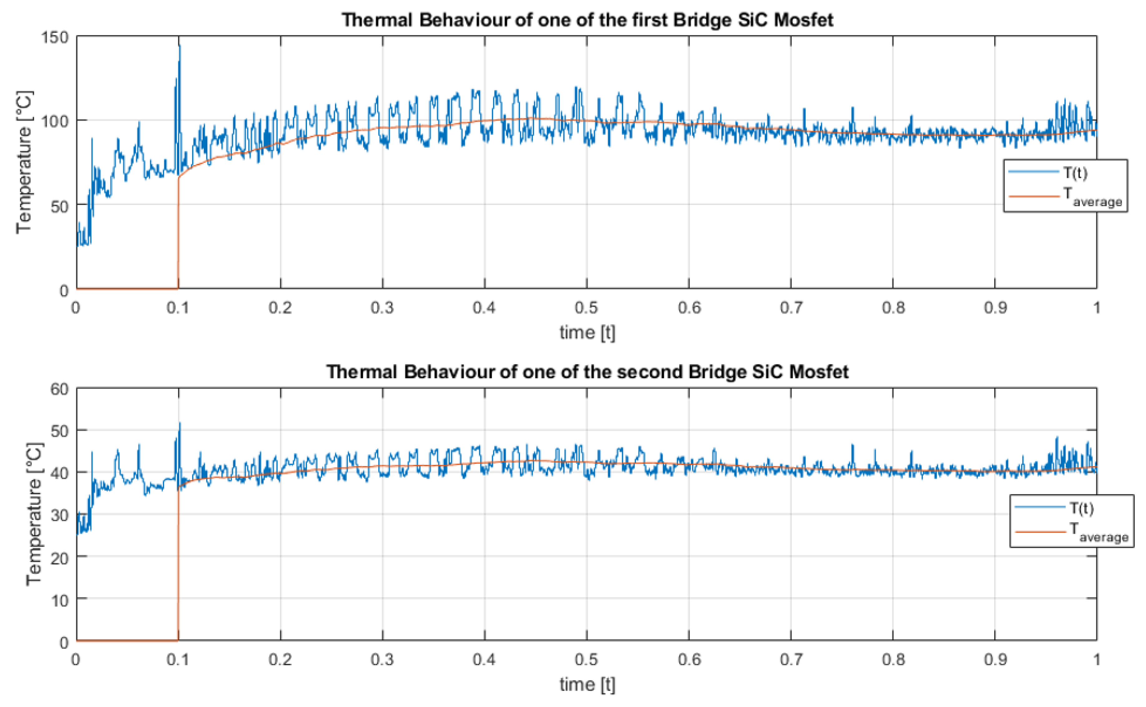
4.3. Thermal Behavior

The simulation results of the thermal behaviour, in terms of the junction of the switching devices, are shown below.
Figure 26 shows the dynamics of the junction temperature of the GaN-type mosfets of the Totem Pole converter. Consistent with the choice of real devices discussed above, the peak temperature can reach no more than 150 °C, and in continuous operation it tends to be below 80 °C. Note that this result is relative to the intermediate operating condition used for parametric robustness analysis.
Figure 27 shows the thermal behaviour of SiC-type devices in the Totem Pole converter. As expected, the average temperature of SiC-type mosfets is lower than that of GaN-type ones, since they operate at much lower frequencies. Moreover, in this case, the simulation is congruent with the choices made when choosing real reference devices.
The thermal behaviour of the SiC devices comprising the DAB converter is shown in Figure 28. In both cases, the average temperature under continuous conditions remains within the declared limits of the data sheets of the real reference devices as well as the peak temperature of the junction remains below 150 °C. It can be observed that the devices in the AC/DC conversion module reached much higher temperatures than those in the AC/DC module. This could be due to the presence of the transformer, which in fact creates an insulation and prevents a continuity of current that results in different temperature ranges. Similar values were obtained in the other operating conditions analysed in the evaluation of the robustness of control algorithms.

5. Results Discussion

The obtained simulation results are very realistic due to the fact that we considering real device features by using reference data sheets and application notes of real commercial power converters [23,24]. The results obtained are certainly in line with those derived from bench measurements of real devices, designed for applications and specifications practically identical to what has been considered here. We have presented simulation results under various operating conditions of practical interest to highlight the fact that the models we use to simulate the converters behave consistently with real systems. For example, the different types of transient when varying the AC source and DC voltage reference in the Totem Pole PFC cause a change in behaviour similar to the voltage step response for second-order system relative to that of the first-order system, depending on the combination of values. Another check of the reliability of the results obtained is in terms of the current absorbed by the Totem Pole converter, in which the almost perfect phasing of I g r i d with V g r i d is obtained at the variation of the operating combinations and at the variation of parametric uncertainties, which actually affected the transient phase in which the highest current values occur. However, these current values remain within the Safe Operating Area declared in the data sheets of the SiC/GaN switching devices selected according to the criteria discussed above. Similar considerations can be made with regard to the thermal behaviour simulated by the equivalent models used, in which device junction temperatures are obtained with typical values, less than 100 °C on average in continuous conditions, and never above the operating limits declared in the reference data sheets.

6. Conclusions and Future Work

This study proposes an operational flow for modelling conversion modules in the context of a modern circuit architecture for onboard chargers in electric and hybrid cars. The operating principles have been described in detail to derive expressions for the sizing of the circuit components of both the Totem Pole and the Dual Active Bridge isolated converters. The control system for the two conversion stages has been described in detail and real devices have been selected that are congruent with the sizing procedure of passive and active components so that the quality of the simulation results can be verified in terms of compliance with the operating limits declared in the data sheets.
Simulations were shown in terms of voltage and current control of the two converters, proposing an exhaustive analysis of the possible scenarios in terms of the different operating conditions of practical interest. Simulations for verifying robustness relative to parametric variations were also proposed as further support for the validity of the results obtained. The added value of this study was to correlate the simulation of electrical and thermal quantities in a single simulation environment without having to use advanced tools such as finite element analysis. By integrating the circuit model and the thermal model in the same simulation environment, it is possible to quickly check whether the voltage and/or current control specifications are such that the thermal limits of the devices are respected. This would not be possible in a simulation with finite element analysis tools since, in this case, thermal and electrical models do not coexist in the same numerical simulation environment.
In addition, having a model that incorporates most of the physical phenomena of interest from a design point of view makes it possible to evaluate different scenarios and different combinations of parameters in a limited number of simulations, while also incorporating issues related to failure analysis by evaluating prediction logic and/or maintenance of the device. This type of analysis represents a development of this study, in which the use of advanced control techniques, such as Model Predictive Control, to improve energy efficiency aspects is evaluated. Furthermore, the development of a model that is both accurate and not too computationally burdensome allows the development of Predictive Health Maintenance techniques based on modern machine learning and artificial intelligence paradigms.

Author Contributions

Conceptualization, S.S. and P.D.; methodology, S.S. and P.D.; software, P.D.; validation S.S. and P.D.; writing—original draft preparation, S.S. and P.D.; writing—review and editing, S.S. and P.D. All authors have read and agreed to the published version of the manuscript.

Funding

The work has been partially supported by MIUR Project “Dipartimenti di Eccellenza” and by the ECSEL JU project Hiefficient n. 101007281 (EU ECSEL-2020-2-RIA call).

Conflicts of Interest

The authors declare no conflict of interest.

References

  1. Xu, R.; Fang, W.; Liu, X.D.; Liu, Y.; Hu, Y.; Liu, Y.F. Design and experimental verification of on-board charger for electric vehicle. In Proceedings of the 2014 International Power Electronics and Application Conference and Exposition, Shanghai, China, 5–8 November 2014; pp. 1422–1427. [Google Scholar]
  2. Cao, L.; Li, H.; Zhang, H. Model-free power control of front-end PFC AC/DC converter for on-board charger. In Proceedings of the 2016 IEEE 8th International Power Electronics and Motion Control Conference (IPEMC-ECCE Asia), Hefei, China, 22–26 May 2016; pp. 2719–2723. [Google Scholar]
  3. Noh, J.H.; Song, S.i.; Hur, D.J. Numerical Analysis of the Cooling Performance in a 7.2 kW Integrated Bidirectional OBC/LDC Module. Appl. Sci. 2020, 10, 270. [Google Scholar] [CrossRef] [Green Version]
  4. Ramesh, P.; Patra, A.; Kastha, D. Design and Simulation of an On-Board Integrated Charger using Cell Bypass Balancing Circuit for Electric Vehicles. In Proceedings of the IECON 2018-44th Annual Conference of the IEEE Industrial Electronics Society, Washington, DC, USA, 21–23 October 2018; pp. 2032–2037. [Google Scholar]
  5. Zhu, X.; Kong, L.; Yang, X.; Xu, Y. Design of Vehicle Charger for Pure Electric Vehicle Based on MATLAB Simulation. J. Phys. Conf. Ser. 2020, 1635, 12020. [Google Scholar] [CrossRef]
  6. Tao, H.; Zhang, G.; Zheng, Z. Onboard charging DC/DC converter of electric vehicle based on synchronous rectification and characteristic analysis. J. Adv. Transp. 2019, 2019, 1–10. [Google Scholar] [CrossRef]
  7. Nguyen, H.V.; Lee, D.C. Advanced single-phase onboard chargers with small DC-link capacitors. In Proceedings of the 2018 IEEE International Power Electronics and Application Conference and Exposition (PEAC), Shenzhen, China, 4–7 November 2018; pp. 1–6. [Google Scholar]
  8. Kim, I.; Lee, S.; Park, J.W. Design and Control of OBC-LDC Integrated Circuit with Variable Turns Ratio for Electric Vehicles. In Proceedings of the 2020 IEEE Energy Conversion Congress and Exposition (ECCE), Detroit, MI, USA, 11–15 October 2020; pp. 885–890. [Google Scholar]
  9. Gaurav, A.; Gaur, A. Modelling of Hybrid Electric Vehicle Charger and Study the Simulation Results. In Proceedings of the 2020 International Conference on Emerging Frontiers in Electrical and Electronic Technologies (ICEFEET), Patna, India, 10–11 July 2020; pp. 1–6. [Google Scholar]
  10. Tian, H.; Tzelepis, D.; Papadopoulos, P.N. Electric Vehicle charger static and dynamic modelling for power system studies. Energies 2021, 14, 1801. [Google Scholar] [CrossRef]
  11. He, W.; Wei, Y.; Zhu, P.; Peng, W. Research on Totem—Pole Bridgeless PFC Based on Synchronous Reference Frame. In Proceedings of the 2018 Joint International Advanced Engineering and Technology Research Conference (JIAET 2018); Atlantis Press: Paris, France, 2018. [Google Scholar]
  12. Liu, C.; Li, C.; Mei, W.; Xu, C.; Diao, L. Research on Principle and Control Method of Totem-Pole PFC. In International Conference on Electrical and Information Technologies for Rail Transportation; Springer: Berlin/Heidelberg, Germany, 2019; pp. 481–487. [Google Scholar]
  13. Winck, R.C.; Kim, J.; Book, W.J.; Park, H. A control loop structure based on semi-nonnegative matrix factorization for input-coupled systems. In Proceedings of the 2012 American Control Conference (ACC), Montreal, QC, Canada, 27–29 June 2012; pp. 3484–3489. [Google Scholar]
  14. Zammit, D.; Staines, C.S.; Apap, M.; Licari, J. Design of PR current control with selective harmonic compensators using Matlab. J. Electr. Syst. Inf. Technol. 2017, 4, 347–358. [Google Scholar] [CrossRef]
  15. Zhang, N.; Tang, H.; Yao, C. A systematic method for designing a PR controller and active damping of the LCL filter for single-phase grid-connected PV inverters. Energies 2014, 7, 3934–3954. [Google Scholar] [CrossRef]
  16. Sha, D.; Xu, G. High-Frequency Isolated Bidirectional Dual Active Bridge DC–DC Converters with Wide Voltage Gain; Springer: Berlin/Heidelberg, Germany, 2018. [Google Scholar]
  17. Zhou, Z.; Holland, P.; Igic, P. Compact thermal model of a three-phase IGBT inverter power module. In Proceedings of the 2008 26th International Conference on Microelectronics, Nis, Serbia and Montenegro, 11–14 May 2008; pp. 167–170. [Google Scholar]
  18. Gong, X.; Wang, G.; Bhardwaj, M. 6.6 kW three-phase interleaved totem pole PFC design with 98.9% peak efficiency for HEV/EV onboard charger. In Proceedings of the 2019 IEEE Applied Power Electronics Conference and Exposition (APEC), Anaheim, CA, USA, 17–21 March 2019; pp. 2029–2034. [Google Scholar]
  19. Rodriguez, A.; Vazquez, A.; Lamar, D.G.; Hernando, M.M.; Sebastian, J. Different purpose design strategies and techniques to improve the performance of a dual active bridge with phase-shift control. IEEE Trans. Power Electron. 2014, 30, 790–804. [Google Scholar] [CrossRef]
  20. TRANPHORM. 900V Cascode GaN FET in TO-247 (Source Tab). Available online: https://www.mouser.it/datasheet/2/970/datasheet_tp90h050ws_20200713-1837943.pdf (accessed on 1 November 2021).
  21. Semiconductor, O. SiC Power, Single N-Channel, D2PAK-7L. Available online: https://www.onsemi.com/pdf/datasheet/ntbg040n120sc1-d.pdf (accessed on 1 November 2021).
  22. ST. Ultrafast Recovery-High Voltage Diode. Available online: https://www.mouser.it/datasheet/2/389/cd00096485-1796430.pdf (accessed on 1 November 2021).
  23. INSTRUMENT, T. Bidirectional, Dual Active Bridge Reference Design for Level 3 Electric Vehicle Charging Stations. Available online: https://www.ti.com/lit/ug/tidues0b/tidues0b.pdf?ts=1634826422751&ref_url=https%253A%252F%252Fwww.google.fr%252F (accessed on 1 November 2021).
  24. INSTRUMENT, T. Designing a 99% Efficient Totem Pole PFC with GaN. Available online: https://training.ti.com/designing-99-efficient-totem-pole-pfc-gan (accessed on 1 November 2021).
Figure 1. Schematic of the conversion stages of a bidirectional charger with galvanic isolation OBC.
Electronics 11 00112 g001
Figure 2. Totem Pole bridge-less PFC boost converter with MOSFETs for line rectification.
Electronics 11 00112 g002
Figure 3. Functional blocks of the feedback control logic for the Totem Pole PFC.
Electronics 11 00112 g003
Figure 4. Effect of first-order low-pass type filters, each at grid frequency, on the phase of the grid-side AC voltage signal.
Electronics 11 00112 g004
Figure 5. Block diagram representation of the Phase-Locked-Loop.
Electronics 11 00112 g005
Figure 6. Block diagram representation of the current/voltage feedback controller.
Electronics 11 00112 g006
Figure 7. Schematic representation of the modulation block.
Electronics 11 00112 g007
Figure 8. Dual Active Bridge (DAB) circuit with galvanic isolation by the T x transformer.
Electronics 11 00112 g008
Figure 9. Effect of voltage phase shift ϕ variation on current I L .
Electronics 11 00112 g009
Figure 10. DAB circuit control logic: (a) control scheme of the second H-bridge, H 1 , based on time shift with respect to the first H-bridge, H 2 ; (b) block diagram of the P W M ϕ modulation function.
Electronics 11 00112 g010
Figure 11. Schematic representation of stratification levels for thermal analysis.
Electronics 11 00112 g011
Figure 12. (a) Foster’s equivalent thermal circuit; (b) Cauer’s equivalent thermal circuit.
Electronics 11 00112 g012
Figure 13. Voltage control of the Totem Pole with V r e f = 400 V.
Electronics 11 00112 g013
Figure 14. Voltage control of the Totem Pole with V r e f = 500 V.
Electronics 11 00112 g014
Figure 15. Voltage control of the Totem Pole with V r e f = 600 V.
Electronics 11 00112 g015
Figure 16. Voltage control of the Totem Pole with V r e f = 700 V.
Electronics 11 00112 g016
Figure 17. Voltage control of the Totem Pole with V r e f = 800 V.
Electronics 11 00112 g017
Figure 18. Current control within V r e f different scenarios when V g r i d = 110 Vrms and 60 Hz.
Electronics 11 00112 g018
Figure 19. Current control within V r e f different scenarios when V g r i d = 230 Vrms and 50 Hz.
Electronics 11 00112 g019
Figure 20. Voltage control robustness analysis of Totem Pole: effect of L variation (upper); effect of C variation (lower).
Electronics 11 00112 g020
Figure 21. Current control robustness analysis of Totem Pole: effect of L variation (upper); effect of C variation (lower).
Electronics 11 00112 g021
Figure 22. Effect of the V i n variation on the output voltage control in the DAB converter, with V r e f = 250 V.
Electronics 11 00112 g022
Figure 23. Effect of the V i n variation on the output voltage control in the DAB converter, with V r e f = 350 V.
Electronics 11 00112 g023
Figure 24. Effect of the V i n variation on the output voltage control in the DAB converter, with V r e f = 450 V.
Electronics 11 00112 g024
Figure 25. Effect of the transformer primary side inductance (top) and output capacitor (bottom) variances on the voltage control in the DAB converter.
Electronics 11 00112 g025
Figure 26. Thermal behavior of the GaN switching devices in the Totem Pole converter.
Electronics 11 00112 g026
Figure 27. Thermal behavior of the SiC switching devices in the Totem Pole converter.
Electronics 11 00112 g027
Figure 28. Thermal behavior of the switching devices in primary DC/AC active bridge (upper) and secondary AC/DC active bridge (lower) in the DAB converter.
Electronics 11 00112 g028
Table 1. OBC nominal parameters for simulation.
ParameterValue
Passive components and assumptions
Totem Pole input inductance300 μ H
Totem pole output capacitor500 μ F
DAB primary side inductance150 μ H
DAB output capacitor300 μ F
Rated Output Power7.2 kW
Totem Pole GaN switching frequency300 kHz
DAB SiC switching frequency100 kHz
AC input source110 Vrms and 60 Hz
230 Vrms and 50 Hz
DC output voltage (battery side)200–450 V (adjustable)
Totem Pole DC Bus450–800 V (adjustable)
GaN MOSFET Key Specifications
V d s 900 V
R o n 63 m Ω
I d s (pulsed-continuous)150 − 44 A
R t h , j c 1.05 °C/W
SiC MOSFET Key Specifications
V d s 1200 V
R o n 56 m Ω
I d s ( p u l s e d c o n t i n u o u s ) 240 − 65 A
R t h , j c 0.4 °C/W
Table 2. Transformer Specifications.
Functional SpecificationRating
Total output power10 kW (500 V/20 A d c )
Operating frequency100–200 kHz
Input voltage of transformer800 V ( V o u t = 500 V), Bipolar Square waveform
Volt-second product8000 V μ s – for V o u t = 500 V, 100 kHz
Primary-to-secondary ratio24:15
Primary current maximum13.5 A r m s ( 20 A p e a k ) –for V o u t = 500 V
Secondary current maximum20 A r m s ( 30 A p e a k ) –for V o u t = 500 V
Estimated power losses50 W–for V o u t = 500 V and 100 kHz
Primary winding DC resistance43 m Ω
Secondary winding DC resistance16 m Ω
Leakage inductance34 μ H
Magnetizing inductance720 μ H
Table 3. Totem Pole PFC simulations summary.
Operating Condition t r t s , 5 % O max e
(230 Vrms and 50 Hz; 400 V)0.01 s0.030 s20%<1%
(110 Vrms and 60 Hz; 400 V)0.04 s0.150 s5 %<1%
(110 Vrms and 60 Hz; 500 V)0.07 s0.300 s13%<1%
(230 Vrms and 50 Hz; 500 V)0.01 s0.015 s2.5%∼0
(110 Vrms and 60 Hz; 600 V)0.15 s0.800 s11.5%∼0
(230 Vrms and 50 Hz; 600 V)0.02 s0.100 s4.2%∼0
(110 Vrms and 60 Hz; 700 V)0.25 s0.350 s10%< 1%
(230 Vrms and 50 Hz; 700 V)0.04 s0.250 s6.5%∼0
(110 Vrms and 60 Hz; 800 V)0.25 s0.350 s10%∼2%
(230 Vrms and 50 Hz; 800 V)0.04 s0.280 s6.7%∼0
Publisher’s Note: MDPI stays neutral with regard to jurisdictional claims in published maps and institutional affiliations.

