1. Introduction
Semiconductor devices are widely used in many areas, such as aerospace applications, radiation therapy, and nuclear reactors, where accumulative damage caused by high-energy radiation particles can be a significant threat. High-energy radiation can cause the following phenomena by changing the characteristics of the device, which can interfere with the stable operation of the device: total ionizing dose (TID) effects, displacement damage, and single-event effects [
1,
2,
3,
4]. In TID effects, when radiation particles pass through the gate dielectric area, electron–hole pairs are generated. Because the mobility of electrons is faster than that of holes, they can exit the area, but some of the holes are trapped at the insulator while moving in the opposite direction to that of the electron by the hopping mechanism. These trapped holes affect the inversion layer charge, generating a threshold voltage (
VT) shift, and the
VT shift decreases the reliability of the operating device [
5,
6]. For n-type metal-oxide-semiconductor (NMOS) with TID effects,
VT is decreased because of the trapped holes, and this results in more leakage current. For p-type metal-oxide-semiconductor (PMOS),
VT is increased owing to TID effects, and less on current occurs.
To reduce the influence of the short-channel effect (SCE) as the gate length of the device decreases, the structure has been changed so that the gate surrounds the channel to achieve better gate controllability to prevent increasing leakage current or for other reasons, which increases the area of the gate oxide, making it more vulnerable to TID effects [
7]. Because the gate oxide becomes thinner, the thickness of the gate oxide can be tunneled by electrons in the channel. To prevent this, a high-k material is used as the gate oxide. This is to maintain the same equivalent oxide thickness and increase the thickness of the gate oxide [
8]. For this reason, the gate oxide area of the gate-all-around (GAA) structure is wider than before, which is necessary to analyze the TID effects.
However, because these radiation-induced phenomena tend to recover slightly within a short time after their occurrence, analysis by measurement has many difficulties [
9]. Therefore, the TID effects of the device were analyzed using technology computer-aided design (TCAD) simulation. Because the oxide area of the nanosheet (NS) FET device is wider than that of the nanowire (NW) FET device, there are more hole traps in the NS-FET. However, the oxide area was not the only difference between the devices.
Finally, an inverter SPICE simulation was conducted using device characteristics affected by TID effects owing to the faster operation time of the SPICE simulation. The extraction of TID effects characteristic of irradiated devices was performed using Berkeley short-channel insulated-gate FET model (BSIM) common multi-gate (CMG) parameters.
2. Method of Analyzing TID Effects
In this study, the TID effects between similar GAA structures, the NS-FET, and NW-FET were analyzed.
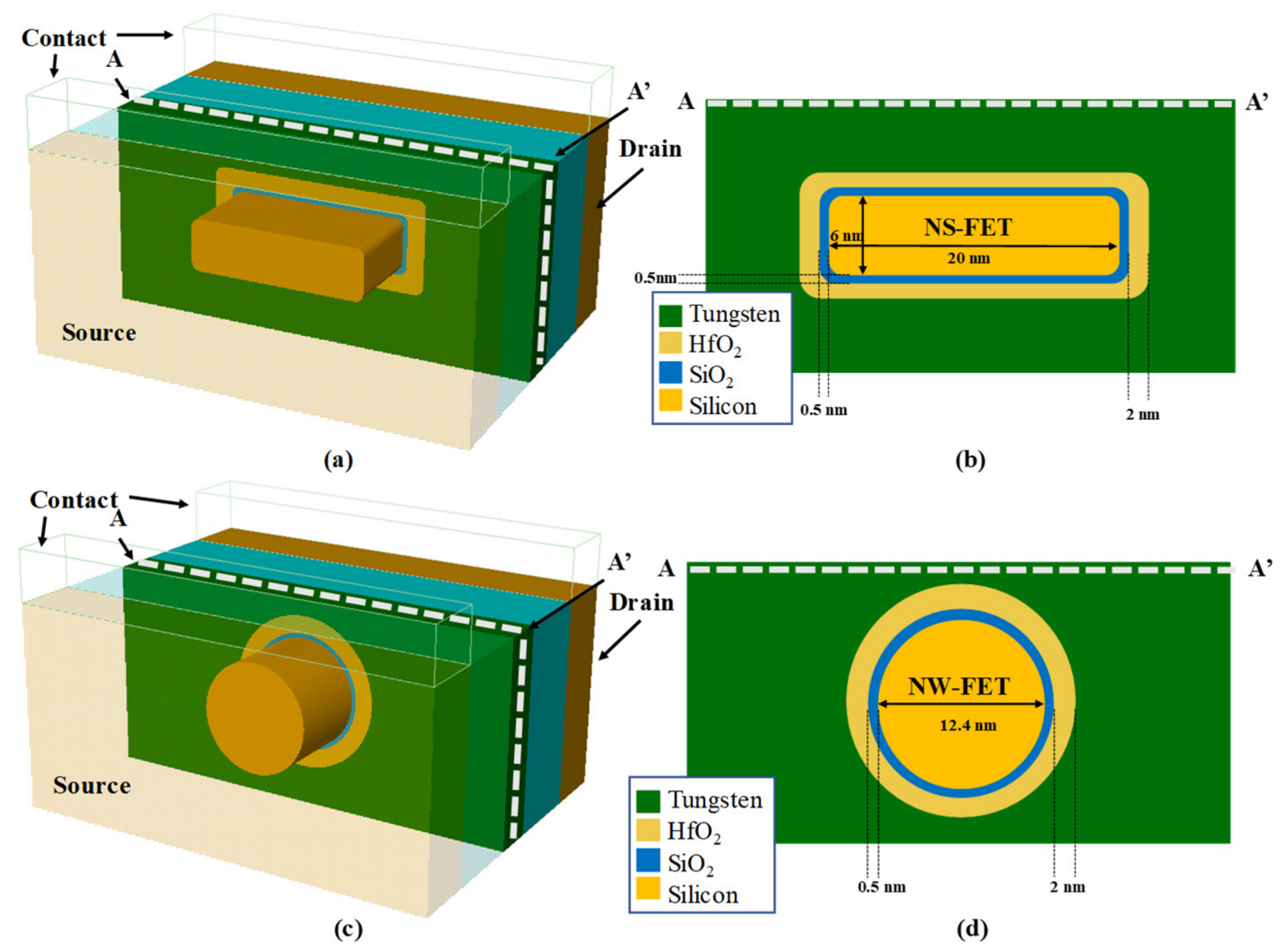
Figure 1 shows the structures designed using TCAD, and
Table 1 lists the device design parameters. For an accurate comparison, the channel cross-sectional area was designed in a similar manner. N-type doping of the device was performed using phosphorus, and p-type doping was done with boron. Silicon nitride was used as the spacer between the contacts of the device, and SiO
2 and HfO
2 were used as the gate oxides. Both devices had 0.5-nm-thick SiO
2 and 2-nm-thick HfO
2. The corner of the NS-FET channel was designed in a circular shape with a radius of 1 nm. Owing to the difference in channel shape, the NS-FET had an 8.2-nm-longer channel circumference than the NW-FET.
For the TID simulation, the Silvaco Victory device was used [
10]. In the simulation, radiation stress was applied after the gate and drain voltages were applied to the device. Among the radiation particles, γ-rays of
60Co, which causes large changes in the properties of the device because of its comparatively strong energy between other radiation particles, was used as the radiation source [
9]. Various models (trap-detrap, mobility, etc.) were used to improve the accuracy of the simulation [
11,
12,
13,
14]. After irradiation at 1 rad/s, when the desired amount of radiation stress was applied, the gate voltage was swept to 0 V again. In the study, the TCAD simulation was performed at 100 k, 1 M, 10 M, 100 M rad per each devices, respectively.
3. The Procedure of Parameter Extraction
3.1. Result of TID Effect Simulation
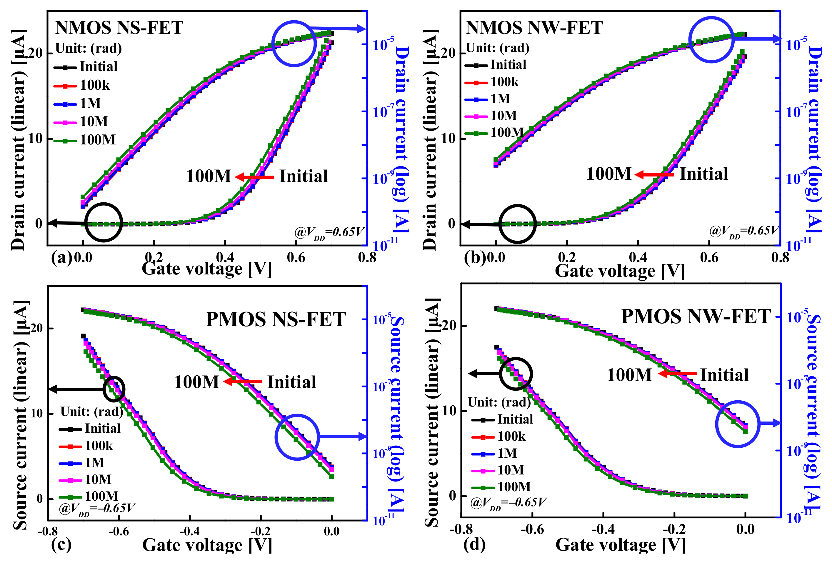
Figure 2 shows the
VT shift for each device as the total radiation dose increased. Both the NMOS and the PMOS graph shifted to the left. This is because
VT decreased in NMOS, but
VT increased in PMOS, resulting in opposite characteristic changes. In the case of NMOS, it was confirmed that
VT decreased, so the on current increased and leakage current increases. In addition, in the case of PMOS, it was confirmed that the on current and leakage current decreased as
VT increased.
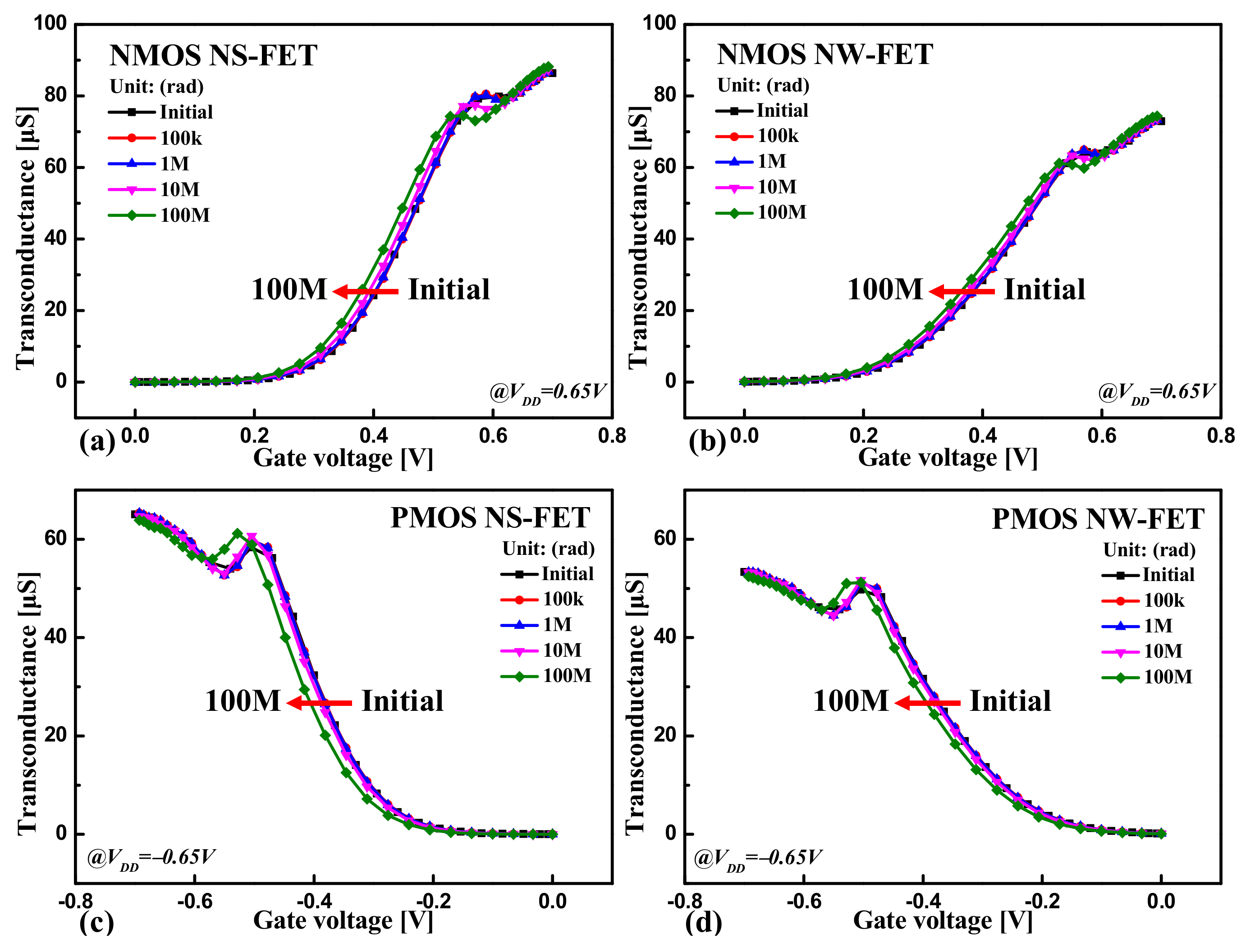
Figure 3 shows the transconductance for each device as the total radiation dose increased. In the case of NMOS, the transconductance tends to increase as the total dose of radiation increases. On the other hand, a section in which the transfer conductance is seen as a reversal of the tendency is observed at a gate voltage of 0.5 V or more, which is a phenomenon that occurs only in a section in which the transconductance decreases or the increases are temporarily delayed [
15]. It can be seen that the same phenomenon occurred in PMOS as well. In the case of PMOS, as the total radiation dose increased, the transfer conductance tended to decrease, and the period in which the inversion of the trend occurred was also confirmed.
Table 2 shows the trapped hole densities and hole trap capture rates at the SiO
2 and Si interface. In the NS-FET and NW-FET devices, interface hole traps occurred because of the TID effects. Because of the wider gate oxide of the NS-FET, more hole traps occurred than in the NW-FET. In addition, in the corner region of the NS-FET, on average, more interface hole traps were generated by approximately 30% more than in the flat region. This is because the gate controllability of the corner region of the NS-FET was weaker than that of the flat region owing to the corner effect, making it more vulnerable to TID effects.
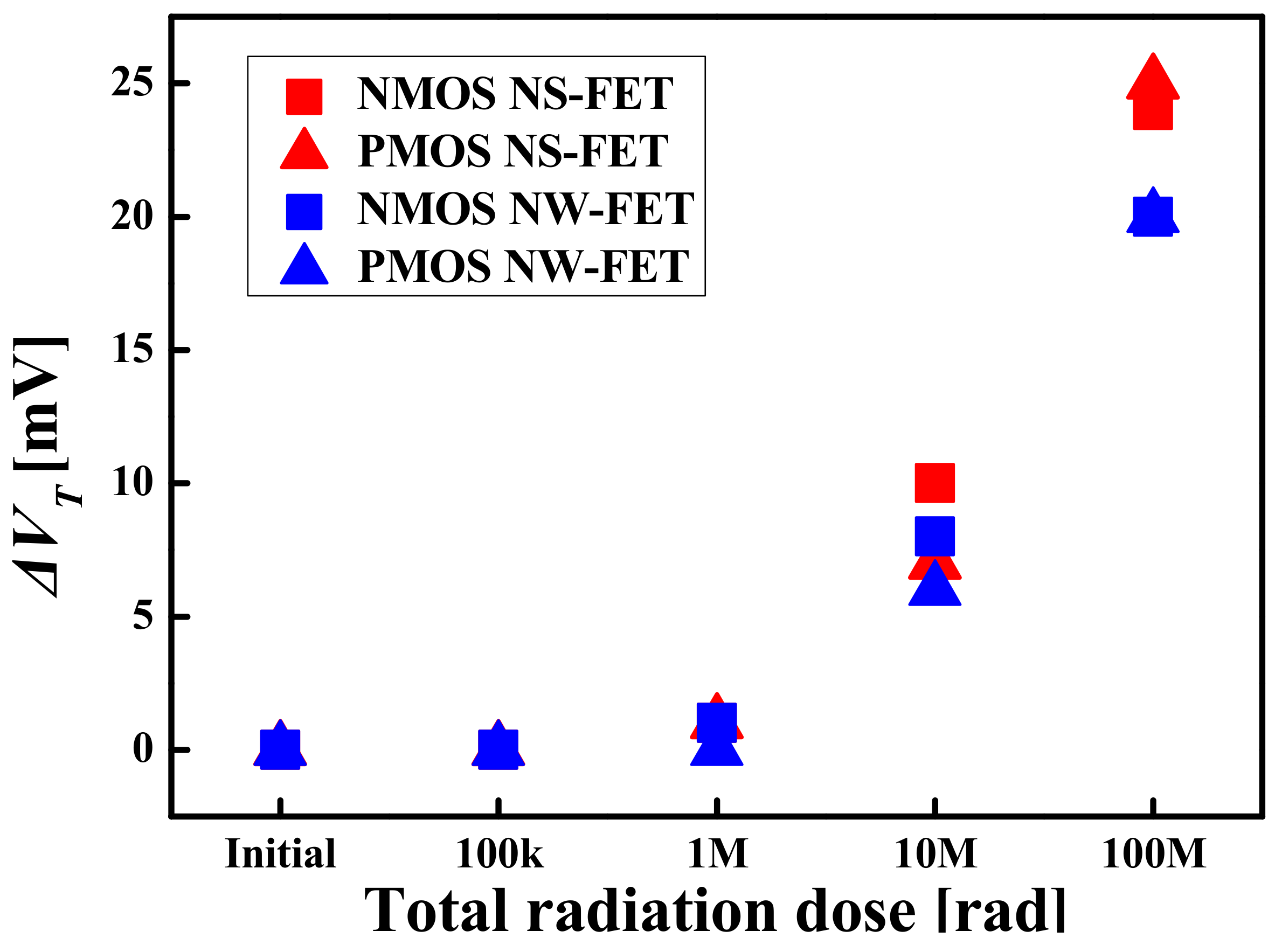
Table 3 shows
VT data of the TID simulation at each total dose rate. Although the numbers of trapped holes per unit area for the two devices are not significantly different, it was confirmed that the more
VT shift at NS-FET. This is not only affected by the total area of the oxide–the circumference of the channel also affected this. The TID effect is a phenomenon that occurs because of the hole trapped in the interface. Even if the trap is the same amount per unit area, the total amount increases in proportion to the channel circumference so that the NS-FET with a wider channel circumference eventually traps more holes.
Figure 4 shows the shifted VT according to each total dose rate. It has been already known that the VT shifts of PMOS is larger than that of NMOS in planar MOSFET because the gate length is long, and there are many places where trapping can occur in the inter-face [
16,
17]. In contrast, the GAA structure has a much shorter channel length and supe-rior gate controllability, with less variation occurring because of TID effects.
3.2. Compact Modeling Using BSIM–CMG Model Parameters
Simulation with TCAD requires an extremely long computation time, so it is difficult to immediately check the simulation results of devices that have changed characteristics (gate length, channel diameter, etc.); however, the SPICE simulation method with the extracted BSIM model parameter can obtain device characteristics faster than TCAD simulation.
The BSIM–CMG model parameters were used instead of various other commercially available BSIM model parameters to extract the device characteristics for TID effects. This is because other models, such as BSIM 4, are based on planar MOSFETs, so it is not easy to adjust a graph between simulation data values and BSIM 4 parameter values in 3D structure devices. Therefore, the BSIM–CMG model parameters were used for consistent fitting.
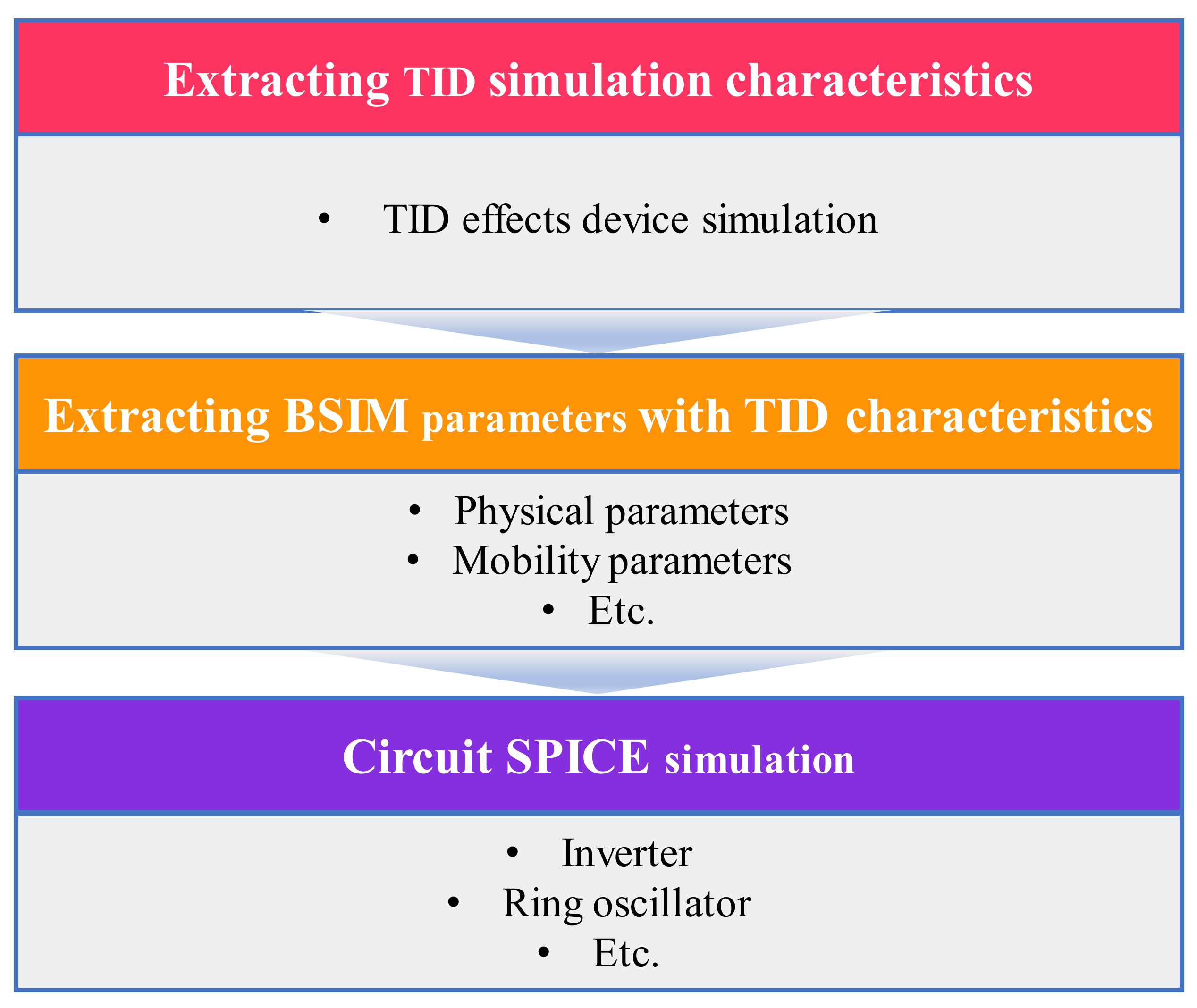
Figure 5 shows a flow chart of compact modeling considered with TID effects. First, the characteristics of the TID effect simulation data from the TCAD simulation were used for compact modeling. It is similar to an irradiation source, TCAD designs, etc. Next, the BSIM–CMG model parameters with TID effect characteristics were extracted, and the
ID–VG curve was adjusted between the TCAD simulation data and BSIM–CMG data. The extracted BSIM model parameters include the physical parameters (structure, doping, material, channel length, etc.), linear region fitting parameters (mobility, series resistance, etc.), SCE parameters (drain-induced barrier lowering parameter, gate-induced drain leakage parameter, etc.), temperature, output conductance, etc. With BSIM model parameters and adjusted data with simulation results, a SPICE circuit simulation can be initiated with a circuit netlist.
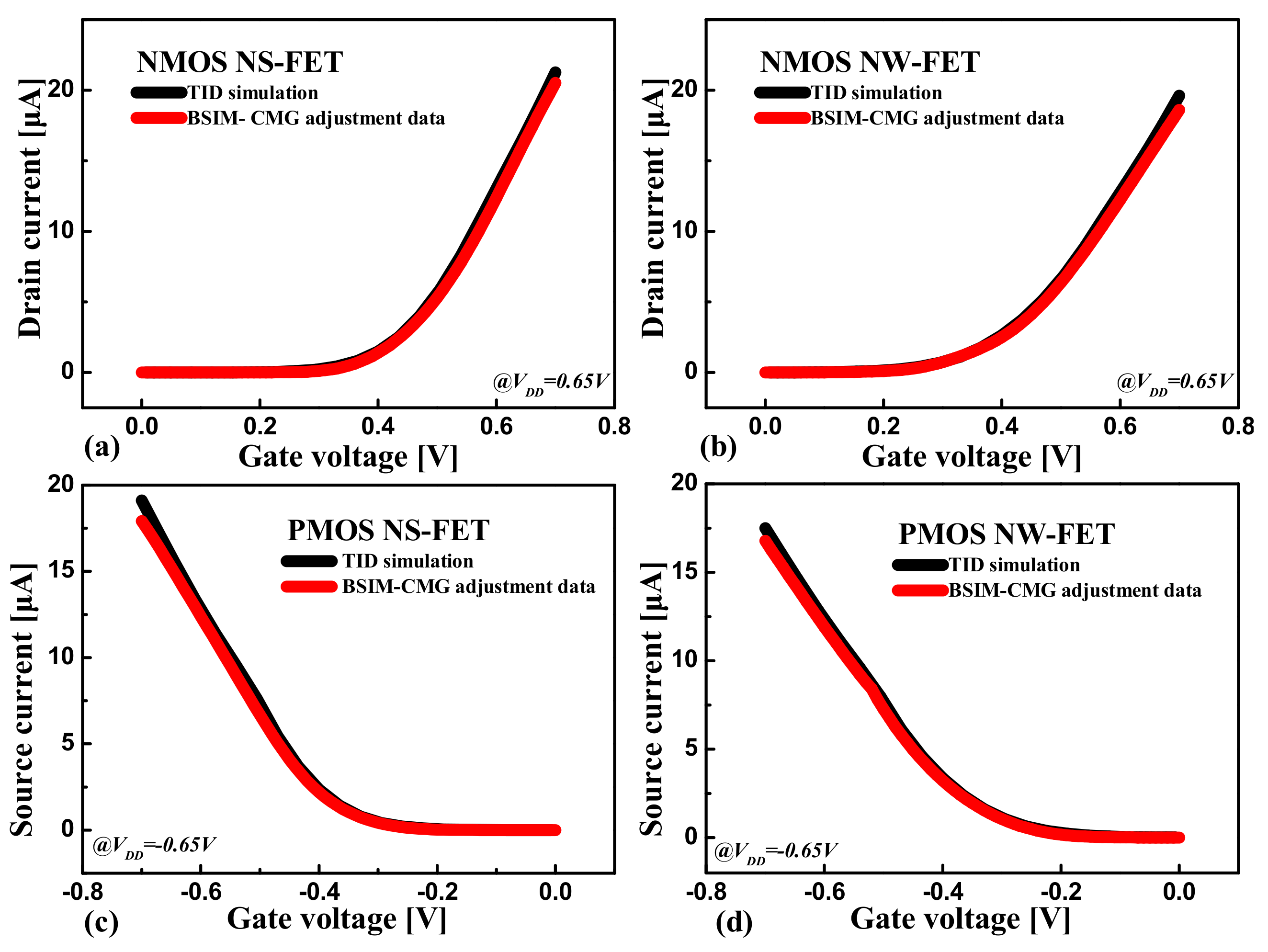
Figure 6 shows the adjusted
ID–VG curve between the TCAD simulation data and the BSIM–CMG model parameter data. All TCAD simulation data expressed in
Figure 2 were also adjusted using the BSIM–CMG model parameters. This adjustment process must be carried out carefully and consistently because consistency with the simulation data determines the reliability of the circuit simulation.
4. SPICE Circuit Simulation
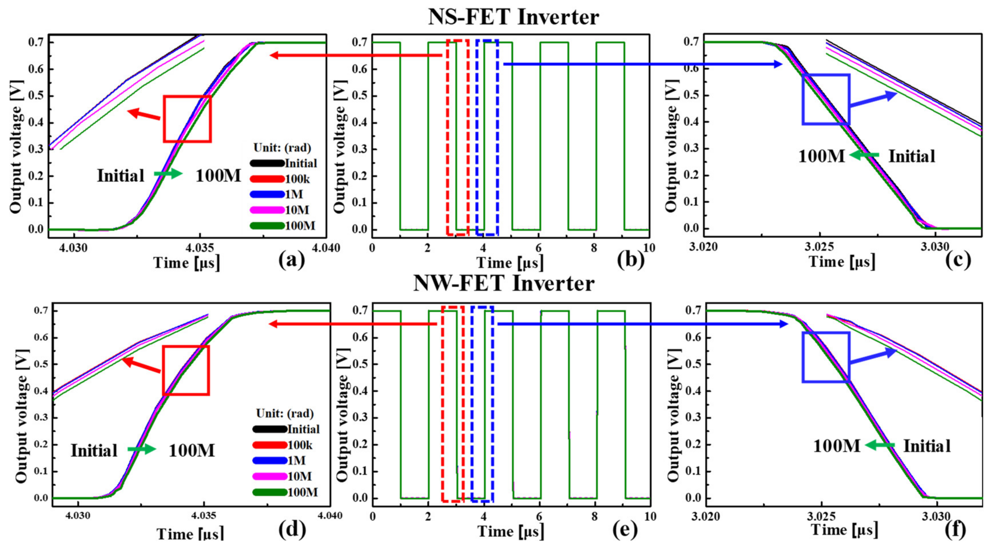
Figure 7 shows inverter operation reflecting TID effects. Because the
VT shift occurred, there was a delay in the operation of the inverter circuit [
18]. The delay of the rising edge at inverter operation was caused by the
VT shift of the PMOS so that the shifted
VT made the PMOS turn on later in order to start rising later than the nonirradiated device, and the delay of falling edge was caused by the NMOS turning off earlier than the nonirradiated device. Every rising and falling edge delay generated and accumulated after the
VT shift. The more
VT shift that occurred for the NS-FET, the more the delay generated at the NS-FET inverter.
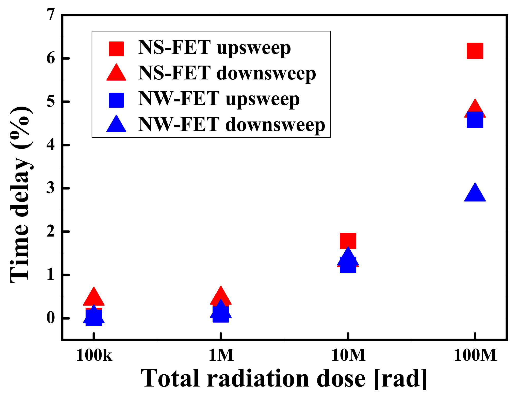
Figure 8 shows the time delay as a percentage of the inverter operation of NS-FET and NW-FET. The ratio was calculated by extracting the time delay between the device not affected by radiation and the device to be affected at output voltage 0.35 V and dividing it by 10–90% rise time (70 mV–0.63 V) of the device not affected by radiation. Both upsweep and downsweep showed that the delay of the NS-FET was more severe.
5. Conclusions
In this study, two different GAA structure devices, NS-FET and NW-FET, were designed and simulated according to the TID effects. The larger number of holes trapped in the NS-FET device was caused by the wider gate oxide area. The channel corners of the NS-FET and channel circumference differences also affected this. Owing to this structural difference, more VT shift occurred in the NS-FET than in the NW-FET.
The results indicate that it is important to reduce the total oxide area in order to have tolerance of TID effects in the GAA structure, but it is more important to design a device that can reduce the channel circumference or corner effect.
In addition, the BSIM–CMG model parameters were extracted to simulate the inverter circuit with device operation characteristics according to the TID effects. The NS-FET inverter operation had more delay variation than that of the NW-FET inverter because the NW-FET had better tolerance of TID effects, under these assumptions and structural differences, that can reduce VT shift variation.
Author Contributions
Investigation, J.L.; data curation, J.L.; visualization, J.L.; software, J.L.; validation, J.L.; formal analysis, J.L.; writing, J.L.; supervision, M.K.; project administration, M.K.; funding acquisition, M.K. All authors have read and agreed to the published version of the manuscript.
Funding
This research was funded by the National R&D Program through the National Research Foundation of Korea (NRF) funded by Ministry of Science and ICT (2021M3F3A2A03017693), and in part by the Basic Science Research Program through the National Research Foundation of Korea (NRF) funded by the Ministry of Education (2018R1A6A1A03023788).
Acknowledgments
The authors would like to thank Hyeonjae Won for his technical support.
Conflicts of Interest
The authors declare no conflict of interest.
References
- Bogaerts, J.; Dierickx, B.; Meynants, G.; Uwaerts, D. Total dose and displacement damage effects in a radiation-hardened CMOS APS. IEEE Trans. Electron. Devices 2003, 50, 84–90. [Google Scholar] [CrossRef]
- Nichols, D.K.; McCarty, K.P.; Coss, J.R.; Waskiewicz, A.; Groninger, J.; Oberg, D.; Koga, R. Observations of single event failure in power MOSFETs. In Proceedings of the IEEE Radiation Effects Data Workshop, Tucson, AZ, USA, 20 July 1994; pp. 41–54. [Google Scholar]
- Jeong, K.; Ro, D.; Lee, G.; Kang, M.; Lee, H.M. A radiation-hardened instrumentation amplifier for sensor readout integrated circuits in nuclear fusion applications. Electronics 2018, 7, 429. [Google Scholar] [CrossRef] [Green Version]
- Ferlet-Cavrois, V.; Massengill, L.W.; Gouker, P. Single event transients in digital CMOS—A review. IEEE Trans. Nucl. Sci. 2013, 60, 1767–1790. [Google Scholar] [CrossRef]
- Barnaby, H.J. Total-ionizing-dose effects in modern CMOS technologies. IEEE Trans. Nucl. Sci. 2006, 53, 3103–3121. [Google Scholar] [CrossRef]
- Seo, D.; Han, J.W.; Kim, J.; Lee, S.; Chang, I.J. Total Ionizing Dose Effect on Ring Oscillator Frequency in 28-nm FD-SOI Technology. IEEE Electron. Device Lett. 2018, 39, 1728–1731. [Google Scholar] [CrossRef]
- Guerfi, Y.; Larrieu, G. Vertical silicon nanowire field effect transistors with nanoscale gate-all-around. Nanoscale Res. Lett. 2016, 11, 1–7. [Google Scholar] [CrossRef] [PubMed] [Green Version]
- Wu, C.C.; Lin, D.W.; Keshavarzi, A.; Huang, C.H.; Chan, C.T.; Tseng, C.H.; Mii, Y.J. High performance 22/20nm FinFET CMOS devices with advanced high-K/metal gate scheme. In Proceedings of the International Electron. Devices Meeting, San Francisco, CA, USA, 6–8 December 2010; p. 27. [Google Scholar]
- Oldham, T.R.; McLean, F.B. Total ionizing dose effects in MOS oxides and devices. IEEE Trans. Nucl. Sci. 2003, 50, 483–499. [Google Scholar] [CrossRef] [Green Version]
- Silvaco Victory Device User’s Manual. Available online: https://www.silvaco.com/products/tcad/device_simulation/victory_device/victory_device.html (accessed on 26 January 2015).
- Won, H.; Ham, I.; Jeong, Y.; Kang, M. Comparison of Various Factors Affected TID Tolerance in FinFET and Nanowire FET. Appl. Sci. 2019, 9, 3163. [Google Scholar] [CrossRef] [Green Version]
- Hurkx, G.A.M.; Klaassen, D.B.M.; Knuvers, M.P.G. A new recombination model for device simulation including tunneling. IEEE Trans. Electron. Devices 1992, 39, 331–338. [Google Scholar] [CrossRef]
- Kimpton, D.; Kerr, J. A simple trap-detrap model for accurate prediction of radiation induced threshold voltage shifts in radiation tolerant oxides for all static or time variant oxide fields. Solid State Electron. 1994, 37, 153–158. [Google Scholar] [CrossRef]
- Hastas, N.A.; Dimitriadis, C.A.; Brini, J.; Kamarinos, G.; Gueorguiev, V.K.; Kaschieva, S. Effects of gamma-ray irradiation on polycrystalline silicon thin-film transistors. Microelectron. Reliab. 2003, 43, 57–60. [Google Scholar] [CrossRef]
- Huang, Y.; Li, B.; Zhao, X.; Zheng, Z.; Gao, J.; Zhang, G.; Li, B.; Zhang, G.; Tang, K.; Han, Z. An effective method to compensate total ionizing dose-induced degradation on double-SOI structure. IEEE Trans. Nucl. Sci. 2018, 65, 1532–1539. [Google Scholar] [CrossRef]
- Gaillardin, M.; Marcandella, C.; Martinez, M.; Duhamel, O.; Lagutere, T.; Paillet, P.; Vinet, M. Total ionizing dose response of multiple-gate nanowire field effect transistors. IEEE Trans. Nucl. Sci. 2017, 64, 2061–2068. [Google Scholar] [CrossRef]
- Won, H.; Kang, M. Analysis of Circuit Simulation Considering Total Ionizing Dose Effects on FinFET and Nanowire FET. Appl. Sci. 2021, 11, 894. [Google Scholar] [CrossRef]
- Clark, L.T.; Pettit, D.E.; Holbert, K.E.; Hindman, N.D. Validation of and delay variation in total ionizing dose hardened standard cell libraries. In Proceedings of the IEEE International Symposium of Circuits and Systems, Rio de Janeiro, Brazil, 15–18 May 2011; pp. 2051–2054. [Google Scholar]
| Publisher’s Note: MDPI stays neutral with regard to jurisdictional claims in published maps and institutional affiliations. |
© 2021 by the authors. Licensee MDPI, Basel, Switzerland. This article is an open access article distributed under the terms and conditions of the Creative Commons Attribution (CC BY) license (https://creativecommons.org/licenses/by/4.0/).


