Article

Sheet Resistance Measurements of Conductive Thin Films: A Comparison of Techniques

1
National Physical Laboratory, Teddington TW11 0LW, UK
2
PragmatIC Semiconductor Limited, Cambridge CB4 0WH, UK
*
Author to whom correspondence should be addressed.
Electronics 2021, 10(8), 960; https://doi.org/10.3390/electronics10080960
Submission received: 29 March 2021 / Revised: 13 April 2021 / Accepted: 14 April 2021 / Published: 17 April 2021
(This article belongs to the Section Microelectronics)

Abstract

:
Conductive thin films are an essential component of many electronic devices. Measuring their conductivity accurately is necessary for quality control and process monitoring. We compare conductivity measurements on films for flexible electronics using three different techniques: four-point probe, microwave resonator and terahertz time-domain spectroscopy. Multiple samples were examined, facilitating the comparison of the three techniques. Sheet resistance values at DC, microwave and terahertz frequencies were obtained and were found to be in close agreement.

1. Introduction

Transparent thin conductive films were first discovered at the beginning of the 20th century and have since become a major area of the electronics industry, with a wide variety of applications, including touch screens, flat panel displays and solar cells. In recent years, a new area of application of flexible electronics has attracted much interest and development effort, requiring new types of thin films. The technology, properties and physics of thin conducting films have been reviewed in several papers [1,2,3,4], and a survey of the field has appeared as a handbook [5].
In semiconductor fabrication, various processing steps directly impact the electrical properties of thin films. Non-destructive, fast, accurate measurements, sensitive to changes in thin-film electrical properties are required to monitor thin films during fabrication, enabling in-line process control, optimisation and early identification of process excursions. Metal oxide thin films of a few nanometres to a few tens of nanometres thickness are extensively used in applications and are sensitive to a range of processes performed on the metal oxide films themselves, as well as processes performed on underlying and overlying films.
Sheet resistance (Rs), a critical electrical property, is used to characterise films of semiconducting and conducting materials. It is a measure of lateral resistance per square area of a film with uniform thickness, and quantifies the ability of electrical charge to travel in the plane of the film. The standard technique for measuring sheet resistance is the four-point probe; however, it requires physical contact with the film and is relatively slow. It is therefore unsuited for in-line process control on a production line.
In this paper, we investigate the use of two non-contact techniques for measuring sheet resistance, both of which are capable of near-real-time measurement over large areas: microwave resonator (MW) and terahertz time-domain spectroscopy (THz TDS). These are compared with the four-point probe method, which is the standard technique for measuring sheet resistance. We describe the measurement processes and data analysis and present a comparison of measurement results obtained by the three techniques on a set of thin films manufactured for the study. To our knowledge, this is the first study where these three measurement techniques are applied to the same set of samples, evaluating technique performance and providing a direct comparison of measured sheet resistance at DC, microwave and terahertz frequencies.

2. Materials and Methods

2.1. Sample Preparation/Configuration

In order to enable comparison of the four-point probe, Microwave resonator (MW) and Terahertz time-domain spectroscopy (THz TDS) measurement techniques, a total of 12 Indium Gallium Zinc Oxide (IGZO) films were deposited onto PragmatIC’s substrates (200 mm diameter Borofloat glass wafers pre-coated with polyimide and an insulating layer). The 12 samples were subjected to a range of post-deposition treatments in order to provide samples of differing sheet resistances. To support the different measurement techniques used in this work, a thin layer of titanium (Ti) was deposited on top of the IGZO films.

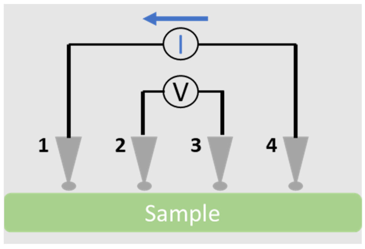
2.2. Four-Point Probe

The “four-point probe” (4pp) method is the most common and simplest technique for measuring the sheet resistance (Rs) of thin films [6,7,8,9]. A typical four-point probe tool (shown in Figure 1 below) has four equally spaced, co-linear probes which are used to make electrical contact with the material to be characterised. To calculate the Rs, a DC current is applied through the outer probes which induces a voltage across the two inner probes. By measuring this voltage drop, the sheet resistance can be calculated using Equation (1) [6,7]:
R S = π l n ( 2 )   Δ V I = 4.53236   Δ V I
where Rs is the sheet resistance (expressed in Ω/sq.), ΔV is the voltage drop measured across the inner probes and I is the current applied at the outer probes.
In addition to the factor π/ln(2) in Equation (1) above, a geometric correction factor is required, which accounts for the limitation of current pathways through the sample, and this factor is based on the sample size, shape and thickness and the position of the probes [8,9].
If the thickness of the material being measured is known, the sheet resistance can be used to calculate its resistivity by using Equation (2) [6,7]:
R S = ρ t f
where, ρ is the resistivity and tf is the film thickness.
A Keithley source measurement unit (SMU) 2612A together with the four-point probe setup was used to measure the sheet resistance of all the samples. After the sample was placed in the holder and the probes were put in contact with the film, the target current was applied via the SMU and the voltage drop was subsequently measured. To study the sheet resistance variation across the films, a full wafer mapping was carried out across the full extent of the 200 mm wafers, with a total of 20 points per wafer measured; the mean and standard deviation were calculated and are reported below.
Sheet resistance was seen to vary significantly and irregularly over the area of each wafer, as discussed below. Therefore, in order to enable accurate comparison between the three measurement techniques, it was necessary to define precisely the measurement locations on wafers. For that purpose, after the initial analysis, the 12 wafers were diced, (size 2 cm × 2 cm) targeting different areas of the wafers: centre, top, bottom, left and right. For these diced samples, measurements were carried out on the centre with a total of four measurement points per sample; the mean and standard deviation were calculated and are reported below.

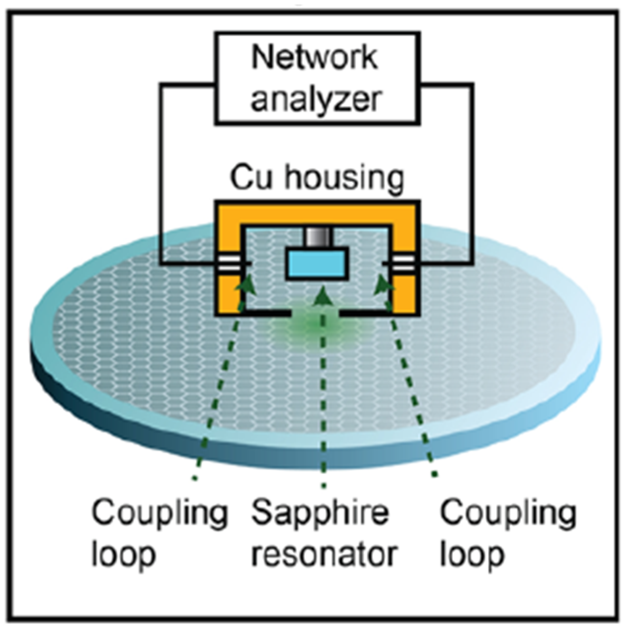
2.3. Microwave Resonator

Non-contact measurement methods are particularly attractive when the film to be measured is either very thin, fragile or buried beneath an insulating layer. The perturbation of a high-quality factor (Q) dielectric microwave resonator was first developed as a means of characterising superconducting thin films [10,11] and more recently it has been developed to look at graphene thin films, down to 0.4 nm thickness, without the need for contacts [12]. This method is suitable for small samples (<10 mm in scale) which can be fitted within the housing of the dielectric resonator, close enough that the thin film and its substrate perturb the fringing field of the resonator. For larger samples or for scanned techniques we have developed a method in which the film to be measured is situated outside the resonator which has an aperture through which the fringing field extends into the region of the film. Figure 2 shows a schematic of the dielectric resonator set-up for the thin film sheet resistance measurement.
Using this open resonator technique, a larger sample may be scanned over the aperture and values of sheet resistance plotted as a function of the position of the aperture in relation to the film [13].
Recently, at the National Physical Laboratory, we developed an automated wafer scanning instrument in which a wafer up to 200 mm in diameter can be scanned across the resonator aperture, and at each scan point, a sheet resistance value is acquired by software. In this prototype microwave scanner, the wafer is translated below the resonator aperture, in two orthogonal directions using two stepper motors driving lead screws. The measurement process involves accurate measurement of centre frequency and linewidth of a microwave resonance (TE01 mode). By combining these with equivalent measurements on an uncoated but otherwise identical wafer, the sheet resistance Rs can be determined [14].
R s = Δ f s π   f 0   ε 0   ( Δ w g Δ w s )   ( ε s 1 )   t s
In Equation (3), Δfs is the frequency shift between the coated wafer and the bare substrate resonances, ΔwcΔws is the difference in the resonance linewidth between the coated and bare wafers, f0 is the centre frequency, ε0 is the permittivity of free space and ε’s is the real part of the permittivity of the bare substrate which has thickness ts.
To measure the sheet resistance across a whole wafer, the wafer is centred with the coated film uppermost on the polystyrene wafer table. The resonator vertical position is adjusted to bring the open aperture within around 3–5 mm of the wafer surface, and the laser distance sensor is activated. Then the step size in both x and y directions is set (typically in the range of 5–20 mm, depending on the aperture size). The wafer is positioned at the start of the scan and a sequence of measurements of Rs is made at each position as the scan proceeds across a raster pattern covering the entire extent of the wafer. A display indicates the variation of Rs with the scan position, while the data for centre frequency, linewidth and vertical position are recorded to a data file. At the end of the scan, the wafer is returned to the home position to allow it to be easily removed from the table. The measurement frequency is 3.25 GHz.

2.4. Terahertz Time-Domain Spectroscopy

Techniques for using terahertz time-domain spectroscopy (THz TDS) for the measurements of thin-film sheet resistance are well known and have been employed for a variety of conductive films, such as gold [15], ITO [16,17], graphene [18,19] and flexible electronics [20].
Sheet resistance at THz frequencies can be determined by measuring THz transmission through the test film, and is calculated from [20]:
R s = Z 0 / [ ( 1 + n s ) t ( 1 + n s ) ]
where Rs is sheet resistance, t is amplitude transmission, ns is the THz refractive index of the substrate material and Z0 = 376.7 Ω is the vacuum impedance. The amplitude transmission t is determined by measuring the THz field amplitude transmitted through a bare substrate (Esub) and through the coated test wafer (Ew) and calculating their ratio: t = Ew/Esub.
There are two possible approaches for implementing such measurements in THz TDS. Figure 3 shows the method for obtaining frequency-averaged sheet resistance, which can be derived directly from the time-domain data. In this case, t is calculated as the ratio of peak-to-peak amplitudes of the main pulse. The advantage of this method is that it is fast and requires minimal data processing.
The second approach, depicted in Figure 4, yields frequency-resolved sheet resistance and requires Fourier transforms to be applied to the time-domain data. Here, transmission t is calculated as the ratio of spectral amplitudes. The advantage of this method is that it provides information on the frequency behaviour of sheet resistance.
Both frequency-averaged and frequency-resolved methods were used in our study. Frequency-resolved measurements confirmed that wafer sheet resistance had a low frequency dispersion (see below), allowing the frequency-averaged approach to be used for most measurements.
The application of Equation (4) requires knowledge of the refractive index of the substrate material. In our study, it was measured using THz TDS and is shown in Figure 5. A value of 2.1 was employed in frequency-averaged measurements since >96% of beam power is carried at frequencies below 1.5 THz. A frequency-dependent refractive index was used for calculating frequency-resolved sheet resistance.
To show the relationship between transmission and sheet resistance according to Equation (4), Figure 6 plots the dependence of sheet resistance on transmission (assuming ns = 2.1).
THz TDS measurements were performed using a Toptica TeraFlash spectrometer. The THz beam path configuration was a standard four-parabolic setup, with sample positions in the collimated beam and at the beam focus. The diameter of the collimated beam was 25 mm, and the diameter of the focused beam (full width at half maximum) was 2 mm. A standard PragmatIC substrate without the IGZO layer was used as a reference in transmission measurements.
Since the variation of sheet resistance across the wafer was of particular interest in this study, all measurements were carried out with the samples placed in the focal plane of the THz beam. There was no facility available for raster scanning. Sheet resistance at different locations on whole wafers was measured by rotating the wafers. The wafer was placed so that the THz beam traversed it 25 mm from the edge. It was then rotated in steps of approximately 30°, producing a series of measurements around the rim. The location above the notch in the wafer edge was designated as 0°. A total of 25 measurements were taken of each wafer, that is, twice around the circumference. This allowed reproducibility to be confirmed.
All wafers had one randomly chosen location measured by using a time-domain sweep and analysing the data to obtain frequency-resolved sheet resistance; these were done by placing the wafer in the collimated beam to increase accuracy. However, the great majority of measurements were carried out using peak-to-peak amplitudes of the main time-domain pulse, producing frequency-averaged sheet resistance. All diced samples were measured only by the peak-to-peak method.
The measurement uncertainty was evaluated as the standard deviation of repeated measurements and was found to be <0.5%.

3. Results and Discussion

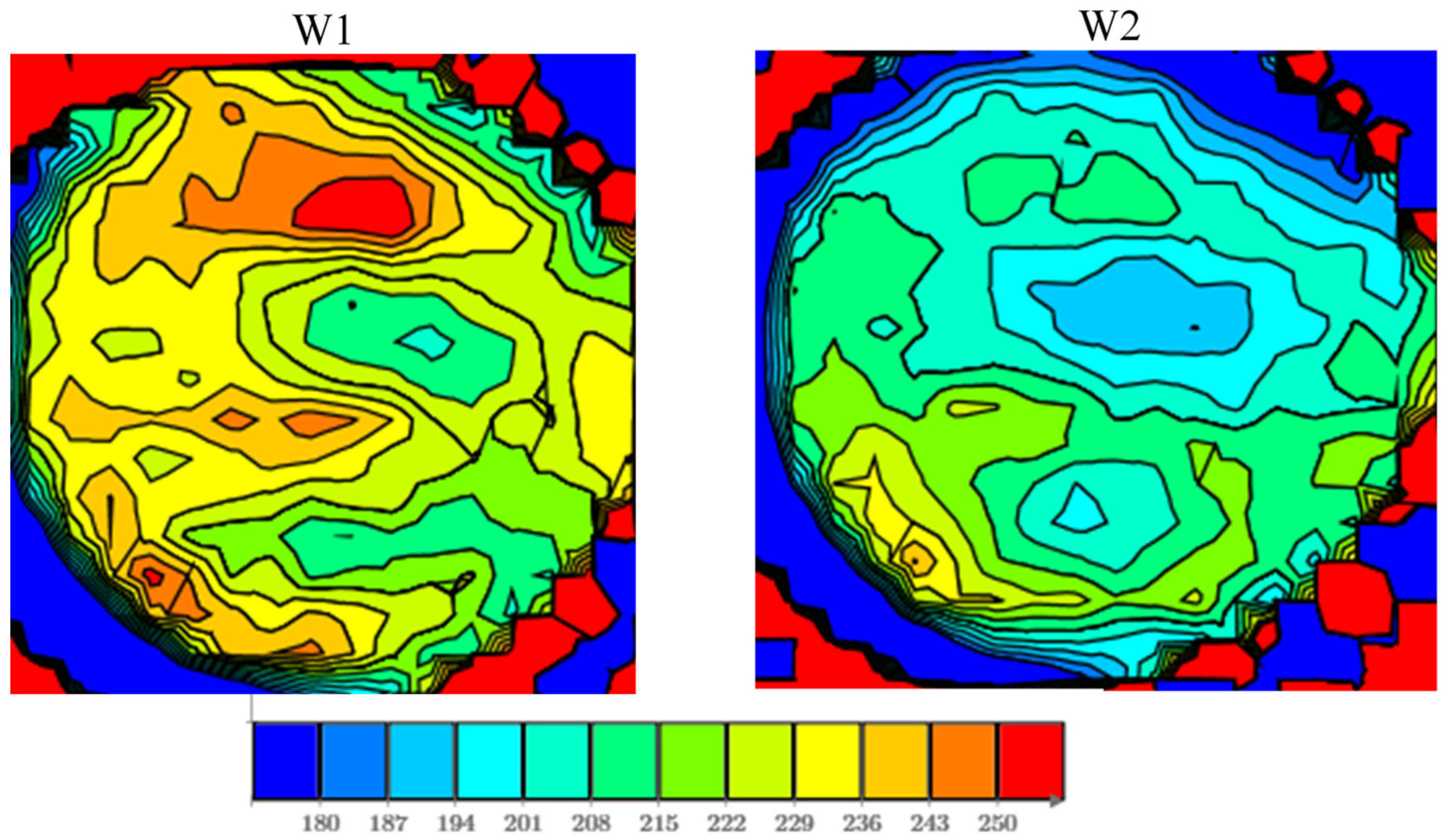
3.1. Microwave Resonator

Figure 7 shows representative maps of the sheet resistance of two wafers (200 mm diameter). The contour lines are separated by ~3.5% of the mean sheet resistance. The mean values and standard deviations of the measurements for these two wafers are given in the figure caption.
It is seen that sheet resistance varies by as much as 20% over the area of the wafer and that the variation pattern is irregular. It is therefore not possible to extrapolate sheet resistance from a few measurement locations. Hence, a full and detailed resistance image of a wafer is required, such as that shown in Figure 7.
The mean value of sheet resistance over the wafer area and its standard deviation for all wafers are reported in Figure 10 below. In the case of diced samples, each sample was measured four times, and the mean and standard deviation are reported in Figure 11 below.

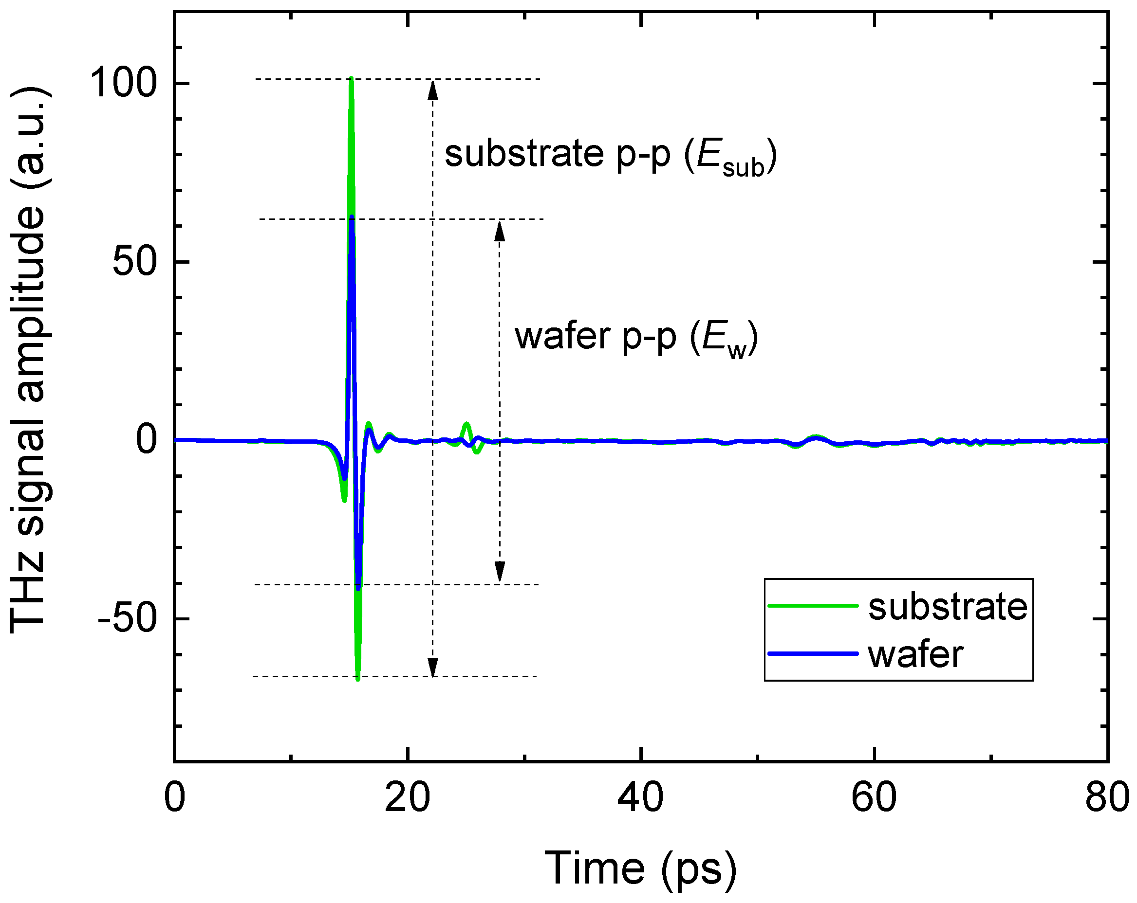
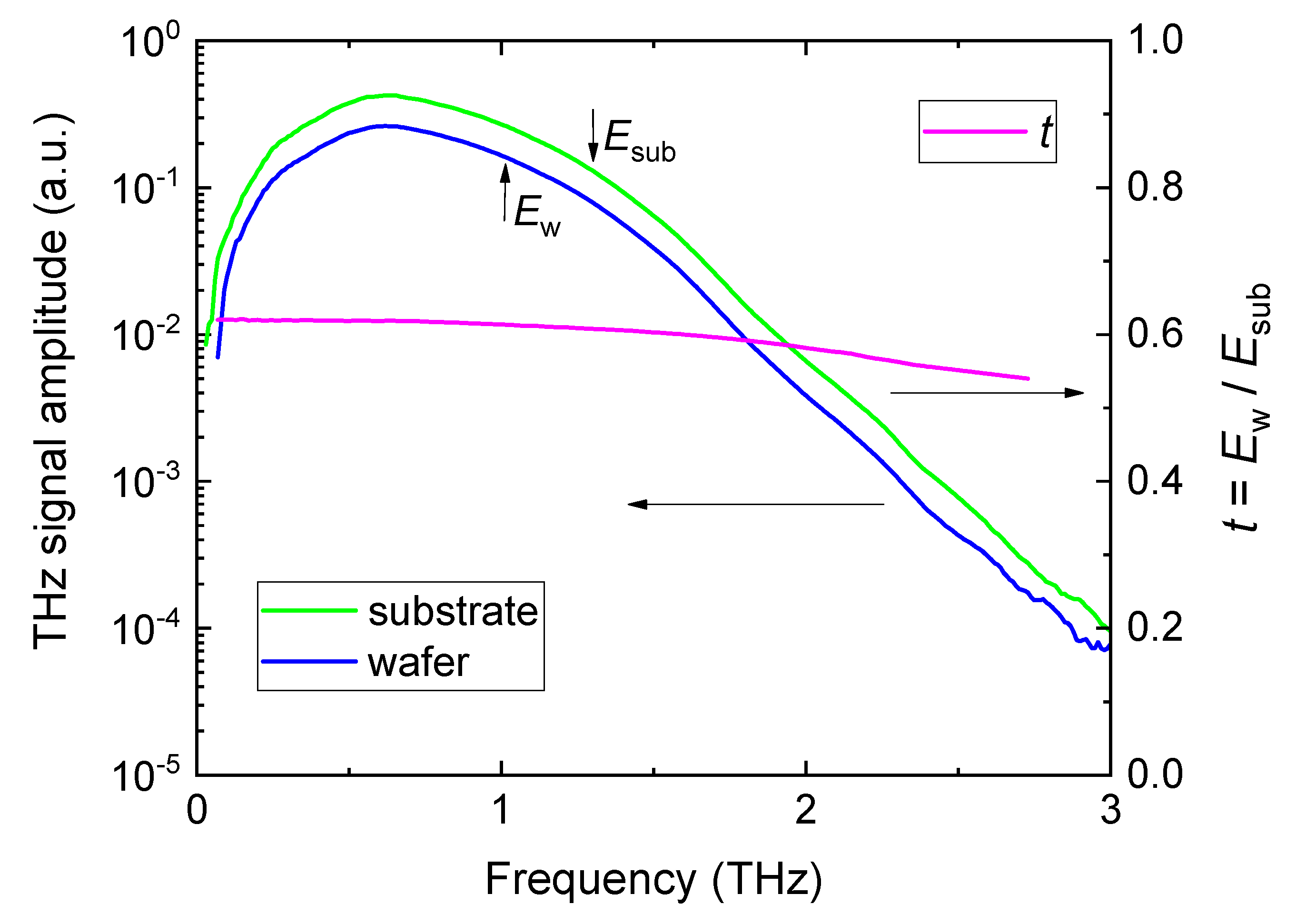
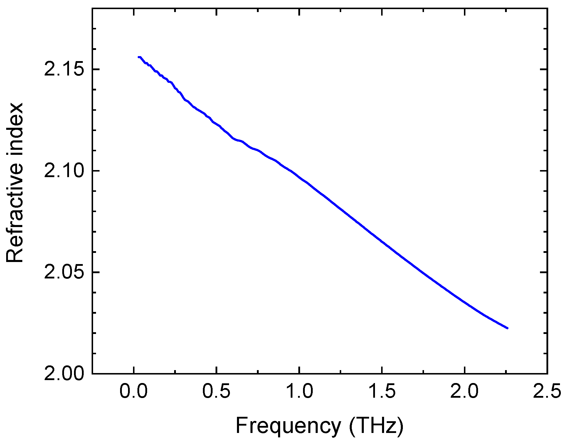
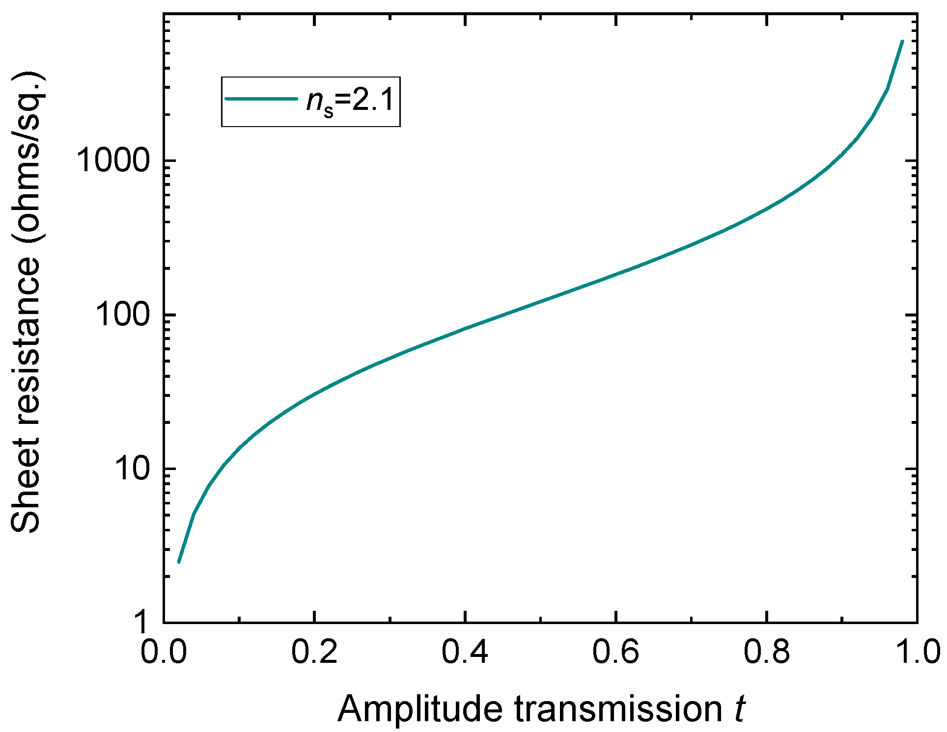
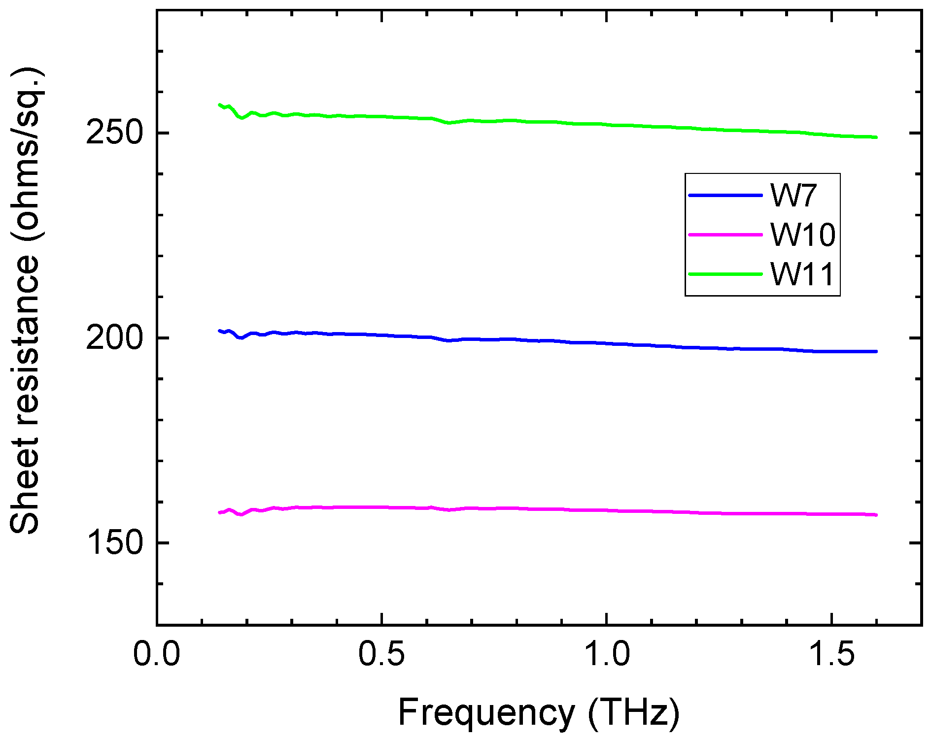
3.2. Terahertz TIME-Domain Spectroscopy

Figure 8 shows three examples of frequency-resolved sheet resistance, measured in wafers with low, medium and high sheet resistance. Frequency dispersion is seen to be <10%, which justifies using frequency-averaged measurements.
Figure 9 presents three examples of variation in sheet resistance measured around the circumference of wafers 25 mm from the edge. As with MW measurements, sheet resistance is seen to vary by up to 20%, in an irregular pattern that is different in every wafer. Notably, in most wafers examined, the difference between minimum and maximum sheet resistance values is larger where the mean sheet resistance is higher.
The mean value of sheet resistance over the wafer circumference and its standard deviation for all wafers are reported in Figure 10 below. In the case of diced samples, each sample was measured four times, and the mean and standard deviation are reported in Figure 11 below.

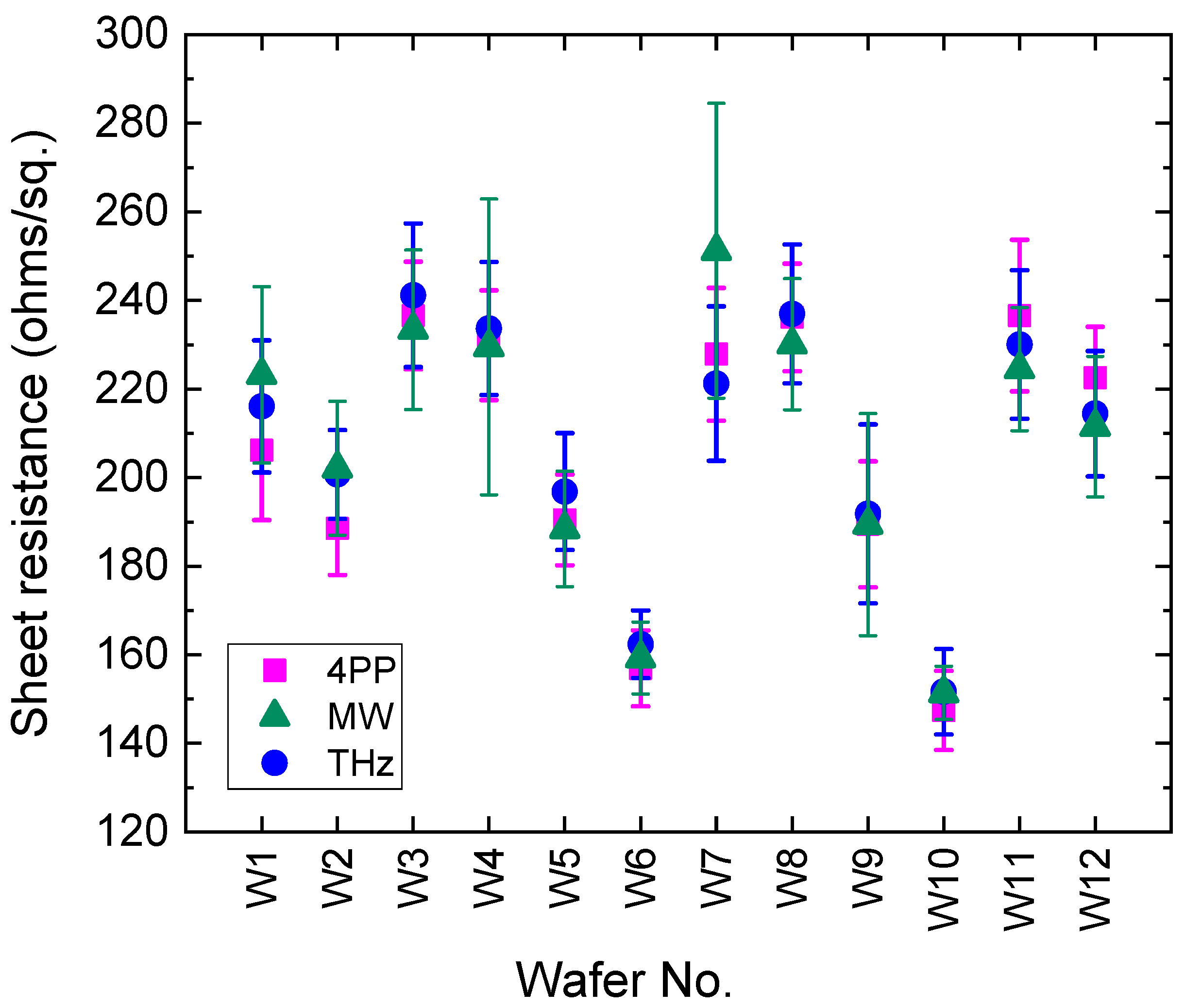
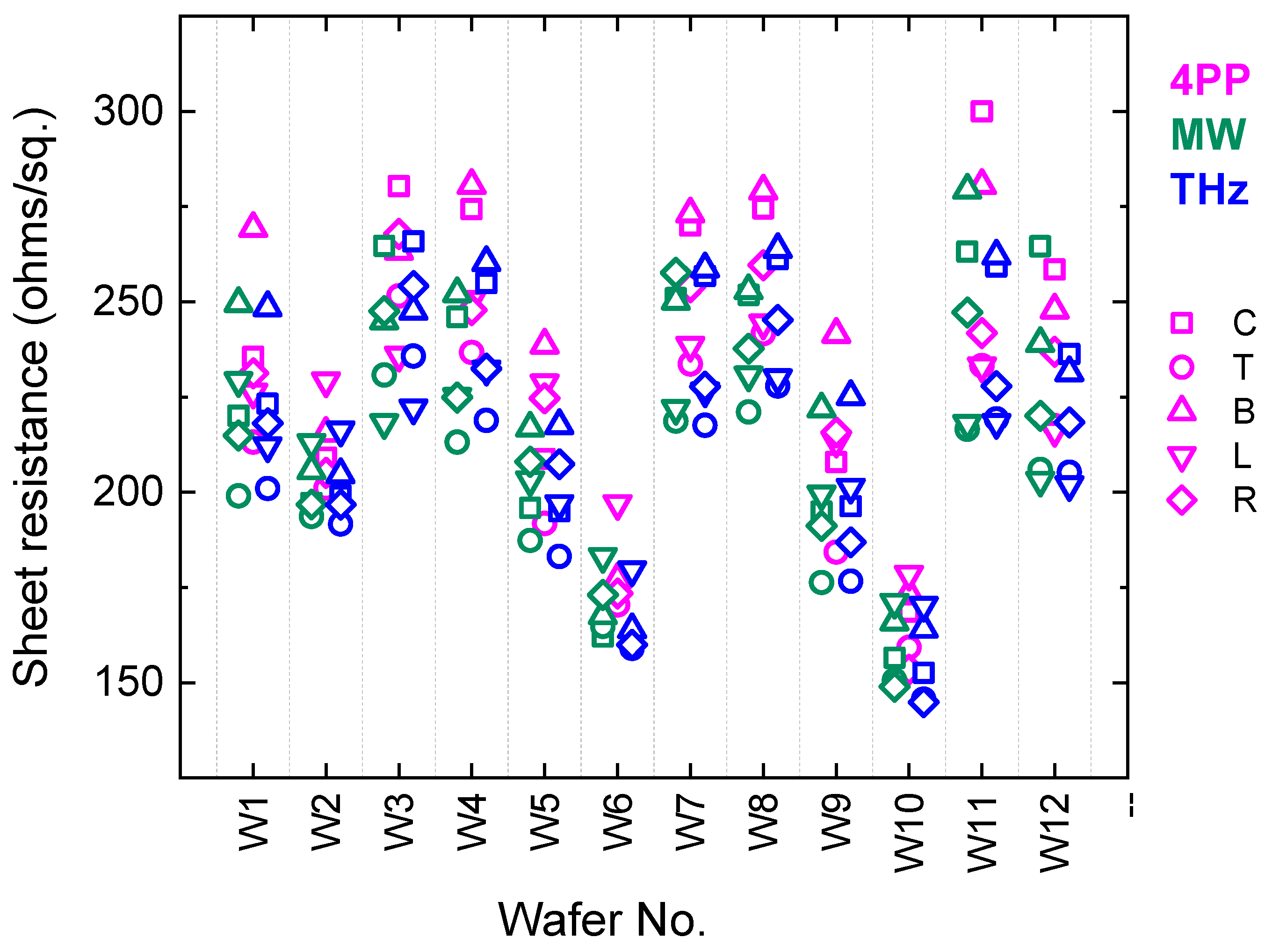
3.3. Comparison of Sheet Resistance Measurement Results

The measured sheet resistance is determined primarily by the properties of the top Ti layer that has been influenced by the various IGZO post-deposition processing conditions. Figure 10 shows the mean and standard deviation of all measurements on each of the 12 wafers using the three measurement techniques (four-point probe, MW resonator, THz TDS). Good agreement is evident between the three measurement techniques.
However, it must be noted that the number of measurements per wafer and their locations were different for each measurement technique. As seen in Figure 7 and Figure 9, the sheet resistance of a wafer varies significantly and irregularly over its area. Therefore, selecting different measurement locations may affect the mean sheet resistance observed and its standard deviation.
In order to obtain an accurate comparison between the three measurement techniques, the measurement area had to be precisely defined. This was achieved by dicing the wafers into 20 mm × 20 mm sections, as explained above in Section 2.2. Although the aim of the study was to compare non-destructive measurement techniques capable of providing full-area images, dicing the wafers was undertaken as a necessary step in measurement comparison. The obtained sheet resistance values are depicted in Figure 11, where sheet resistance values at five locations on each wafer are plotted as measured by the three techniques. As in Figure 10, the results in Figure 11 show good agreement.

4. Conclusions

We studied sheet resistance of thin conducting film on 200 mm glass substrates, aiming to demonstrate a non-contact rapid measurement technique suitable for in-line process control of wafer manufacturing. Two non-contact techniques were employed and evaluated: microwave resonator and THz time-domain spectroscopy. The results were also compared with those obtained by the four-point probe method, which is the standard method for sheet resistance measurements.
Numerous samples were measured, providing sheet resistance values at DC, microwave and terahertz frequencies. In all samples studied, the sheet resistance values obtained by the three techniques were found to be in close agreement, showing that film conductivity remains constant over the range of frequencies from DC to THz.
Both microwave resonator and terahertz time-domain spectroscopy were demonstrated to be suitable for the purpose of in-line process control of conductive thin films.

Author Contributions

Conceptualization, M.N., L.H., S.D., F.A.; methodology, M.N., J.G., S.D., F.A.; software, K.P.; validation, M.N., S.D.; formal analysis, M.N., J.G., S.D., F.A.; investigation, M.N., J.G., L.H., K.P., S.D., F.A.; resources, L.H., F.A., C.R.; data curation, K.P.; writing—original draft preparation, M.N., J.G., S.D., F.A., C.R.; writing—review and editing, M.N., S.D., F.A., C.R.; visualization, M.N.; supervision, L.H.; project administration, D.K., S.C.; funding acquisition, F.A., C.R., D.K. All authors have read and agreed to the published version of the manuscript.

Funding

This research was funded by Innovate UK under the A4I programme, Project 105554 “MASCOT” and by the National Measurement System Programmes Unit of the UK Department for Business, Innovation and Skills.

Conflicts of Interest

The authors declare no conflict of interest.

References

  1. Ellmer, K. Past achievements and future challenges in the development of optically transparent electrodes. Nat. Photonics 2012, 6, 809–817. [Google Scholar] [CrossRef]
  2. Cao, W.; Li, J.; Chen, H.; Xue, J. Transparent electrodes for organic optoelectronic devices: A review. J. Photonics Energy 2014, 4, 040990. [Google Scholar] [CrossRef]
  3. Gao, J.; Kempa, K.; Giersig, M.; Akinoglu, E.M.; Han, B.; Li, R. Physics of transparent conductors. Adv. Phys. 2016, 65, 553–617. [Google Scholar] [CrossRef]
  4. Huang, S.; Liu, Y.; Zhao, Y.; Ren, Z.; Guo, C.F. Flexible electronics: Stretchable electrodes and their future. Adv. Funct. Mater. 2019, 29, 1805924. [Google Scholar] [CrossRef]
  5. Hosono, H.; Paine, D.C.; Ginley, D. (Eds.) Handbook of Transparent Conductors; Springer: Boston, MA, USA, 2011. [Google Scholar]
  6. Valdes, L.B. Resistivity measurements on germanium for transistors. Proc. IRE 1954, 42, 420–427. [Google Scholar] [CrossRef]
  7. Smits, F.M. Measurement of sheet resistivities with the four-point probe. Bell Syst. Tech. J. 1958, 37, 711–718. [Google Scholar] [CrossRef]
  8. Topsøe, H. Geometric Factors in Four Point Resistivity Measurement. Bridge Technol. 1968, 472, 58–59. [Google Scholar]
  9. Miccoli, I.; Edler, F.; Pfnür, H.; Tegenkamp, C. The 100th anniversary of the four-point probe technique: The role of probe geometries in isotropic and anisotropic systems. J. Phys. Condens. Matter 2015, 27, 223201. [Google Scholar] [CrossRef] [PubMed]
  10. Hao, L.; Gallop, J.C.; Purnell, A.J.; Cohen, L.F. Intermodulation measurements on high temperature superconducting thin films. J. Supercond. 2001, 14, 29–33. [Google Scholar] [CrossRef]
  11. Shen, Z.-Y.; Wilker, C.; Pang, P.; Holstein, W.; Face, D.; Kountz, D. High-T/sub c/-superconductor-sapphire microwave resonator with extremely high Q-values up to 90 K. IEEE Trans. Microw. Theory Tech. 1992, 40, 2424–2431. [Google Scholar] [CrossRef]
  12. Hao, L.; Gallop, J.; Goniszewski, S.; Shaforost, O.; Klein, N.; Yakimova, R. Non-contact method for measurement of the microwave conductivity of graphene. Appl. Phys. Lett. 2013, 103, 123103. [Google Scholar] [CrossRef] [Green Version]
  13. Bøggild, P.; Mackenzie, D.M.A.; Whelan, P.R.; Petersen, D.H.; Buron, J.D.; Zurutuza, A.; Gallop, J.; Hao, L.; Jepsen, P.U. Mapping the electrical properties of large-area graphene. 2D Mater. 2017, 4, 042003. [Google Scholar] [CrossRef] [Green Version]
  14. Hao, L.; Gallop, J.C.; Liu, Q.; Chen, J. Microwave method for high-frequency properties of graphene. IET Circuits Devices Syst. 2015, 9, 397–402. [Google Scholar] [CrossRef] [Green Version]
  15. Walther, M.; Cooke, D.G.; Sherstan, C.; Hajar, M.; Freeman, M.R.; Hegmann, F.A. Terahertz conductivity of thin gold films at the metal-insulator percolation transition. Phys. Rev. B 2007, 76, 125408. [Google Scholar] [CrossRef] [Green Version]
  16. Chen, C.-W.; Lin, Y.-C.; Chang, C.-H.; Yu, P.; Shieh, J.-M.; Pan, C.-L. Frequency-dependent complex conductivities and dielectric responses of indium tin oxide thin films from the visible to the far-infrared. IEEE J. Quantum Electron. 2010, 46, 1746–1754. [Google Scholar] [CrossRef]
  17. Wang, T.; Zalkovskij, M.; Iwaszczuk, K.; Lavrinenko, A.V.; Naik, G.V.; Kim, J.; Boltasseva, A.; Jepsen, P.U. Ultrabroadband terahertz conductivity of highly doped ZnO and ITO. Opt. Mater. Express 2015, 5, 566–575. [Google Scholar] [CrossRef]
  18. Tomaino, J.L.; Jameson, A.D.; Kevek, J.W.; Paul, M.J.; Van Der Zande, A.M.; Barton, R.A.; McEuen, P.L.; Minot, E.D.; Lee, Y.-S. Terahertz imaging and spectroscopy of large-area single-layer graphene. Opt. Express 2011, 19, 141–146. [Google Scholar] [CrossRef] [PubMed] [Green Version]
  19. Mackenzie, D.M.A.; Whelan, P.R.; Bøggild, P.; Jepsen, P.U.; Redo-Sanchez, A.; Etayo, D.; Fabricius, N.; Petersen, D.H. Quality assessment of terahertz time-domain spectroscopy transmission and reflection modes for graphene conductivity mapping. Opt. Express 2018, 26, 9220–9229. [Google Scholar] [CrossRef] [PubMed] [Green Version]
  20. Wen, B.-J.; Liu, T.-A.; Yu, H.-C.; Chen, S.-F.; Cheng, Y.-C. Non-contact resistance measurement of transparent electrodes deposited on flexible display substrates under repetitive bending test by terahertz time domain spectroscopy. Displays 2016, 45, 58–62. [Google Scholar] [CrossRef]
Figure 1. Schematic drawing of a four-point probe tool.
Electronics 10 00960 g001
Figure 2. Schematic of a scanning dielectric resonator system in which the dielectric resonator is housed in a conducting box, with an aperture through which the fringing field extends (see [13]).
Electronics 10 00960 g002
Figure 3. Time-domain traces through a bare substrate glass wafer and through a coated wafer, showing reduced transmission through the coated wafer and indicating the peak-to-peak values used in calculating frequency-averaged sheet resistance.
Electronics 10 00960 g003
Figure 4. Spectra of THz beams transmitted through a bare substrate glass wafer and through a coated wafer, calculated from time-domain data in Figure 3, showing reduced transmission through the coated wafer. The red line (right-hand axis) shows the transmission ratio used to calculate frequency-resolved sheet resistance.
Electronics 10 00960 g004
Figure 5. Refractive index of the substrate glass wafer measured by THz TDS; used in calculations of sheet resistance.
Electronics 10 00960 g005
Figure 6. Dependence of calculated sheet resistance on the amplitude transmission t, assuming substrate refractive index of 2.1, as given by Equation (4).
Electronics 10 00960 g006
Figure 7. Sheet resistance contour maps for two 200 mm diameter wafers. W1: Mean value 223.2 Ω, standard deviation ± 19.9 Ω. W2: Mean value 202.1 Ω, standard deviation ±15.1 Ω.
Electronics 10 00960 g007
Figure 8. Examples of frequency-resolved sheet resistance measured in three wafers.
Electronics 10 00960 g008
Figure 9. Three examples of positional variation in sheet resistance measured around the circumference of wafers 25 mm from the edge. The error bars are smaller than the symbol size.
Electronics 10 00960 g009
Figure 10. Mean sheet resistance of 12 wafers measured using the four-point probe (4pp), microwave resonator and THz time-domain spectroscopy. Each wafer was measured at multiple locations; the data points are the mean and standard deviation of all measured values.
Electronics 10 00960 g010
Figure 11. Sheet resistance of 12 wafers diced into 2 × 2 cm sections, measured using the four-point probe, microwave resonator and THz time-domain spectroscopy. Five sections from different locations were chosen and measured in each wafer, designated C (centre), T (top), B (bottom) L (left), R (right). The measured data points are shown in red for 4PP, green for MW and blue for THz; and different locations (C, T, B, L, R) are represented by different symbols. The uncertainties are smaller than the size of the data symbols.
Electronics 10 00960 g011
Publisher’s Note: MDPI stays neutral with regard to jurisdictional claims in published maps and institutional affiliations.

