
History Erase Effect of Real Memristors


Institute of Modern Circuits and Intelligent Information, Hangzhou Dianzi University, Hangzhou 310018, China
*
Author to whom correspondence should be addressed.
Electronics 2021, 10(3), 303; https://doi.org/10.3390/electronics10030303
Submission received: 31 December 2020
/
Revised: 20 January 2021
/
Accepted: 23 January 2021
/
Published: 27 January 2021
(This article belongs to the Special Issue Memristive Devices and Systems: Modelling, Properties & Applications)
Abstract
:Different from the static (power-off) nonvolatile property of a memristor, the history erase effect of a memristor is a dynamic characteristic, which means that under the excitation of switching or different signals, the memristor can forget its initial value and reach a unique stable state. The stable state is determined only by the excitation signal and has nothing to do with its initial state. The history erase effect is a desired effect in memristor applications such as memory. It can simplify the complexity of the writing circuit and improve the storage speed. If the memristor’s response depends on the initial state, a state reset operation is required before each writing operation. Therefore, it is of great theoretical and practical significance to judge whether the memristor has a history erase effect. Based on the study of the history erase effect of real memristors, this paper focuses on the history erase effect of a Hewlett-Packard (HP) TiO2 memristor and the Self-Directed Channel (SDC) memristor of Knowm Company. The DC and AC responses of the HP TiO2 memristor are given, and it is pointed out that there is no AC history erase effect. However, considering the parasitic memcapacitance effect, it is found that it has the effect. Based on the theoretical model of the SDC memristor, its history erase properties with and without considering parasitic effects are studied. It should be noted that this study method can be useful for other materials such as Al2O3 and MoS2.
1. Introduction
A memristor has many unique properties, such as a simple physical structure, easy high-density integration, nonvolatility, historical behavior, low power consumption, and good scaling, which have attracted the extensive attention of scientists and researchers [1,2,3]. However, unlike other important inventions and discoveries throughout history, the memristor was first proposed as a theoretical concept. In 1971, Chua proposed the memristor as the fourth basic circuit element in his groundbreaking paper “Memristor: The Missing Circuit Element” [4]. In his paper, starting from the basic theory of circuits, professor Chua pointed out that just as resistance links voltage and current, capacitance links charge and voltage, and inductance links magnetic flux and current, there must be a fourth basic circuit element that links charge and magnetic flux. He considered this kind of element a memory resistor and coined the term memristor. He proved that this kind of element is not equivalent to any circuit consisting of the simple connection of the other three basic circuit elements; thus, it is a new basic circuit element. Since then, for more than 30 years, research on memristors has been limited to a few circuit theorists. It was not until 2008 that Dmitri [5] and others of Hewlett-Packard (HP) laboratories announced that nanomemristor devices had been manufactured artificially. Memristors returned to the public’s attention and thus ushered in the upsurge of memristor research. Since 2008, a number of papers have been published in peer-reviewed journals involving memristor manufacturing and memristor applications in different scientific and technological fields [6,7,8].
Since memristors are extensively used as memory devices, the study of their switching dynamics is timely and interesting. The motivation of this paper is, by studying one of a memristor’s properties, the history erase effect, to provide useful information both theoretically and practically to guide scientists and engineers toward improving device performance.
Boyd introduced the concept of history erase in 1985 [9], but his strict mathematical definition was abstract and difficult to apply. Until 2016, Ascoli studied a tantalum dioxide memristor at HP laboratories using the concept of history erase and described it in a popular way [10]. After that, Tezlaff et al. [11,12] studied the local history erase effect of bistable memristors. In 2017, Menzel et al. [13] analyzed the origin of the history erase effect in ReRAM. In the same year, Ascoli et al. [14] analyzed its historical erasure effect by means of a closed analytical solution of the dynamic characteristics of the TaO memristor switch. In 2018, Ascoli, Tetzlaff, and Menzel published a summary [15]. Based on the circuit theory model, the history erase effect of a variety of practical memristors was studied.
In fact, the history erase effect describes the dynamic characteristics of memristors, which should be distinguished from their static nonvolatile memory characteristics. The so-called nonvolatility of the memristor refers to the state before power off is memorized when the power supply is cut off. The behavior of the memristor can be described by the power-off plot (POP). The history erase effect refers to the property that the memristor can forget its initial value under the excitation of the switching signal and reach its unique stable state after a period of time. This state is only determined by the excitation signal and is independent of the initial state of the memristor. Therefore, the history erase effect is a desired effect that can simplify the complexity of the writing circuit of the memory and improve the storage speed. If the memristor has no history erase effect and its response depends on the initial state, there is still an operation of state clearing before each writing operation. It is undoubtedly ideal to avoid such additional overhead.
Based on the above understanding, this paper studies the history erase effect of two practical memristor devices, namely the HP TiO2 memristor and the Knowm self-aligning channel memristor. The authors found that the HP TiO2 memory device has no history erase effect under AC signal excitation, but because of its parasitic memcapacitance, it leads to the history erase phenomenon in the actual device. As a supplement to this study, the authors also studied the latest commercial memristor device, the discrete Self-Directed Channel (SDC) memristor of Knowm Company [16,17,18,19]. There is no suitable model description for this kind of memristor. Therefore, the author first used the generic VTEAM model [20,21] to fit the characteristic curve of the memristor measured from the experiment, followed by the optimization method of simulated annealing to determine the model parameters. The history erase property of the SDC memristor is then studied by using the VTEAM model, and it is found that it has this effect.
Section 2 describes the concept of the history erase effect and points out that the ideal general memristor device does not have the history erase property. Section 3 studies the historical erase characteristics of the HP TiO2 memristor and discusses the influence of the parasitic effect on the performance of the device. Section 4 studies the modeling and history erase effect of the discrete SDC memristor of Knowm Company. Finally, the conclusion of this paper is given in Section 5.
2. History Erase Effect of the Ideal Generic Memristor
It should be noted that not all memristors have a history erase effect. For example, it can be proved that the ideal generic memristor does not have a history erase effect. The lack of history erase effects in ideal generic memristors was already revealed in [10]; however, we rederive the results here by another method.
For the ideal generic memristor, the definition equation is as follows:
where x is the state variable, and and are the voltage and current across both ends of the memristor, respectively. is the memconductance, and is a function of state x.
Note that in (1), if , then , . Then, the response of the memristor depends on the initial state (we assume constant). If , for (1), the variables are separated and the two sides are integrated, then we obtain:
Obviously, the memristor flux response is related to the initial state , hence the memristor has no history erase effect.
3. HP TiO2 Memristor
The HP TiO2 memristor was invented by Strukov et al. of HP laboratories in 2008 [5,22]. Its linear ion drift model is as follows:
where is the width of the doping region, D is the length of the device, is the resistance value when the device is completely off, is the resistance value when the device is fully on, is the ion mobility, and and are the voltage and current of the device, respectively. Considering the dimensional limitation of the actual device, Equation (4) should be modified as follows:
By substituting the current in Equation (5) with voltage, the following results can be obtained:
In Equation (6), if the parameters of the equation are assigned according to the data in Strukov’s original paper [5], D = 10 nm, , , and , according to which the dynamic route of the memristor can be drawn, as shown in Figure 1.
The dynamic route is a diagram of vs. with the voltage as a parameter, which is based on the state equation , as shown in Equation (6). Each dynamic route in the graph corresponds to a voltage of the memristor. The dynamic route of voltage equal to zero is the power-off plot (POP). From the power-off plot , the corresponding continuous value is the equilibrium point of the memristor, which shows that the memristor has infinite stable states and is distributed between (0, D). The physical meaning is that the memristor can store any state between (0, D) after power off. The arrow on the graph indicates the direction of change of the memristor state w, . When , state w moves to the right and converges to w = D and . When , state w moves to the left and converges to w = 0. Note that the circle on the curve indicates that the value at that point is discontinuous. The circle on the left indicates that the value of all curves should be (0, 0), and the circle on the right indicates that the value of all curves should be (D, 0).
3.1. DC Response
As for the DC response of the memristor, a large number of papers have been published stating that the memristor is excited by a low-frequency AC signal, which is called quasistatic excitation. However, this method is strictly incorrect. The correct method is to make the state equation of the memristor zero. For each VK value of DC input, the stable equilibrium point XK satisfying the equation is solved from the state equation, and then the corresponding IK is obtained by substituting it into Ohm’s law equation of the memristor. Then. the points (VK, IK) are drawn in the V–I plane and connected with arcs to obtain the relationship curve between I and V, i.e., the DC V–I diagram.
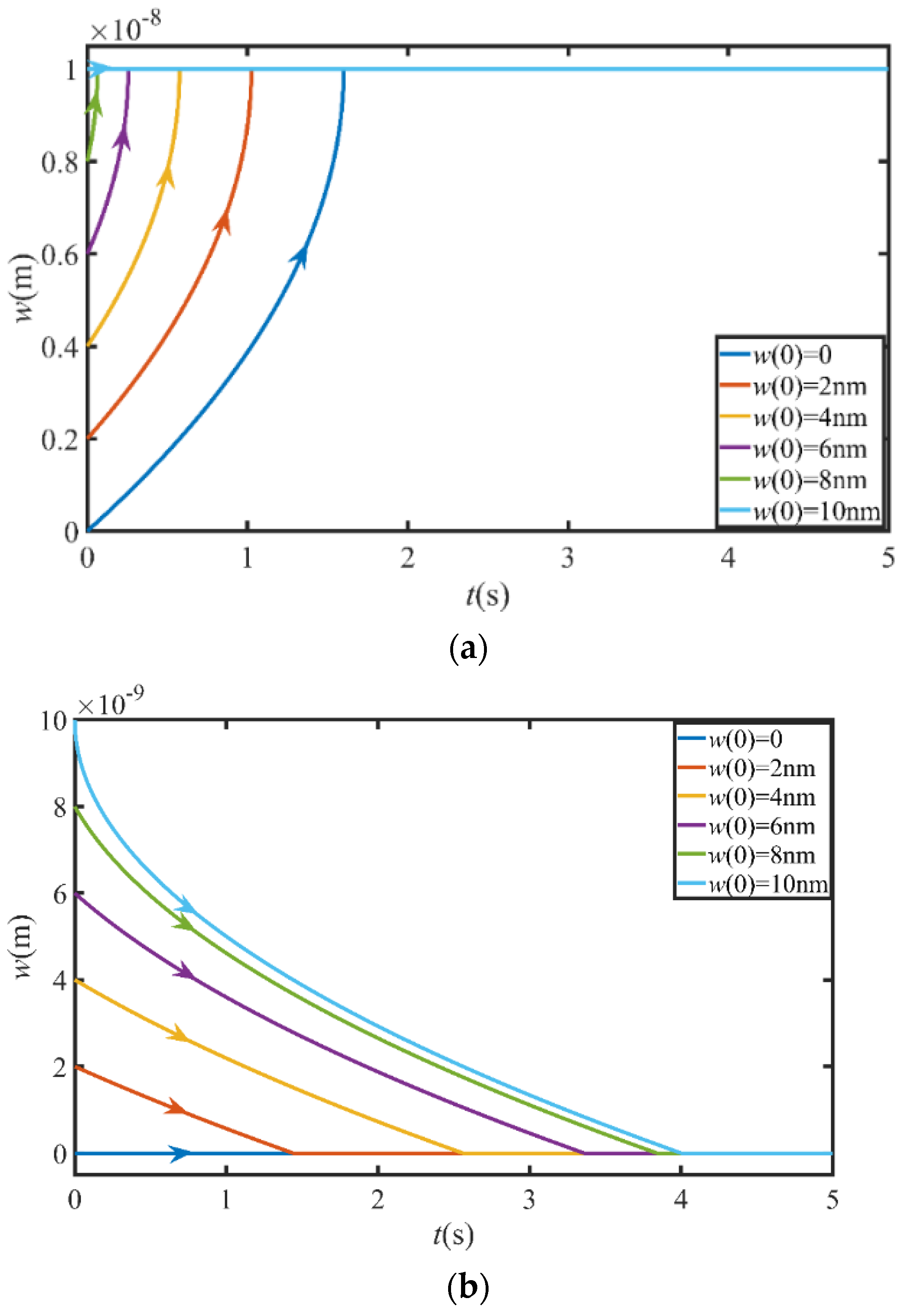
For the HP TiO2 memristor, we have found that the system has two stable equilibrium points: and . Let and . According to Equation (6), the transient response of the memristor is obtained by solving the differential equation numerically, as shown in Figure 2. Figure 2a corresponds to the excitation of the DC voltage, and the memristor responds with different initial values that converge to , i.e., to show the ON resistance . Figure 2b corresponds to . The response of the memristor with different initial values converges to under the excitation of −0.2 V, i.e., to show high resistance . It can be seen from the figure that there are two stable equilibrium points in the memristor.
By using the method mentioned above and substituting the two equilibrium points and of the HP memristor into the first formula in (4), and noting the condition of the existence of the equilibrium point in (6) (, , and , ), the DC response curve can be obtained, as shown in Figure 3.
It can be seen from Figure 3 that the voltage and current correspond one-to-one. When , there is a high resistance ROFF, and when , there is a low resistance RON. The response is independent of the initial value, and there is a history erase phenomenon. The method to derive Figure 3 is the same as [10], where the DC characteristic of a TaO memristor from HP labs was obtained similarly from the Strachan model, presented in [23] after opportune boundary conditions were imposed on the allowable memristor state existence domain.
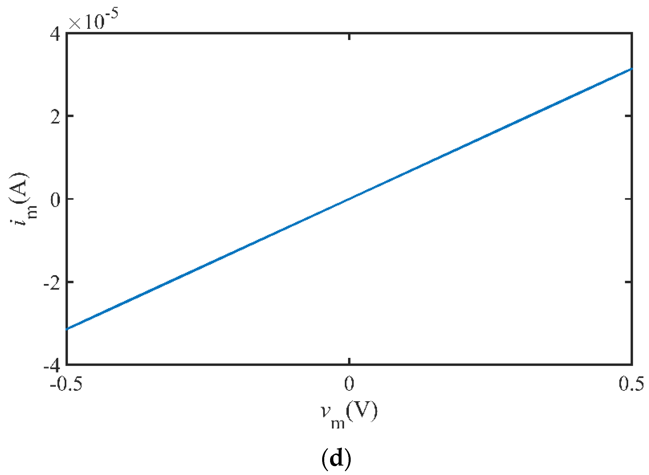
3.2. AC Response
The AC response of the HP TiO2 memristor is studied below. In other words, is substituted into Equation (6) to solve the differential equation with different initial values by a numerical method. The response of the solution is shown in Figure 4. Figure 4a corresponds to f = 1 Hz, which is equivalent to the excitation under quasistatic conditions, and Figure 4c corresponds to f = 10 Hz. The response in both cases shows that there is no history erase effect. In fact, this is predictable. If we look at Figure 1 carefully, we find that the curve family is symmetrical about the horizontal axis, which indicates that the rate of change is symmetrical about the positive and negative swings of the AC signal. Thus, the net contribution of to the state in a signal cycle is 0. Therefore, periodic oscillation should be made around the initial value, and the curve distinguishes with different initial values. It should be noted that the amplitude of the response decreases when frequency increases. This is because the vm − im pinched loop shrinks when the frequency increases (see Figure 4b,d).
3.3. Closed-Form Solution of th eDynamic Equation of the HP TiO2 Memriston
It is observed that the HP TiO2 memristor does not have a history erase effect according to the numerical method above. Next, the response properties of the HP TiO2 memristor are given by a strict mathematical method.
Substituting the first equation of (4) into the second, the following relationship is obtained:
By separating the variables and integrating the two sides, the following results are obtained:
Equation (8) can be further expressed as:
The expression of is obtained by solving the equation.
Note that because holds, we should drop the plus sign in Equation (10). Note also that , and the above formula is simplified as:
Under DC,
By integrating the two sides, we obtain:
Substituting Equation (13) into Equation (11), we obtain:
where
In Formula (14), is a real number and ; therefore, and . If a positive DC voltage V > 0 is applied to the memristor, then T is a monotonic increasing function and a monotonic decreasing function. When the memristor reaches T = 1, reaches the upper limit D; if a negative DC voltage V < 0 is applied to the memristor, T is a monotonic decreasing function and a monotonic increasing function. When T = 0 and , with t increasing, reaches the lower limit of 0.
Although the state variable w in Equation (11) is a function of the initial value w(0), under the excitation of positive and negative DC voltages, the memristor rapidly reaches two states, namely low resistance RON and high resistance ROFF, which are independent of the initial value, indicating that the memristor has a history erase effect. If the memristor is excited by positive and negative pulse voltages, as long as its amplitude and pulse width meet the condition of the state transition, the memristor will become a nonvolatile binary switch device, which can be used in binary memory.
Figure 5 shows the DC response diagram of the memristor state variables when V = 0.5 V and V = − 0.2 V, showing the two limit states under different initial values.
It will be proved that the AC response of the HP memristor has no history erase effect under any AC voltage excitation. When AC voltage is v, we have
by integrating the two sides, we obtain:
substituting Equation (16) into Equation (11) yields:
Because the AC signal vm(t) is arbitrarily chosen, the root term in Equation (17) is not a monotone increasing or decreasing function and is closely related to the initial value w(0) of the memristor. The state variable w(t) is related to the initial value, and there is no history erase effect. Taking the cosine excitation signal as an example, the excitation voltage is assumed to be vm = cos(t), then . Substituting it into Equation (17) will obtain:
It is obvious that the state variable w varies with time t and initial value w(0). Especially when t = kπ, k∈N Equation (18) becomes
depends directly on the initial value , which shows that the AC response of the memristor is related to the initial value, and there is no history erase effect.
3.4. HP TiO2 Memristor Model with a Window Function
The HP memristor model represented by Equation (4) is an ideal model, in which the equation of state is linear, which means that the ions in the doped region move linearly under the external electric field. In practice, however, the drift motion is nonlinear. The boundary effect at the two ends of and especially is strongly nonlinear. In order to describe this nonlinear effect, Strukov added a window function to his memristor model in his original reference [5], and modified the memristor (Equation (4)) into the following form:
By inserting the first formula of Equation (20) with the second, separating variables, and integrating both sides, we obtain:
In (21), the integral is solved and simplified to
when DC excitation is applied:
By integrating the two sides, we obtain:
Substituting Equation (24) into Equation (22), we obtain the following results:
If a positive voltage is applied and the right side of the equation is an increasing function of t, which tends to infinity after a period of time, then there must be on the left side of the equation; if a negative voltage is applied and the right side of the equation is a decreasing function of t and tends to 0 after a period of time, then there must be on the left side of the equation. It can be seen that under the excitation of positive and negative DC voltages, the memristor state variables w tend to D and 0, respectively; that is, the memristor is in RON and ROFF states, respectively, and its response is independent of the initial value.
When an AC cosine voltage is applied, Equation (24) becomes . Let the responses of the state variable under two different initial values, respectively, be and , which can be substituted into Equation (22) and divided:
when , if tends to , the left side of Equation (26) is 1, while the right side is equal to a constant, which is not 1:
In this case, Equation (26) would not hold, i.e., . Therefore, there is no history erase effect in the memristor.
3.5. Parasitic Memcapacitance Effect of the HP TiO2 Emristor
If we further observe the structure of the HP TiO2 memristor, we will find that there is a parasitic parallel plate capacitor in the memristor; in fact, as shown next, it is a memcapacitor, because the capacitance is dependent on state variable w, and the dielectric between the two plates is undoped TiO2. This is because undoped TiO2 has a higher resistivity, equivalent to an insulator medium, while doped TiO2 has a lower resistivity, equivalent to a conductor, as shown in Figure 6.
The parasitic capacitance is equivalent to a flat-plate capacitor, and because the capacitance is dependent on state variable w(t), it is indeed a memcapacitor:
According to [24], we know , . When the parasitic memcapacitance is considered, by KCl and KVL, we have:
where is the voltage across both ends of the capacitor, and is the derivative of capacitance to time. Expression (28) of capacitance is substituted into the second equation of (29), and then the second equation is substituted into the first equation and the third equation into the forth, and Equation (30) is obtained:
According to Equation (30), the AC response of state variable to t is solved by MATLAB and shown as Figure 7. The excitation signal in the diagram is , is selected as 0.5 V, and f is set to 10 Hz.
It can be seen from the figure that under different initial values, the AC response converges to a stable value after a period of time, so there is a history erase effect.
4. The Self-Directed Channel (SDC) Memristor
The Self-Directed Channel (SDC) memristor is a product developed by Knowm Company. This is an ion conduction device (also known as an electrochemical metallization (ECM) device), which changes the resistance of the device by relying on Ag+ entering the channel of the active layer of the device. The hysteretic curve can be measured by software and hardware tools provided by Knowm Company. However, there is no mathematical model. In order to analyze it theoretically and design a memristor circuit with it, it is necessary to establish a mathematical model for it.
4.1. Establishment of the SDC Memristor Model
In his 2015 paper [20], Kvatinsky proposed a generic voltage-controlled memristor model VTEAM. The model’s equation is as follows:
The equation has ten parameters, where are real numbers, and are natural numbers. are the boundaries of the internal variable w, and are resistance values when the values of state variable are , respectively. are constants, and are the threshold voltages.
VTEAM model is a generic model. Because of its inherent universality and robustness, it can be applied to a large number of memristor models and experimental data. Considering the current voltage characteristics of a specific memristor, a set of parameters are selected to make the VTEAM model conform to the reference I–V relationship of the SDC memristor. In order to determine the I–V curve, simulated annealing algorithms can be used to minimize the relative root mean square error. The relative root mean square error is
where N is the number of samples, and are the sampling voltage and current values of the VTEAM model, respectively, and and are the actual measured sampling voltage and current values, respectively.
The fitting process is to make the program iterate over to minimize the error function given in (33). In order to avoid convergence to the local minimum instead of the best global fit, other parameters () are selected manually to show as much similarity as possible to the reference I–V relationship (relative root mean square error is less than 1.5%). In addition, the ideal window function can be used to constrain the state variables in the process of fitting.
In the experiment, the memristor is connected with a 1KΩ resistor in series and an applied AC signal as . Considering that only part of the voltage falls on the memristor, can be taken as 1 V, and the frequency f can be set to 5 Hz. After the volt–ampere data are obtained, the data are imported into MATLAB, and the simulated annealing algorithm is used to set the objective function to (34).
The VTEAM model was used to fit the experimental data, and Figure 8 was obtained. Looking at Figure 8, it can be found that the model fitting is very good in the first quadrant, while there is a little difference between the fitting data and the measured data in the third quadrant. This is mainly due to the insufficient sampling accuracy of the measurement software and hardware provided by Knowm Company (200 time points in total).
According to the computer simulation, the optimal parameters of the model can be determined as shown in Table 1.
4.2. Dynamic Routes and AC Response of the SDC Memristor
According to the model parameters, the dynamic routes of the SDC memristor can be drawn in a similar way to that of the HP TiO2 memristor and shown as Figure 9. It is noted that in Equation (32), does not depend on w but only on . Therefore, vs. w is a set of horizontal lines.
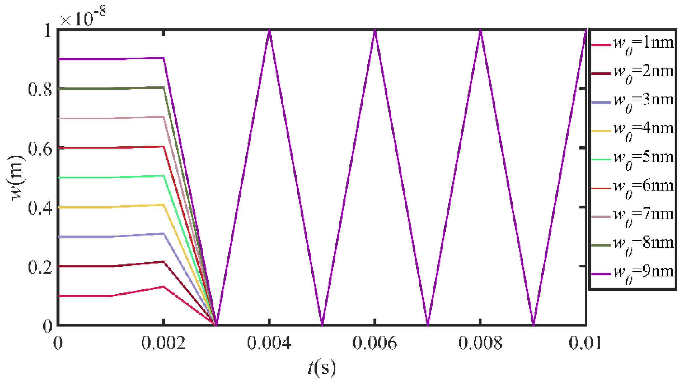
It can be seen from the diagram that the dynamic routes are asymmetric with respect to the horizontal axis, which indicates that the net contribution of to w is not zero when the signal amplitude is positive and negative for one cycle under AC excitation. Therefore, it is speculated that under AC excitation, may gradually tend to a stable value after a period of time under the state of net increase or decrease of , thus it has a history erase effect. We use a sinusoidal signal , where f is 5 Hz and with as the AC excitation and applied to the memristor. Thus, Figure 10 can be obtained. It can be seen from Figure 10 that the SDC memristor has a history erase effect under AC conditions.
4.3. Considering the Parasitic Capacitance Effect
Similar to the case of the HP TiO2 memristor (refer to Figure 6), considering that the undoped part is also equivalent to a moving parallel plate capacitor, it can be considered to have parallel a small parasitic capacitor on it. Assuming 1nF, the circuit equation becomes:
The solution of the state variable w(t) can be obtained by numerically solving the above differential equation with MATLAB, as shown in Figure 11.
5. Conclusions
In this paper, the history erase effect of the HP TiO2 memristor is studied. Firstly, the existence of the history erase effect under DC and AC conditions is predicted from the dynamic routes. The historical erase properties of the HP TiO2 memristor under AC and DC are then verified by a MATLAB numerical simulation. It can be seen that the HP TiO2 memristor has a DC history erase effect but no AC history erase effect. After the numerical simulation, the closed-form solution of the dynamic equation of the TiO2 memristor is given. Thus, the history erase properties of the TiO2 memristor under DC and AC conditions are explained theoretically. Furthermore, the parasitic capacitance effect of the HP TiO2 memristor is considered, and it is pointed out that the parasitic capacitance effect can cause the HP TiO2 memristor to have an AC history erase effect. It is worth noting that Menzel et al. pointed out that the resistance of the doping region in the memristor is the origin of history erase effect [13]. From the work of this paper, it seems that the resistance of the doped region and the parasitic memcapacitance of the undoped region work together to form a discharge path, which leads to the history erase effect. As a supplement to the research work on the history erase effect of the HP TiO2 memristor, we studied the history erase effect of the latest discrete SDC memristor made by Knowm Company. The DC and AC voltages and parasitic capacitance are considered, respectively. It is worth mentioning that the method of modeling the SDC memristor with the generic voltage-controlled memristor model VTEAM is also given in this paper. This method uses a simulated annealing algorithm to fit the actual measured data, which solves the problem that Knowm Company’s discrete SDC memristor still lacks an accurate mathematical model. It can be seen that no matter with and without the parasitic capacitance, the SDC memristor has an AC history erase effect.
Author Contributions
Numerical simulation, theoretical calculation and manuscript writing, Y.S.; supervision, G.W. All authors have read and agreed to the published version of the manuscript.
Funding
This research was funded by The National Natural Science Foundation of China (NNSFC), grant number 61771176.
Conflicts of Interest
The authors declare no conflict of interest. The funders had no role in the design of the study; in the collection, analyses, or interpretation of data; in the writing of the manuscript, or in the decision to publish the results.
References
- Maikap, S.; Banerjee, W. In Quest of Nonfilamentary Switching: A Synergistic Approach of Dual Nanostructure Engineering to Improve the Variability and Reliability of Resistive Random-Access-Memory Devices. Adv. Electron. Mater. 2020. [Google Scholar] [CrossRef]
- Ginnaram, S.; Qiu, J.T.; Maikap, S. Role of the Hf/Si Interfacial Layer on the High Performance of MoS2-Based Conductive Bridge RAM for Artificial Synapse Application. IEEE Electron. Device Lett. 2020, 41, 709–712. [Google Scholar] [CrossRef]
- Li, H.; Hu, M. Compact model of memristors and its application in computing systems. In Proceedings of the 2010 Design, Automation & Test in Europe Conference & Exhibition (DATE 2010), Dresden, Germany, 8–12 March 2010; pp. 673–678. [Google Scholar] [CrossRef]
- Chua, L. Memristor-The missing circuit element. IEEE Trans. Circuit Theory 1971, 18, 507–519. [Google Scholar] [CrossRef]
- Strukov, D.B.; Snider, G.S.; Stewart, D.R.; Williams, R.S. The missing memristor found. Nature 2008, 453, 80–83. [Google Scholar] [CrossRef]
- Dong, Z.; Lai, C.S.; He, Y.; Qi, D.; Duan, S. Hybrid dual-complementary metal-oxide-semiconductor/memristor synapse-based neural network with its applications in image super-resolution. IET Circuits Devices Syst. 2019, 13, 1241–1248. [Google Scholar] [CrossRef]
- Dong, Z.; Lai, C.S.; Qi, D.; Xu, Z.; Li, C.; Duan, S. A general memristor-based pulse coupled neural network with variable linking coefficient for multi-focus image fusion. Neurocomputing 2018, 308, 172–183. [Google Scholar] [CrossRef]
- Dong, Z.; Qi, D.; He, Y.; Xu, Z.; Hu, X.; Duan, S. Easily Cascaded Memristor-CMOS Hybrid Circuit for High-Efficiency Boolean Logic Implementation. Int. J. Bifurc. Chaos 2018, 28, 1850149. [Google Scholar] [CrossRef]
- Boyd, S.; Chua, L. Fading memory and the problem of approximating nonlinear operators with Volterra series. IEEE Trans. Circuits Syst. 1985, 32, 1150–1161. [Google Scholar] [CrossRef] [Green Version]
- Ascoli, A.; Tetzlaff, R.; Chua, L.O.; Strachan, J.P.; Williams, R.S. History Erase Effect in a Non-Volatile Memristor. IEEE Trans. Circuits Syst. I Regul. Pap. 2016, 63, 389–400. [Google Scholar] [CrossRef]
- Ascoli, A.; Tetzlaff, R.; Chua, L.O. The First Ever Real BistableMemristors—Part I: Theoretical Insights on Local Fading Memory. IEEE Trans. Circuits Syst. II Express Briefs 2016, 63, 1091–1095. [Google Scholar] [CrossRef]
- Ascoli, A.; Tetzlaff, R.; Chua, L.O. The First Ever Real BistableMemristors—Part II: Design and Analysis of a Local Fading Memory System. IEEE Trans. Circuits Syst. II Express Briefs 2016, 63, 1096–1100. [Google Scholar] [CrossRef]
- Menzel, S.; Waser, R.; Siemon, A.; La Torre, C.; Schulten, M.; Ascoli, A.; Tetzlaff, R. On the origin of the fading memory effect in ReRAMs. In Proceedings of the 2017 27th International Symposium on Power and Timing Modeling, Optimization and Simulation (PATMOS), Thessaloniki, Greece, 25–27 September 2017; pp. 1–5. [Google Scholar] [CrossRef]
- Ascoli, A.; Ntinas, V.; Tetzlaff, R.; Sirakoulis, G.C. Closed-form analytical solution for on-switching dynamics in a TaOmemristor. Electron. Lett. 2017, 53, 1125–1126. [Google Scholar] [CrossRef]
- Ascoli, A.; Tetzlaff, R.; Menzel, S. Exploring the Dynamics of Real-World Memristors on the Basis of Circuit Theoretic Model Predictions. IEEE Circuits Syst. Mag. 2018, 18, 48–76. [Google Scholar] [CrossRef]
- Campbell, K.A. Self-directed channel memristor for high temperature operation. Microelectron. J. 2017, 59, 10–14. [Google Scholar] [CrossRef]
- Drake, K.; Lu, T.; Majumdar, M.; Kamrul, H.; Campbell, K.A. Comparison of the Electrical Response of Cu and Ag Ion-Conducting SDC Memristors Over the Temperature Range 6 K to 300 K. Micromachines 2019, 10, 663. [Google Scholar] [CrossRef] [Green Version]
- Gomez, J.; Vourkas, I.; Abusleme, A.; Sirakoulis, G.C.; Rubio, A. Voltage Divider for Self-Limited Analog State Programing of Memristors. IEEE Trans. Circuits Syst. II Express Briefs 2020, 67, 620–624. [Google Scholar] [CrossRef]
- Gomez, J.; Vourkas, I.; Abusleme, A. Exploring Memristor Multi-Level Tuning Dependencies on the Applied Pulse Properties via a Low Cost Instrumentation Setup. IEEE Access 2019, 7, 59413–59421. [Google Scholar] [CrossRef]
- Kvatinsky, S.; Ramadan, M.; Friedman, E.G.; Kolodny, A. VTEAM: A General Model for Voltage-Controlled Memristors. IEEE Trans. Circuits Syst. II Express Briefs 2015, 62, 786–790. [Google Scholar] [CrossRef]
- Kvatinsky, S.; Friedman, E.G.; Kolodny, A.; Weiser, U.C. TEAM: ThrEshold Adaptive Memristor Model. IEEE Trans. Circuits Syst. I Regul. Pap. 2013, 60, 211–221. [Google Scholar] [CrossRef]
- Williams, R.S. How We Found the Missing Memristor. IEEE Spectr. 2008, 45, 28–35. [Google Scholar] [CrossRef]
- Strachan, P.; Torrezan, A.C.; Miao, F.; Pickett, M.D.; Yang, J.J.; Yi, W.; Medeiros-Ribeiro, G.; Williams, R.S. State dynamics and modelling of Tantalum oxide memristors. IEEE Trans. Electron Devices 2013, 60, 2194–2202. [Google Scholar] [CrossRef]
- Pickett, M. The Materials Science of Titanium Dioxide Memristors. Ph.D. Thesis, University of California, Berkeley, CA, USA, 2010. [Google Scholar]
Figure 1.
The dynamic route of the Hewlett-Packard (HP) TiO2 memristor, in which the red line is the power-off plot (POP); that is, the relationship between and w when the voltage is 0. (b) Local zoom-in of (a). Note that the small circles in the curve indicate that the curve cannot obtain the value of that point.

Figure 2.
Transient response of the memristor under DC. (a) Corresponding voltage ; (b) corresponding voltage . The initial value is w0∈ {0, 1 nm, 2 nm, 3 nm, 4 nm, 5 nm, 6 nm, 7 nm, 8 nm, 9 nm, 10 nm}.
Figure 2.
Transient response of the memristor under DC. (a) Corresponding voltage ; (b) corresponding voltage . The initial value is w0∈ {0, 1 nm, 2 nm, 3 nm, 4 nm, 5 nm, 6 nm, 7 nm, 8 nm, 9 nm, 10 nm}.

Figure 3.
DC response of the HP TiO2 memristor.

Figure 4.
is used as the excitation signal, where (a) corresponds to f = 1 Hz, equivalent to the excitation under quasistatic conditions; (b) corresponds to the locus of vm − im at f = 1 Hz; (c,d) correspond to f = 10 Hz.
Figure 4.
is used as the excitation signal, where (a) corresponds to f = 1 Hz, equivalent to the excitation under quasistatic conditions; (b) corresponds to the locus of vm − im at f = 1 Hz; (c,d) correspond to f = 10 Hz.


Figure 5.
DC response diagram of the memristor, according to Equation (15). (a) Under a positive voltage , the responses of initial values are obtained. (b) Under a negative voltage , the responses of initial values are obtained.
Figure 5.
DC response diagram of the memristor, according to Equation (15). (a) Under a positive voltage , the responses of initial values are obtained. (b) Under a negative voltage , the responses of initial values are obtained.

Figure 6.
Structure of the HP TiO2 memristor.

Figure 7.
AC response of state variable w(t) to t considering parasitic memcapacitance, in which the excitation signal is vm (t) = V0 sin(2πft), V0 is selected as 0.5 V, and f is set to 10 Hz.
Figure 7.
AC response of state variable w(t) to t considering parasitic memcapacitance, in which the excitation signal is vm (t) = V0 sin(2πft), V0 is selected as 0.5 V, and f is set to 10 Hz.

Figure 8.
Volt–ampere characteristic curve of memristor. Red is the experimental data, blue is the model fitting data under the optimization algorithm.
Figure 8.
Volt–ampere characteristic curve of memristor. Red is the experimental data, blue is the model fitting data under the optimization algorithm.

Figure 9.
Dynamic routes of the Self-Directed Channel (SDC) memristor. Tote that POP (vm = 0) and the line corresponding to vm = 0.1 V are in fact two different lines.
Figure 9.
Dynamic routes of the Self-Directed Channel (SDC) memristor. Tote that POP (vm = 0) and the line corresponding to vm = 0.1 V are in fact two different lines.

Figure 10.
Sinusoidal signal , with f = 5 Hz and = as the AC excitation and applied to the memristor (a) can be obtained, (b) corresponds to =.
Figure 10.
Sinusoidal signal , with f = 5 Hz and = as the AC excitation and applied to the memristor (a) can be obtained, (b) corresponds to =.

Figure 11.
AC response with parasitic capacitance taken into account. Using sinusoidal signal , with f = 5 Hz and = 0.5 V as the AC excitation, (a) is obtained. (b) corresponds to =.
Figure 11.
AC response with parasitic capacitance taken into account. Using sinusoidal signal , with f = 5 Hz and = 0.5 V as the AC excitation, (a) is obtained. (b) corresponds to =.


Table 1.
Model parameters obtained by the simulation of the optimization algorithm.
| Parameters | Value |
|---|---|
| 14.277 kΩ | |
| 1.5936 kΩ | |
| 0.02 V | |
| −0.13 V | |
| 538,530.50 nm | |
| −2.6213 m | |
| 2 | |
| 8 | |
| 0 | |
| 0.001 m |
Publisher’s Note: MDPI stays neutral with regard to jurisdictional claims in published maps and institutional affiliations. |
© 2021 by the authors. Licensee MDPI, Basel, Switzerland. This article is an open access article distributed under the terms and conditions of the Creative Commons Attribution (CC BY) license (http://creativecommons.org/licenses/by/4.0/).
Share and Cite
MDPI and ACS Style
Shen, Y.; Wang, G. History Erase Effect of Real Memristors. Electronics 2021, 10, 303. https://doi.org/10.3390/electronics10030303
AMA Style
Shen Y, Wang G. History Erase Effect of Real Memristors. Electronics. 2021; 10(3):303. https://doi.org/10.3390/electronics10030303
Chicago/Turabian StyleShen, Yiran, and Guangyi Wang. 2021. "History Erase Effect of Real Memristors" Electronics 10, no. 3: 303. https://doi.org/10.3390/electronics10030303
Note that from the first issue of 2016, this journal uses article numbers instead of page numbers. See further details here.