Article

Photovoltaic Power Plant Collection and Connection to HVDC Grid with High Voltage DC/DC Converter

1
Laboratory of Renewable Energy, Institute of Electrical Engineering, Chinese Academy of Sciences, Beijing 100190, China
2
School of Electronics, Electrical and Communication Engineering, University of Chinese Academy of Sciences, Beijing 100049, China
*
Author to whom correspondence should be addressed.
Electronics 2021, 10(24), 3098; https://doi.org/10.3390/electronics10243098
Submission received: 18 November 2021 / Revised: 1 December 2021 / Accepted: 8 December 2021 / Published: 13 December 2021
(This article belongs to the Special Issue Grid-Connected PV Systems)

Abstract

:
Photovoltaic (PV) power plant collection and connection to a high voltage direct current (HVDC) grid has many advantages. Compared with the traditional AC collection and grid-connection scheme, it can reduce the power conversion links and improve the system efficiency. As one of the most important devices in the application of a PV HVDC collection and grid-connection system, a high voltage, large capacity, high step-up ratio DC/DC converter is the critical technology. A DC/DC converter scheme based on a boost full bridge isolated power module cascaded in input parallel output series (IPOS) structure is proposed to meet the technical requirements of PV power conversion with high voltage, large capacity, and high step-up ratio. The operation mode of the power module is analyzed, the soft switching method is proposed, and the constraint to realize the soft switching of the power module is deduced. Aiming to resolve the problem of multi-module voltage and current equalization in a cascaded DC/DC converter, a distributed module equalization control strategy is proposed to realize the reliable operation of a power module and converter. A 5 kV/80 kW standard power module is developed, the DC/DC converter experimental platform is built, and the proposed system scheme and control strategy are verified by experiments. Based on a 14-power module input parallel output series connection, a ±30 kV/1 MW PV DC/DC converter is developed, a ±30 kV PV HVDC collection and grid-connection demonstration system is established, and the experimental test is completed to realize the stable operation of the system.

1. Introduction

The large-scale development and utilization of photovoltaic (PV), wind power, and other renewable energies are important solutions to solve the energy crisis and environmental problems [1]. In the past decades, the new installed PV power plant capacity in the world has increased year by year. The scale of PV power plants is developing in the direction of a large-scale, centralized, and PV power generation base, and the capacity of a single PV power plant is from tens of megawatts (MW) to hundreds of MW [2]. As shown in Figure 1a, the low voltage alternating current (AC) scheme is usually adopted in the traditional PV power plant to realize PV power collection. More specifically, the box transformer and main transformer are used to realize the multi-stage step-up voltage, before the PV power plant is connected to the medium voltage (MV) or high voltage (HV) AC grid [3]. Since the PV power plant AC collection and grid-connection scheme requires multi-stage power conversion equipment and transformation links, it is difficult to reduce system costs and improve system efficiency [4]. Meanwhile, with the large-scale and centralized PV power plant connected to the AC grid, the traditional AC collection and grid-connection scheme has several problems, such as harmonic resonance, synchronous oscillation, large capacity reactive power compensation, etc., which become the technical bottleneck of large-scale PV power plant development [5,6].
With the rapid development of the flexible HVDC transmission technology, the PV DC boost collection and DC grid-connection scheme is proposed [7,8]. The scheme, shown in Figure 1b, can effectively avoid the problems of a traditional PV power plant AC collection and grid-connection scheme. Moreover, the PV HVDC collection and grid-connection will reduce the power conversion links, save the power conversion equipment, reduce system cost, and improve the overall efficiency of the system as well. To sum up, a PV power plant with a HVDC collection and grid-connection scheme has many obvious economic and technological advantages [9].
As the main interconnection equipment between the PV array and the HVDC grid, there are several critical technical requirements and challenges of the DC/DC converter for the PV array connected to the HVDC grid, which has become a research hotspot in recent years [10]. The technical requirements of the DC/DC converter for large-scale renewable energy collection applications are studied, and it is pointed out that the DC/DC converter should have the characteristics of high voltage, high voltage gain, large capacity, and unidirectional power flow [11]. Meanwhile, the DC/DC converter must have high reliability and efficiency as the traditional grid-connected inverter and transformers. Traditional low voltage two-level DC/DC converter topologies cannot directly meet the HV application technical requirements due to the limitations of voltage and current capacity of semiconductor power devices, and the insulated gate bipolar translator (IGBT) series scheme suffers from the dynamic voltage and current sharing problem [12].
A modular multi-level converter (MMC) scheme is an effective solution for high voltage and large capacity applications. Several types of MMC-DC/DC converters are studied, including the isolated MMC-DC/DC converter and the non-isolated MMC-DC/DC converter [13]. From the perspective of safety, because there is no transformer isolation, a non-isolated MMC-DC/DC converter cannot achieve the requirements of galvanic isolation and fault isolation [14]. The isolated MMC-DC/DC converter is better than the non-isolated one and usually adopts a line frequency transformer to step-up voltage and achieve galvanic isolation. However, the line frequency transformer is bulky. Therefore, the transformer with low frequency from 300 Hz to 1000 Hz are proposed to replace the line frequency transformer. In this situation, the problems of large core loss and high equivalent switching frequency of the transformer cannot be avoided, which limits the application of high voltage and high power. At the same time, MMC-DC/DC converter structure requires hundreds of MMC modules, which result to large volume, high cost and complex control. Consequently, it is only suitable for the specific application scenarios, especially in DC power grid interconnection [15].
A modular cascaded DC/DC converter is another effective technical scheme to realize high voltage, large capacity, and high step-up ratio, especially the input parallel output series (IPOS) module cascade structure, which is suitable for high power conversion from low voltage to high voltage. It can not only use the existing low voltage power devices and power conversion topology, but also facilitates the improvement of system reliability and capacity expansion and meets the technical requirements for PV HVDC collection and grid-connection application [16].
As the core of the IPOS cascaded DC/DC converter, the operating characteristics of the power module directly determine the performance of the DC/DC converter [17]. At the same time, the inconsistency of hardware parameters between power modules will cause the imbalance of input current and output voltage between modules in the DC/DC converter, which will seriously affect the reliable operation of the converter [18]. Therefore, it is necessary to select the appropriate power module topology of DC/DC converter for PV HVDC collection and grid-connection. Meanwhile, the input current or output voltage equalization between modules needs to be controlled to ensure the stable operation of power modules and the converter. In [19], a modular cascaded DC converter is proposed, and the power module uses two-stage power conversion topology, which requires many components and complex coordination control between the two stages. In [20], an IPOS DC/DC converter is proposed based on dual active bridge (DAB) topology, but both sides of the converter adopt active power devices, so the control is relatively complex [20]. Literature [21,22] studies the voltage and current sharing control strategy of the IPOS cascaded DC/DC converter, but these are all realized based on the voltage and current equalization command sent by the centralized controller. Once the number of operating modules changes, the equalization command needs to be adjusted in time according to the actual number of operating modules. If the converter fails to obtain module fault information in time, the incorrect equalization command will be generated, and the converter will not operate normally.
From the analysis above, it is concluded that the DC/DC converter studied in the current literature cannot fully meet the technical requirements for large-scale PV power plant DC collection and connection to HVDC grid application. The high step-up ratio, high voltage, and large capacity are the critical problems facing a PV DC/DC converter connected to the HVDC grid. Meanwhile, due to the PV maximum power point tracking (MPPT) voltage random variation in the wide range of 450V~850V, the DC/DC converter operates under the condition of variable step-up ratio. Therefore, it is mandatory to study the DC/DC converter of higher voltage, larger capacity and variable step-up ratio and high efficiency.
In this paper, firstly, the structure of PV power plant HVDC collection and grid-connection system is illustrated. According to the application requirements of PV HVDC collection and grid-connection DC/DC converter, a boost full bridge isolated standard power module-based input parallel output series cascaded converter is proposed and high voltage, large capacity, and high step-up ratio of the PV power conversion are realized. The wide input voltage range soft switching strategy of the proposed DC/DC converter is analyzed and the constraint condition of the soft switching realization is deduced. Secondly, the basic control strategy of the PV DC/DC converter is illustrated, and a distributed module equalization control strategy of the IPOS cascaded converter is proposed, which can effectively reduce the centralized control instructions, improve the reliability of converter equalization control, and realize the stable operation of the power module and converter. Finally, the 5 kV/80 kW standard power module is developed. Based on fourteen 5 kV/80 kW standardized power modules, an engineering prototype of a ±30 kV/1 MW DC/DC converter was completed, and the converter was demonstrated in a PV HVDC collection and grid-connection system. Experimental results and demonstration system test results verified the proposed DC/DC converter and control strategy.

2. Topology of High Voltage, Large Capacity, High Step-Up Ratio DC/DC Converter

2.1. Sructure of PV HVDC Collection and Grid-Connection System

A PV HVDC grid connected system realizes PV power collection and voltage step-up through DC/DC converter of PV generation unit, making the output voltage directly reach the appropriate transmission voltage level. The typical structure of a HVDC collection and grid-connection PV power plant system is shown in Figure 2. As the counterpart of the AC system, the HVDC collection and grid-connection scheme is able to reduce the power conversion links, as well as save the power conversion equipment and system cost. The efficiency of HVDC collection and grid-connection scheme can improve around 3%.
Generally, the PV array takes 500 kW or 1 MW as a unit, and a PV generation unit is composed of a PV array and a DC/DC converter. The collection of PV power can be realized by parallel connection of the output of the PV generation units, and then the PV power is transmitted to the HVDC grid through the HVDC transmission line. The HVDC bus voltage of the collection and grid-connected system is controlled by the HVDC grid. Each PV generation unit in the system only needs to control the output current of the converter to control the PV grid-connected power.

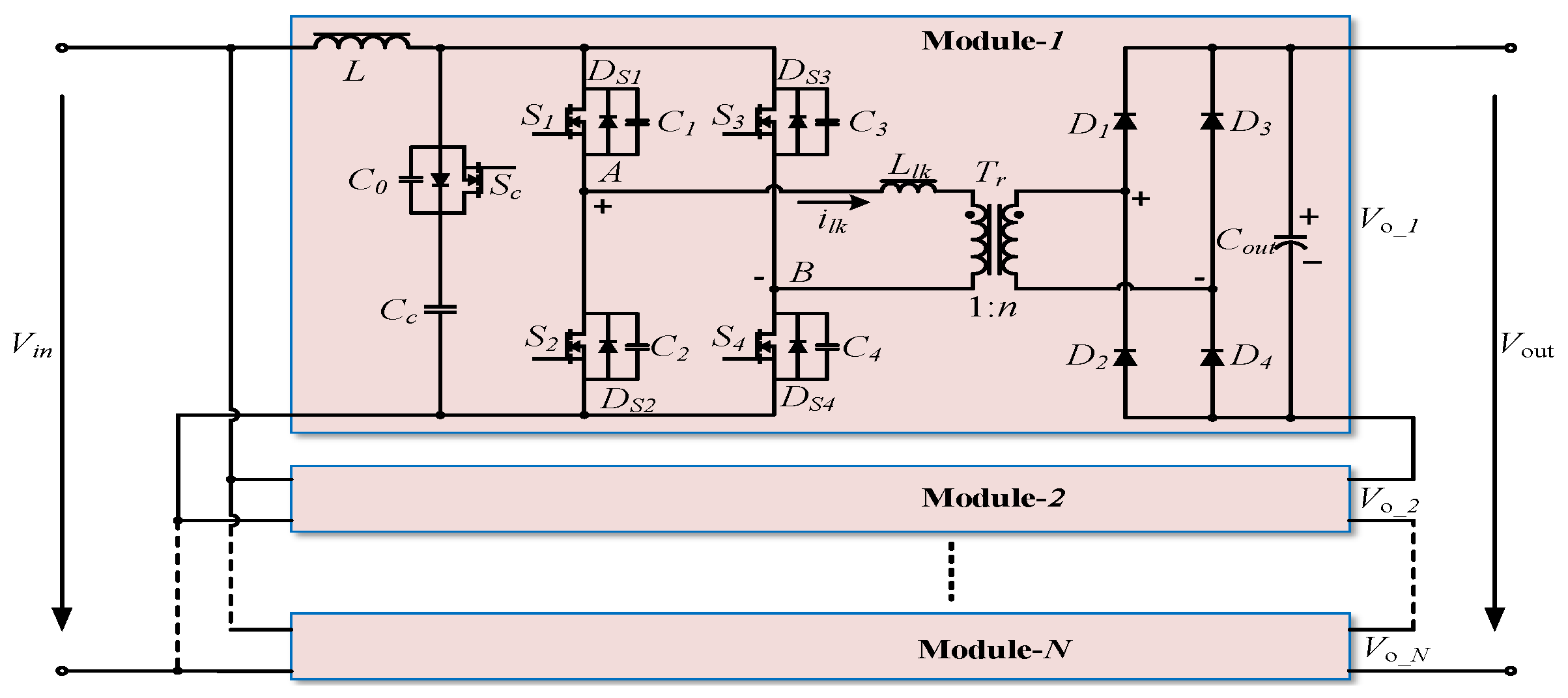
2.2. Modular Cascaded DC/DC Converter Based on Boost Full Bridge Isolated Topology

According to the requirements of a PV HVDC collection and grid-connection system, the DC/DC converter has to meet the characteristics of high voltage, large capacity, high step-up ratio, galvanic isolation, and high efficiency. In this paper, a modular IPOS cascaded scheme based on a boost full bridge isolated converter (BFBIC) topology is proposed to realize the high voltage gain from low voltage PV to a HVDC grid. Figure 3 shows the structure of the proposed IPOS modular cascaded DC/DC converter based on the boost full bridge isolated topology, which is suitable for high voltage gain, wide input voltage range, and high-power applications. To reduce the voltage stress and switching losses of the switches and improve the efficiency of the converter, the active clamp circuit is used to suppress the H-bridge switches turning-off voltage spike and the soft switching is proposed to realize the switches zero voltage switching (ZVS). The active clamp circuit is composed of switch S0 and clamping capacitor CC, L is boost inductor, switch S1, S2, S3, S4, and their anti-parallel diodes constitute a full bridge circuit, Tr is high frequency isolation transformer, n is the transformer turns ratio, Llk is the transformer equivalent leakage inductance, four rectifier diodes D1, D2, D3, D4 constitute a full bridge rectifier circuit, and Cout is the output side capacitor.
The control sequence of BFBIC topology with active clamping circuit is shown in Figure 4. According to the operating characteristics of the boost full bridge isolated topology, the duty cycle of H-bridge power switches meets 0.5 < D < 1. The symmetrical PWM control mode is adopted, that is, the trigger pulse signal of diagonal switches are consistent, and the phase shift between S1, S4 and S2, S3 is 180°. When the power switches S1, S4 or S2, S3 are turned off, the clamping switch S0 is turned on to share the inductive current and suppress the H-bridge switches turning off voltage spike.
The voltage gain Gm between input voltage and output voltage of boost full bridge isolated power module can be written as:
G m = V o V i n = n 2 ( 1 D )
where Vin represents the input voltage of the power module, Vo represents the output voltage of the power module, n is the turns ratio of the high frequency transformer, and D is the duty cycle of the power module H-bridge switches.
The duty cycle of the power module is greater than 0.5, considering the ratio of the high frequency transformer is 5.88, the power module can achieve about 12 times voltage gain when the duty cycle D = 0.75. Therefore, large voltage gain is obtained from the module level.
The multi-module cascaded IPOS converter voltage gain Gc with boost full bridge isolated power module can be written as:
G c = V o u t V i n = n 2 ( 1 D ) M
where Vout represents the output voltage of the IPOS DC/DC converter and M is the number of internal cascaded modules of the IPOS DC/DC converter.
Through the input parallel output series cascaded of power module, the converter with high voltage, large capacity and high step-up ratio is realized. At the same time, through the flexible adjustment of duty cycle, the variable step-up ratio of the converter can be realized to meet the requirements of maximum power point tracking in a wide voltage range of the PV array.

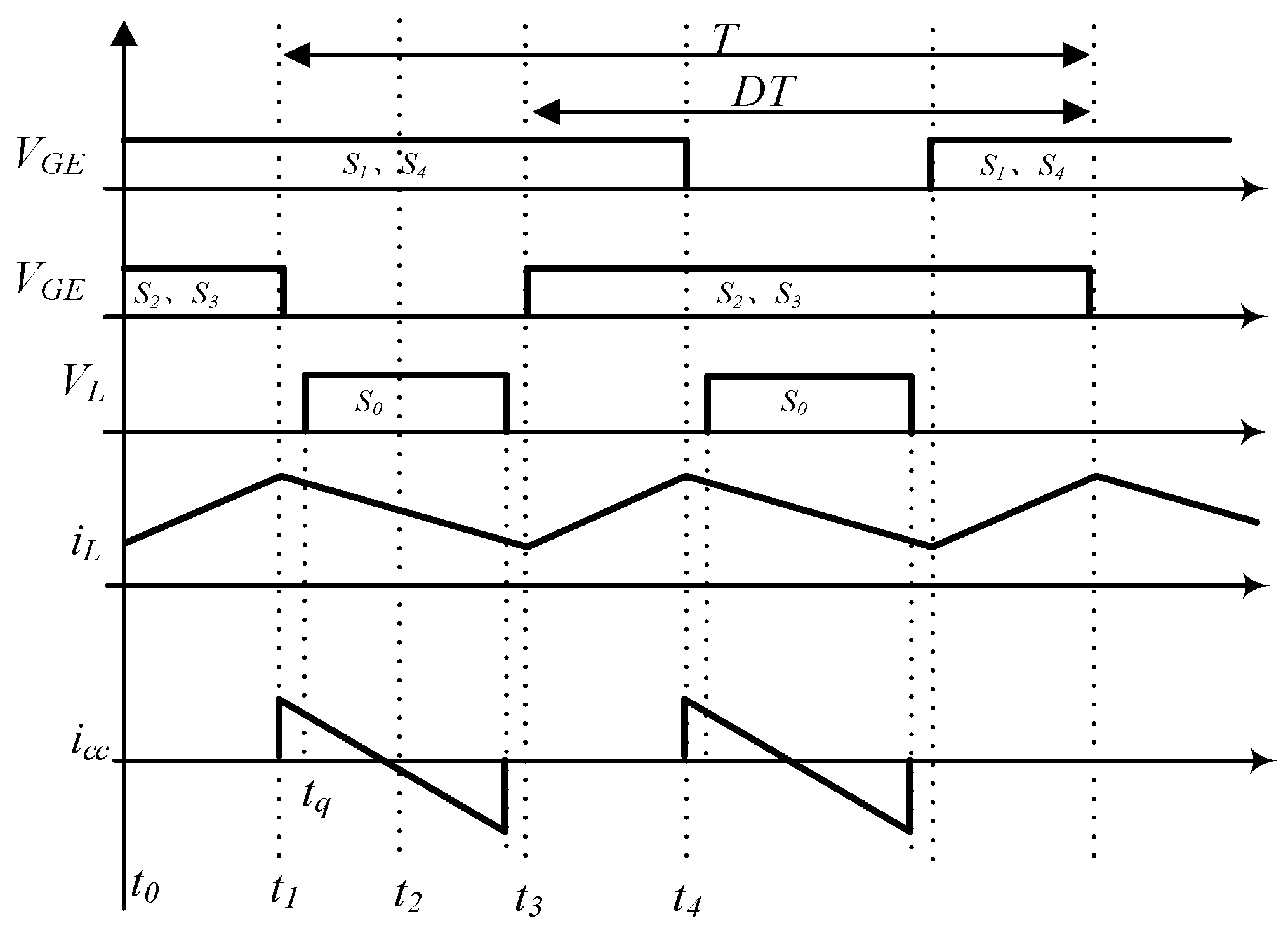
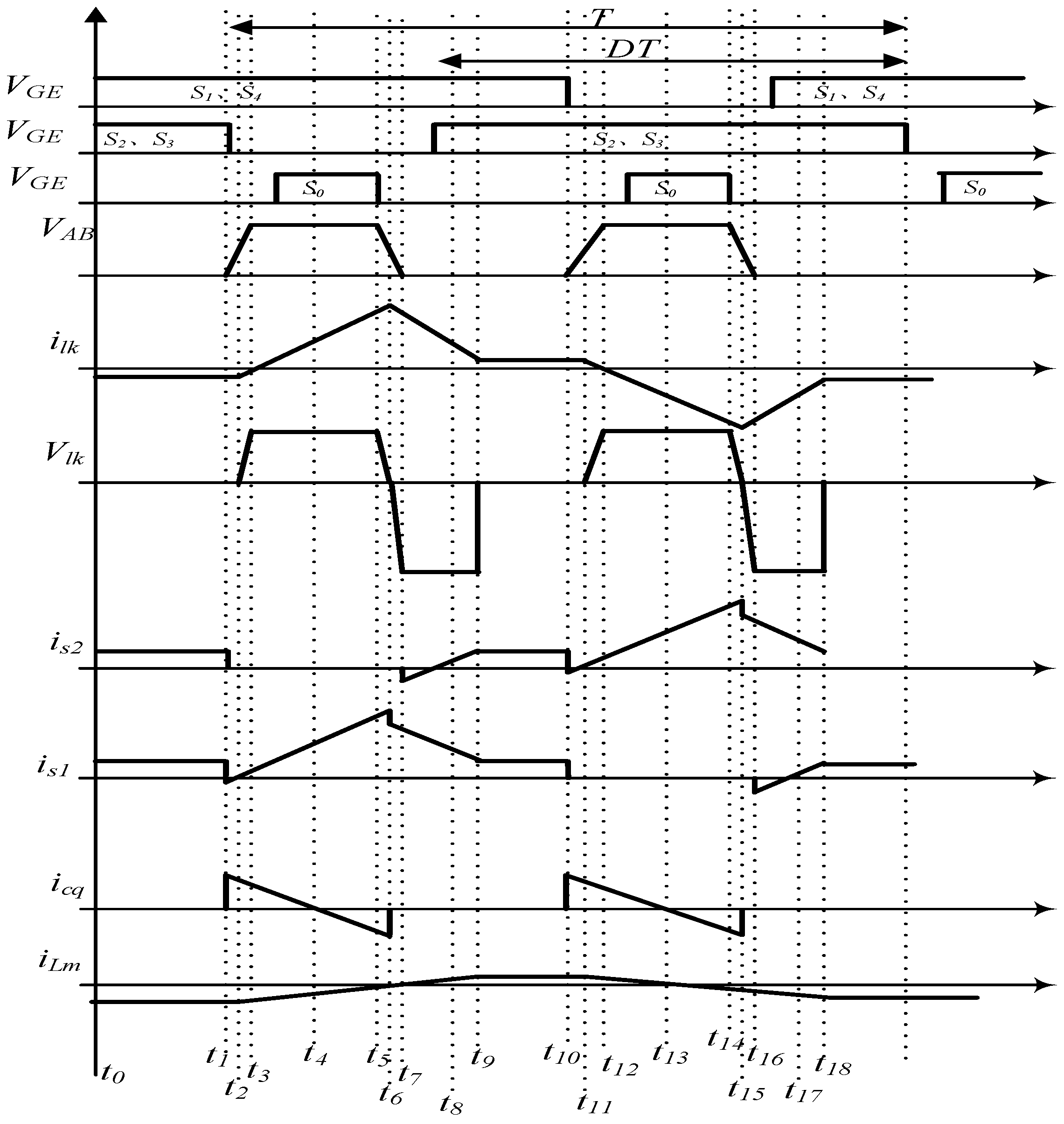
2.3. Analysis the Converter Operation Mode with Soft Switching

To improve the conversion efficiency of the converter, the soft switching strategy is proposed, and the constraint conditions of soft switching are derived in detail.
When the stored energy of the inductance is fed to the load side of the transformer through S1 and S4, the clamping capacitor is charged first and then discharged. If the active clamping switch S0 turns off before the H-bridge switches S2 and S3 turn on with t, due to the freewheeling effect of the leakage inductance of the transformer, the leakage inductance current remains unchanged at the moment of S0 turn off, and the leakage inductance of the transformer resonates with the junction capacitors of the switches S0, S2 and S3, causing C2 and C3 to be discharged. When the voltages of C2 and C3 reach zero, the anti-parallel diodes Ds2 and Ds3 turn on, and S2 and S3 have the condition of zero voltage turn on.
Soft switching analysis considering the excitation inductance of the transformer and switch junction capacitance is illustrated as follows. The operation mode timing sequence is shown in Figure 5, and it contains eighteen operation modes in the half switching period.
  • Operation mode I:
When t0 < t < t1, all four switches of H-bridge turn on, and the exciting inductor current realizes freewheeling through leakage inductance. At this moment, the active clamping capacitor switch is closed. The voltage of active clamping capacitor and active clamping switch are same. The value of leakage current shows as follows:
i l k = i m = I m p
where i l k is the leakage inductance current of the transformer, i m is the value of secondary exciting current converted to the primary side, I m p is the peak value of the exciting current, and it can be white as follows:
I m p = V i n 2 f ( L l k + L m )
The active clamping capacitor voltage is:
V c = V i n 2 ( 1 D )
The junction capacitor voltage of the clamping switch is:
V o = V c = V i n 2 ( 1 D )
  • Operation mode 2:
When t1 < t < t2, at t = t1, switches S2 and S3 are turned off, and the inductive current flows to the clamping capacitor, resulting in the H-bridge switches current being zero. The exciting current flows to the anti-parallel diodes DS1 and DS4 of the H-bridge switches S1 and S4 through the leakage inductance of the transformer, and then the current of the switches S1 and S4 changes from a positive value to a negative value, which is equal to the peak value of the exciting inductance current. The junction capacitors C2 and C3 of H-bridge switches S2 and S3 start to charge, and the junction capacitor of the clamping switch starts to discharge. In the secondary side, the rectifier diode is reversed, and the power is fed to the power grid by the output capacitor. When the junction capacitor voltage reaches the value of secondary side voltage converted to the primary side Vo/n, the operation mode finished.
  • Operation mode 3:
When t2 < t < t3, the junction capacitor voltage exceeds the secondary side reflection voltage Vo/N, the leakage inductance voltage of the transformer is (VinVo/n), the leakage inductance current begins to rise linearly, and the output voltage Vo appears on the secondary side excitation inductor. Moreover, the current increases linearly, and the rectifier diode begins to bias and conduct. The leakage inductor current is as follows:
i l k = I m p + V s 2 ( V o / n ) L l k ( t t 2 )
The exciting inductor current of the transformer is:
i m = I m p + V o L m ( t t 2 )
The current flows through H-bridge switch S1 can be written as:
i s 1 = I i 2 I m p + V s 2 ( V o / n ) L l k ( t t 2 )
At the end of this operation mode, the voltage of the clamping switch capacitor is discharged to zero. Junction capacitors C2 and C3 are charged to the maximum voltage, which is equal to the voltage of the clamping capacitor.
  • Operation mode 4:
When t3 < t < t4, the anti-parallel diode DS0 of clamping switch S0 starts to turn on, and the current flowing through it decreases rapidly. At this time, the switch S0 can be turn on to realize ZVS and reduce the turn-on losses. The leakage inductor current increases rapidly, and the current direction of switches S1 and S4 changes. The current flowing through the magnetizing inductance on the secondary side also increases with the same slope.
The leakage inductance current of the transformer is:
i l k = i l k ( t 3 ) + V c q ( V o / n ) L l k ( t t 3 )
The current that flows through the H-bridge switch S1 can be written as:
i S 1 = i S 1 ( t 3 ) + V c q ( V o / n ) L l k ( t t 3 )
The magnetizing inductance current im is:
i m = i m ( t 3 ) + V o L m ( t t 3 )
The active clamping capacitor current icq is:
i c q = I c q p e a k ( t 3 ) V c q ( V o / n ) L l k ( t t 3 )
  • Operation mode 5:
When t4 < t < t5, the clamping switch S0 achieves zero voltage turn off and the leakage inductance current IL continues to rise with the slope of operation mode 4. Meanwhile, the magnetizing inductance current also rises with the same slope, and the clamping capacitor begins to discharge. At this point:
i l k = I i n ( t 3 ) + V c p ( V o / n ) L l k ( t t 4 )
i S 1 = I i n + i c q
i c q = I i n i l k = V c q ( V o / n ) L l k ( t t 4 )
The peak current of the H-bridge switch S1 can be expressed as:
i S 1 p e a k = I i n I m p + V o f L l k ( 1 D )
  • Operation mode 6:
When t5 < t < t6, at t = t5, the clamp switch is turned off. The leakage current charges the junction capacitor C0 of the clamp switch and discharges the junction capacitors C2 and C3 of the H-bridge switches. The input inductance L resonates with the clamp capacitor C0, the junction capacitors C2 and C3 of the H-bridge switches. The angle frequency can be expressed as:
ω r = 1 L l k ( C 2 + C 3 + C 0 )
The junction capacitor voltage VS2 of the switch S2 is:
V s 2 = V c q V s 0
The voltage of clamping switch S0, the current of leakage inductance, and switch S1 can be written as:
V s 0 = I l k p e a k L l k C 2 + C 3 + C 0 sin ( ω r ( t t 5 ) )
i l k = I l k p e a k cos ( ω r ( t t 5 ) )
i S 1 = I S 1 p e a k cos ( ω r ( t t 5 ) )
When the operation mode 6 is finished, the voltages of the junction capacitor S2 and S3 are discharged to Vo/n, and the voltage of C0 is charged, the voltage of C0 and the voltage of switches S0 and S2 can be expressed as:
V C 0 = ( V c q V o / n )
V s 0 ( t 6 ) = V c q V o / n
V s 2 ( t 6 ) = V o / n
  • Operation mode 7:
When t6 < t < t7, the leakage inductance current is still charging the clamping capacitor and discharging the switch junction capacitor through the resonant process, and the leakage inductance current decreases slightly in this process. At the end of the process, the junction capacitor of the switch is discharged to zero and the resonant capacitor is charged to the initial value. Finally, VS2 = zero and VS0 = Vcq.
  • Operation mode 8:
When t7 < t < t8, the anti-parallel diodes DS2 and DS3 of the H-bridge switches turn-on respectively, and the switches S2 and S3 achieve ZVS. The leakage inductance current decreases with the slope (Vo/(nLlk)), and the leakage inductance current and the anti-parallel diode DS2 current can be written as follows.
i l k = I l k ( t 7 ) V o n L l k ( t t 7 )
i D s 2 = i l k I i n
When ilk = Iin, the operation mode 8 finished, and iD2(t6) = 0, ilk(t6) = Iin.
  • Operation mode 9:
When t8 < t < t9, the current of switch S2 and S3 begin to increase, while the leakage inductance current still decreases. The leakage inductance current is transferred to H-bridge switches S2 and S3. When the leakage inductance current decreases to the peak value of the magnetizing inductance current converted from the secondary side to the primary side current, the operation process is finished. The leakage inductance current and the H-bridge switch S2 current can be written as follows.
i l k = i S 2 = I i n V o n L l k ( t t 8 )
i S 2 = V o n L l k ( t t 8 )
Finally, at the time of t9, the H-bridge switches S2 and S1 current and the leakage inductance current can be written as follows.
i S 2 ( t 9 ) = I i n I m p
i S 1 ( t 9 ) = I i n + I m p
i l k ( t 9 ) = i L P ( t 9 ) = I m p
The rest of the operation mode analysis process is as shown above and will not be repeated.

2.4. Soft Switching Constraints for Wide Input Voltage Range

After the analysis in the previous section, when the converter works in operation mode 6, the energy stored in the leakage inductance of the transformer must meet the requirements of charging the capacitor for realizing the LC resonance process of soft switching. According to the voltage expression of switch S2:
V s 2 = V c q V s 0
V s 0 = ( I l k p e a k I L ) L l k C 2 + C 3 + C 0 sin ( ω r ( t t 5 ) )
The voltage of the switch S2 can be expressed as:
V s 2 = V c q ( I l k p e a k I L ) L l k C 2 + C 3 + C 0 sin ( ω r ( t ) )
Before S2 is turned on, the voltage Vs2 meets the condition of being less than or equal to zero, i.e., the ZVS condition of switch S2 is satisfied:
V c q I l k p e a k L l k C 2 + C 3 + C 0 sin ( ω r ( t ) ) 0
The resonance condition shows as follows:
sin ( ω r ( t ) ) = 1
V c q = V i n 2 ( 1 D )
It can be deduced that:
V i n 2 ( 1 D ) ( I l k p e a k I L ) L l k C 2 + C 3 + C 0
After simplification, the requirement of leakage inductance to realize the ZVS can be obtained as follows:
L l k ( V i n 2 ( 1 D ) ( I l k p e a k I L ) ) 2 ( C 2 + C 3 + C 0 )
According to the resonance condition, the resonance period is obtained as follows:
T = 2 π L l k ( C 0 + C 2 + C 3 )
Then, the conduction time difference between active clamping switch and H-bridge switches should meet the following requirements:
Δ t 2 π L l k ( C 0 + C 2 + C 3 ) 4 = π L l k ( C 0 + C 2 + C 3 ) 2

3. DC/DC Converter Control Strategy

This section analyzes the control strategy of IPOS module cascaded PV high voltage DC/DC grid-connected converter. It consists of the basic control strategy such as MPPT control, power limiting control, and the input current and output voltage equalization control strategy.

3.1. Basic Control Strategy of the Converter

In PV HVDC collection and grid-connection application occasion, the DC/DC converter mainly realizes the maximum power point tracking (MPPT) function of PV array. The basic control strategy of the converter is to calculate the input voltage reference command through the MPPT algorithm according to the output voltage and current of the PV array, and then realize the double closed-loop control by the input voltage closed-loop and output current closed-loop. The grid-connected power can be controlled by controlling the output grid-connected current of the DC/DC converter. In addition, the converter needs to have the function of response the power dispatching command of the PV power plant. When receiving the power dispatching command of the PV power plant, the PV DC/DC converter must control its output power according to the power dispatching command and the current real-time output power. When the PV power plant receives the power grid power limiting dispatching command, if the current output power of the converter is less than the power limiting dispatching command value, the DC/DC converter will operate in the maximum power point tracking mode according to the current actual output power. If the current output power of the converter is greater than the power limiting dispatching command value, the converter will operate according to the power limiting command and, deviating from the maximum power point tracking mode, execute the power limiting operation mode. The basic control strategy of PV DC/DC converter is shown in Figure 6.

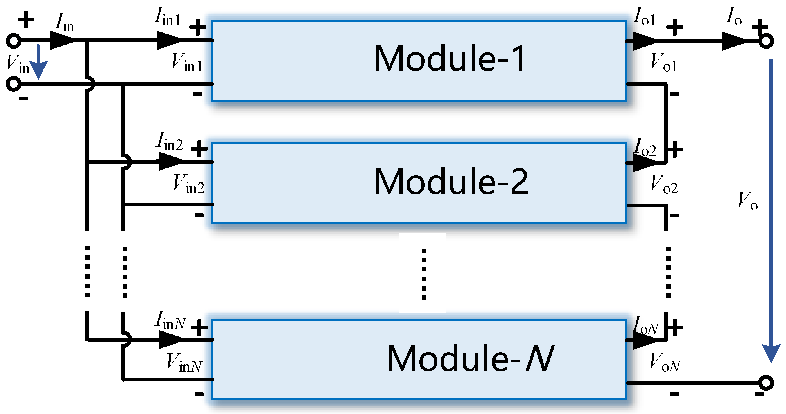
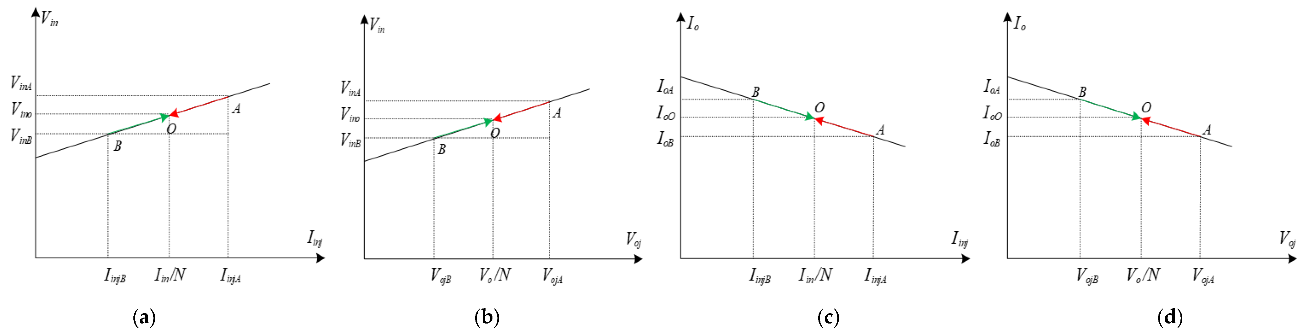
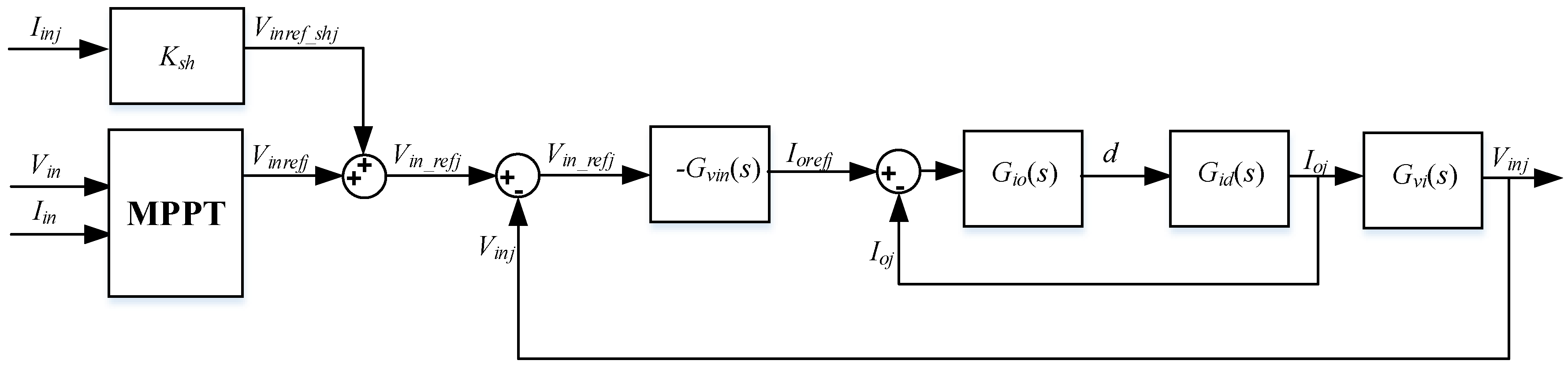
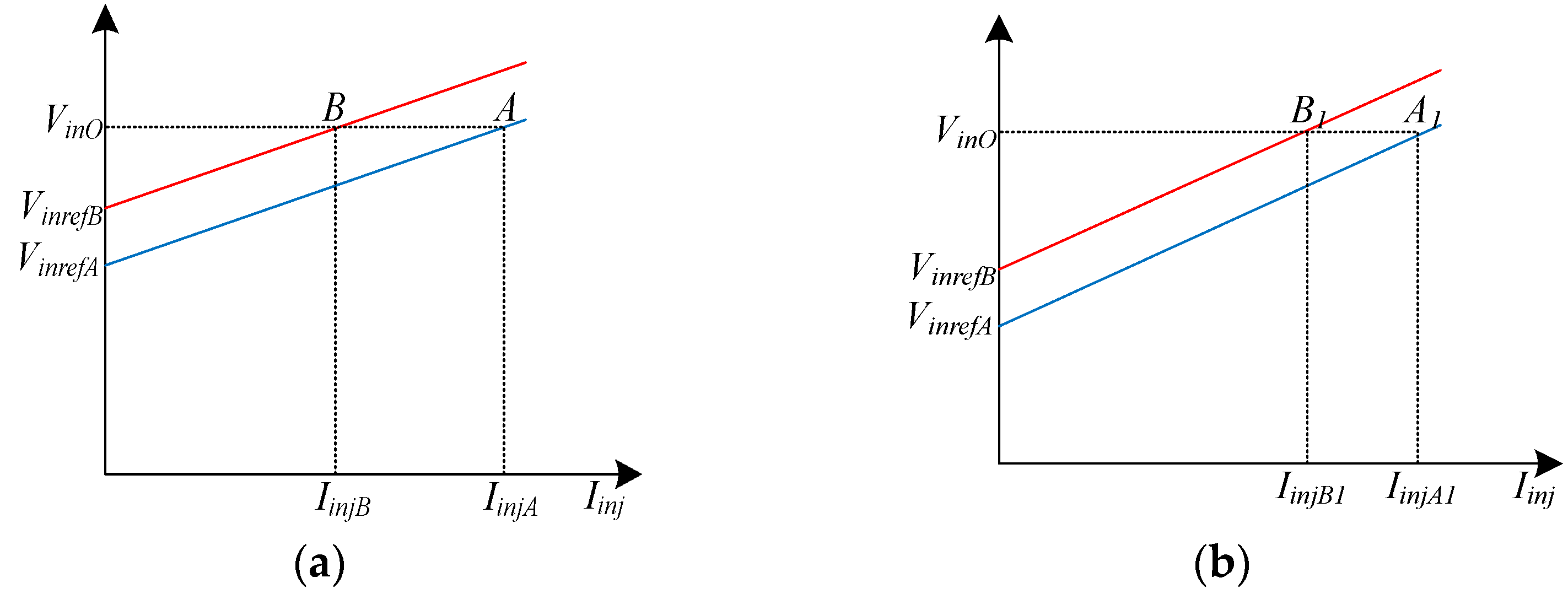
3.2. Input Current and Output Voltage Equalization Control Strategy

The PV HVDC grid-connected DC/DC converter adopts multi-modules input parallel output series structure, so it is necessary to control the input current sharing and output voltage sharing of power modules to ensure the normal operation of modules and the system. A multi-module cascaded IPOS converter is shown in Figure 7.
{ P 1 = V in 1 I in 1 = V o 1 I o 1 P 2 = V in 2 I in 2 = V o 2 I o 2 P N = V in N I in N = V o N I o N
where Vin1, Vin2, Vin3VinN are the input voltage of the IPOS modules, and Iin1, Iin2, Iin3IinN are the input current of the IPOS modules. Vo1, Vo2, Vo3VoN are the output voltage of the IPOS modules, and Io1, Io2, Io3IoN are the output current of the IPOS modules. P1, P2, P3, PN are the output power of the IPOS modules, respectively.
Meanwhile, the modules have the same input voltage and the same output current because of the modules cascaded with IPOS structure.
{ V in 1 = V in 2 = ...... = V in N = V in I o 1 = I o 2 = ...... = I o N = I o
From the Equations (43) and (44), it can be deduced the Equation (45):
{ V o 1 = V o 2 = ...... = V o M P 1 = P 2 = ...... = P M I in 1 = I in 2 = ...... = I in M
From the analysis above, it can be concluded that in the module cascaded IPOS structure, in the steady state, the output voltage can be balanced as long as the input current is balanced, and vice versa. From the point of view of implementation, the input current balancing control has lower cost and easier implementation. To realize the imbalance of module input current and output voltage caused by inconsistent parameters between modules, a distributed module equalization control strategy is proposed to ensure the normal operation of power module and converter. In the IPOS structure, when the input current of a module is high, its output power should be reduced, so as to reduce the input current. In the double closed-loop control of DC/DC converters, increasing the input voltage will reduce the output current, and then reduce the input current. Therefore, when the module input current is too large, the module input current can be reduced by increasing the input voltage command. By introducing the input current into the input voltage command as a current equalization command, the input current sharing control between modules can be realized, as shown in Figure 8a.
The input voltage command of the module has a linear relationship with the input current, and the input voltage command directly reflects the balance of the input current, since the input voltage of each module is the same, the input current is basically the same after stabilization. By introducing the output voltage as the equalization command into the input voltage command, the relationship between the module input voltage and the output voltage can be derived, as shown in Figure 8b. Similarly, the relationship between module output current, input current and output voltage can be deduced, as shown in Figure 8c,d.
Taking Figure 8a as an example, the working process of the distributed equalization control strategy is analyzed. Point O in the Figure is the average input current Iin/N. When the module operates at point A, the input current is IinjA. At this time, through increasing the input voltage command of the power module, the output current of the module decreases, and then the input current of the module decreases, and the module working point moves to point O. When the module operates at point B, the input current IinjB of the module is lower than the average current. At this time, through reducing the voltage command of the module, the module output current increases, the input current also increases, and the module operating point moves to point O. According to the characteristics of module input voltage and current, as well as the input parallel and output series connection relationship between modules, the module input current corresponds to the unique input voltage. Therefore, the distributed input current sharing control can be realized by adjusting the input voltage.
In Figure 8a,b, the module input voltage has a linear relationship with the input current or output voltage, and the slope is positive, which is equal to increasing the input impedance of the module to realize voltage and current sharing. The relationship between the module input voltage command and the input current or output voltage can be expressed as follows:
V i n _ r e f j = V i n r e f j + K s h I i n j
V i n _ r e f j = V i n r e f j + K s h V o j
where Vinrefj represents the original input voltage command of the jth module, Iinj represents input current of the jth module, Voj represents output voltage of the jth module, Ksh is the equilibrium control coefficient, and Vin_Refj represents actual input voltage command of the jth module.
In Figure 8c,d, the output current of the module has a linear relationship with the input current and output voltage, and the slope is negative. It is equivalent to increasing the output impedance of the module to realize voltage and current sharing. The relationship between module output current command, input current, and output voltage can be expressed as:
I o _ r e f j = I o r e f j K s h I i n j
I o _ r e f j = I o r e f j K s h v o j
where Iorefj represents original input voltage command of the jth module. Io_refj represents actual input voltage command of the jth module.
The four control strategies in Figure 8 are equivalent to each other. According to Figure 8a and Equation (46), the module control strategy based on distributed current sharing control strategy introduced into the input voltage loop can be obtained as shown in Figure 9, the equalization controller is the proportional link and Ksh is the equalization coefficient. Gvin is the input voltage closed-loop proportional-integral regulator, Gio is the output current closed-loop proportional-integral regulator, Gid is the transfer function between output current and duty cycle, and Gvi is the transfer function between output voltage and output current.
If the power module has completely consistent output voltage and current characteristics, the complete current sharing between modules can be realized. Due to the hardware differences between modules, the output characteristics of modules are inconsistent, i.e., the starting points of input voltage and input current characteristic curves are different, and the input current between modules is not completely balanced. The distributed module current sharing control characteristics based on the input current introduced into the input voltage closed loop control strategy are shown in Figure 10.
The starting point voltages of the two curves in Figure 10a are different. When the input voltage is VinO, the modules operates at point A and point B respectively, and the input currents are IinjA and IinjB respectively. Increase the slope of the characteristic curve, that is increasing the equalization coefficient Ksh, and the module operating points are A1 and B1 respectively, as shown in Figure 10b. Currently, the input currents are IinjA1 and IinjB1 respectively. By increasing the equalization coefficient Ksh, the imbalance of the input current is reduced. Therefore, in practice, the voltage and current equalization target can be met by selecting an appropriate equalization coefficient.

4. Test Results

To verify the proposed system structure and control strategy of the PV HVDC collection and grid-connection DC/DC converter, a 5 kV/80 kW standard power module is developed based on the boost full bridge isolated topology, and the experimental test of power module is completed. The ±30 kV/1 MW DC/DC converter engineering prototype is developed based on fourteen 5 kV/80 kW power modules. Finally, the ±30 kV/1 MW PV HVDC collection and grid-connection demonstration system has been constructed, and the performance and function of the DC/DC converter is tested.

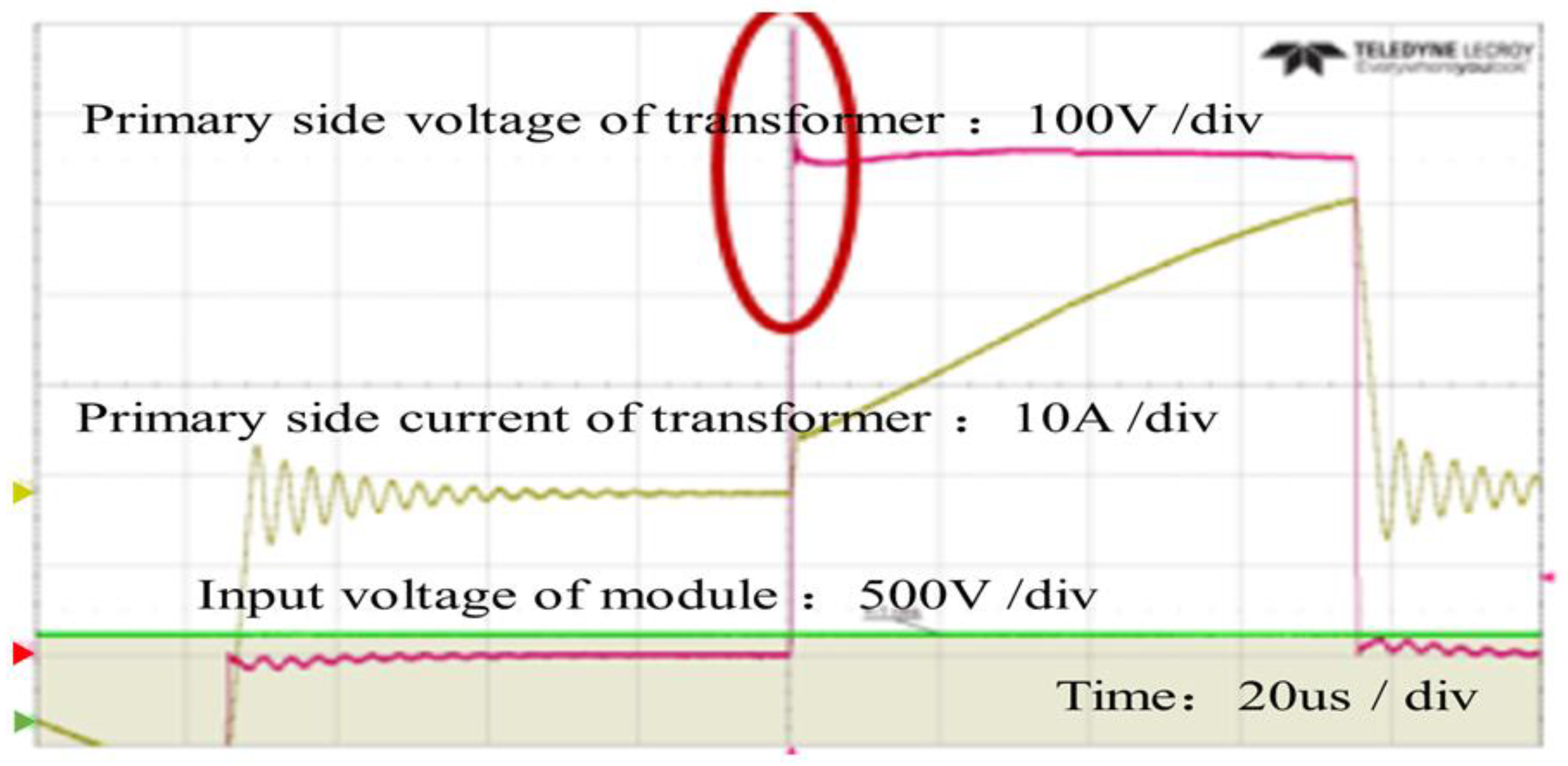
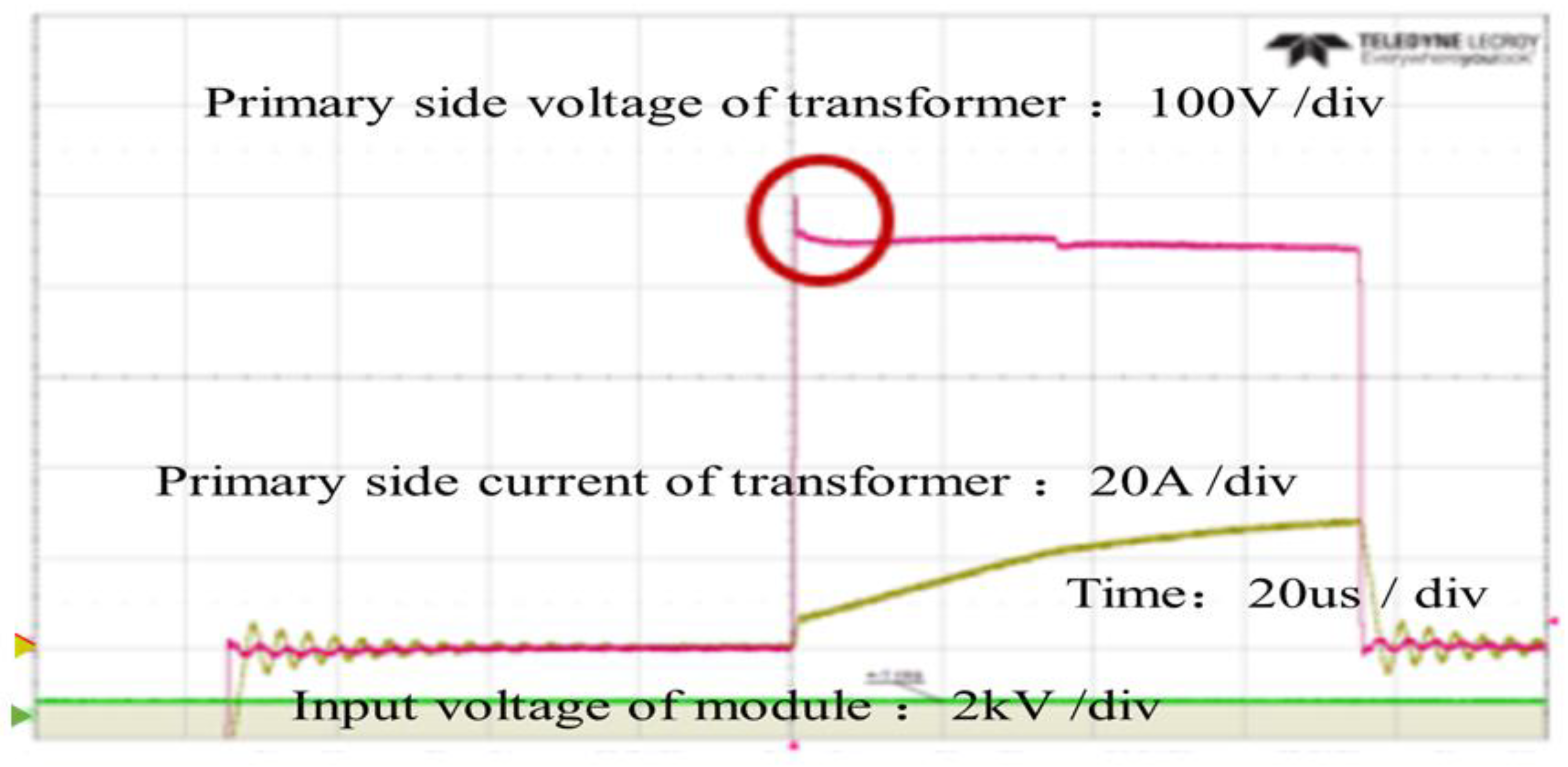
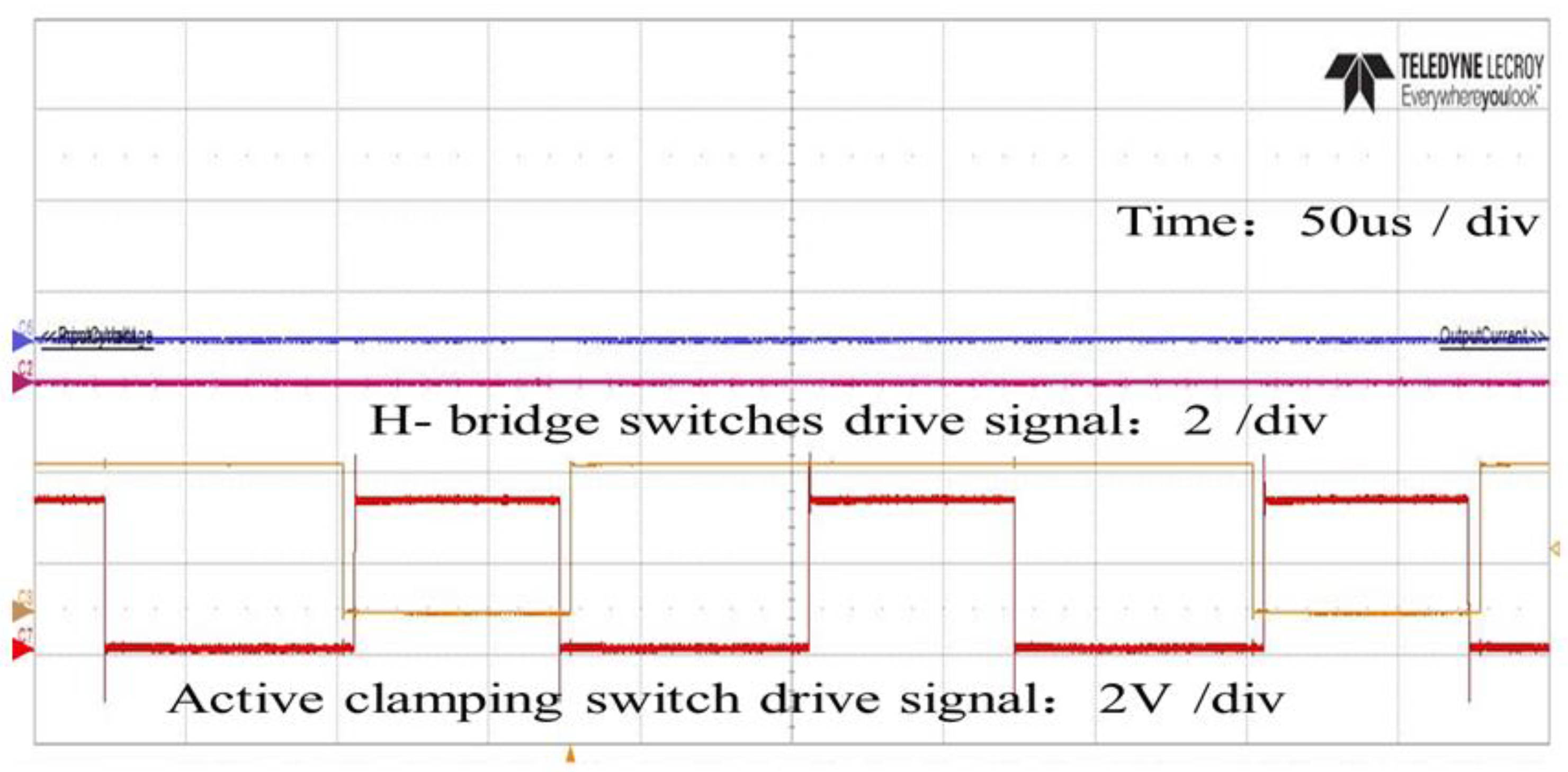
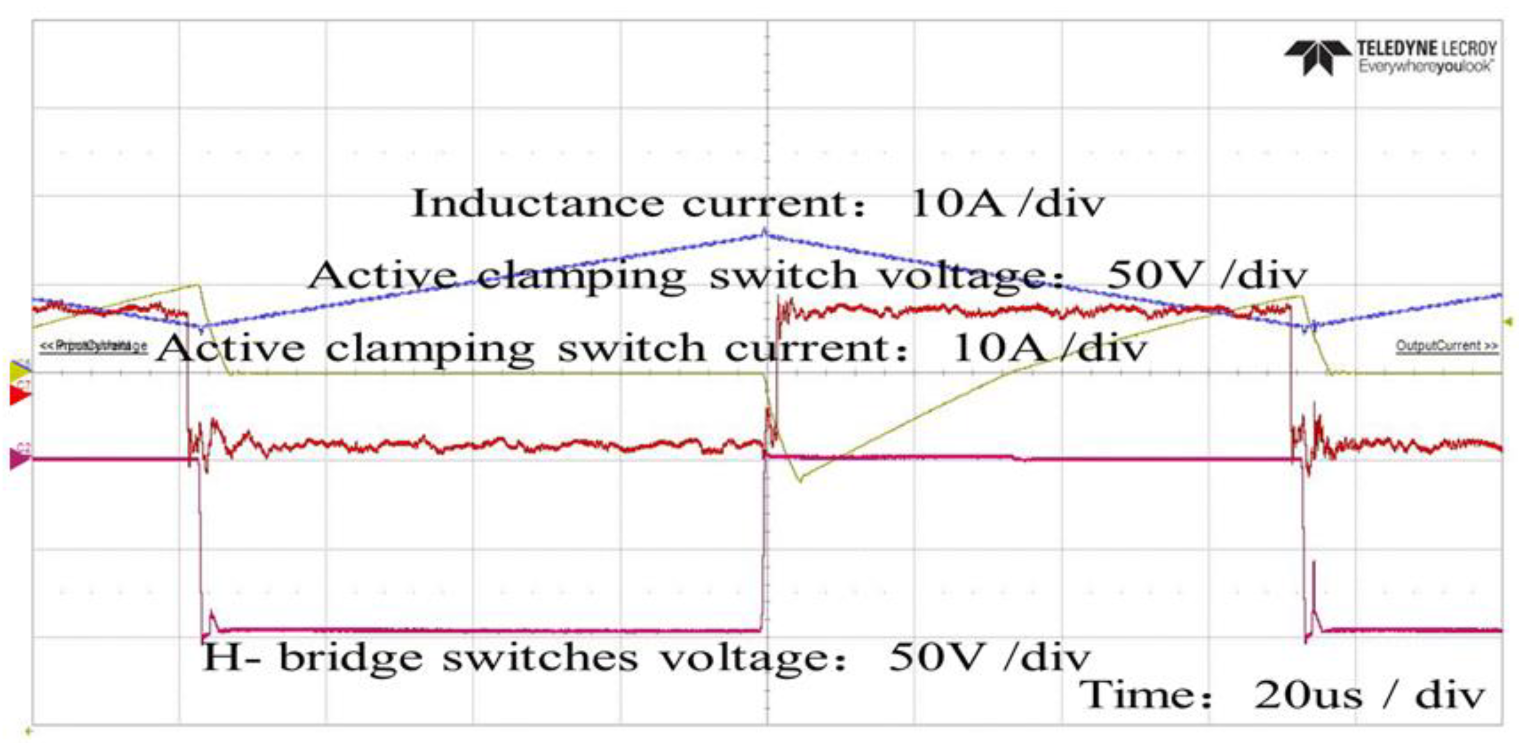
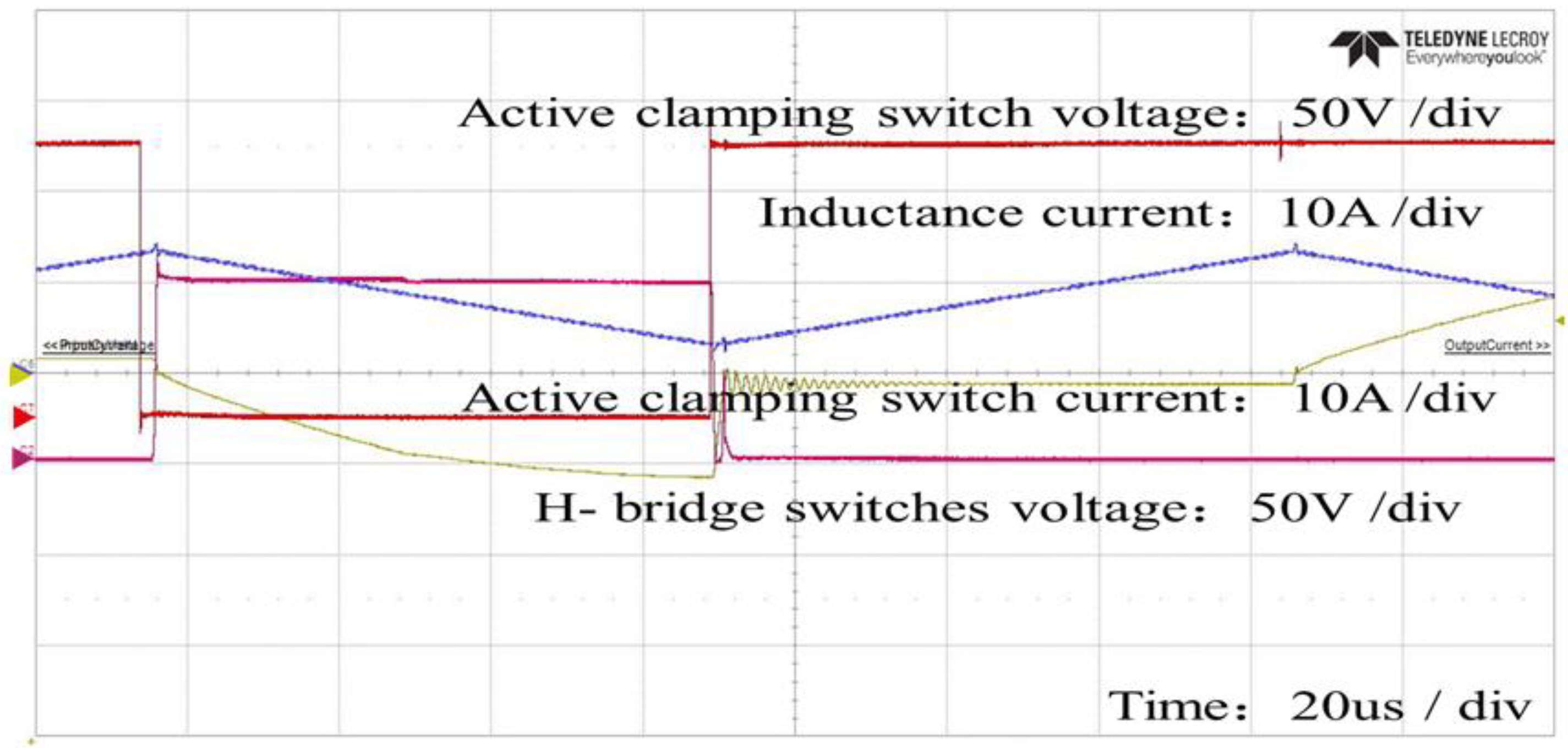
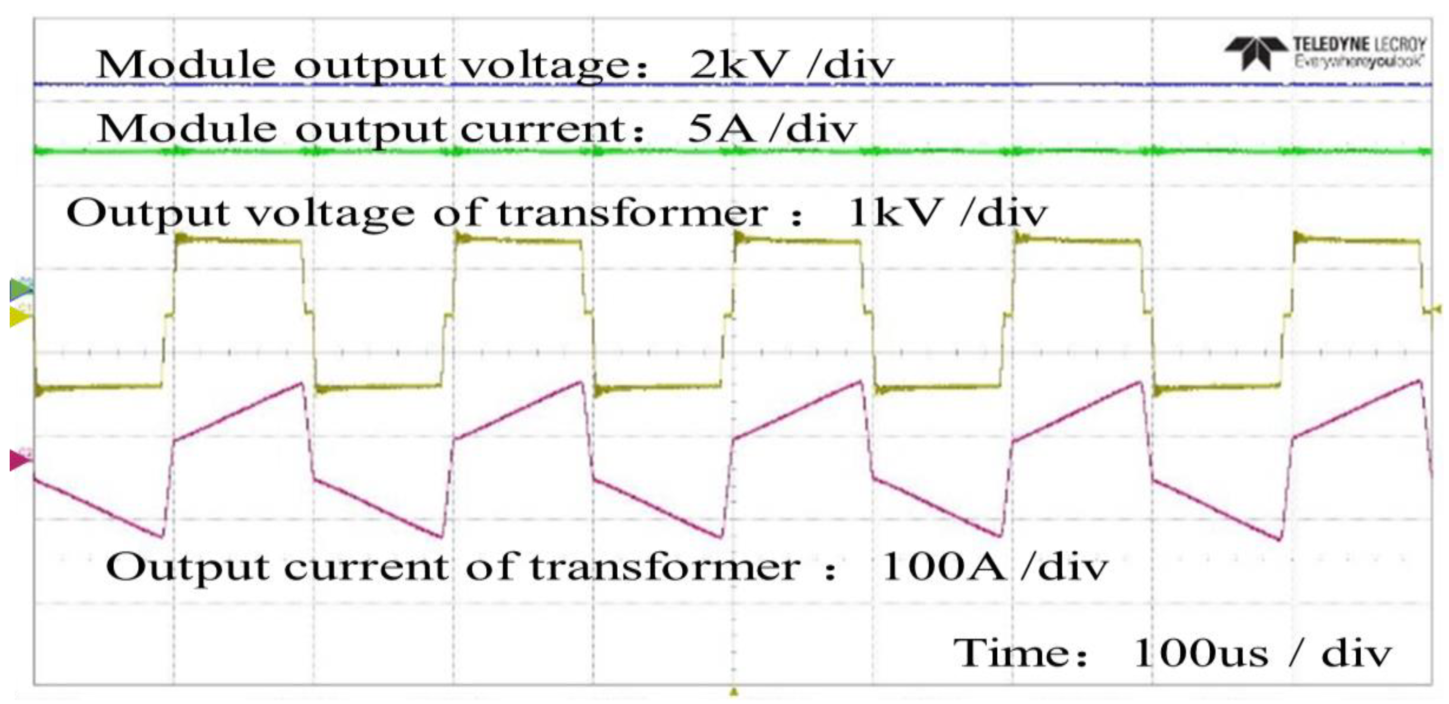
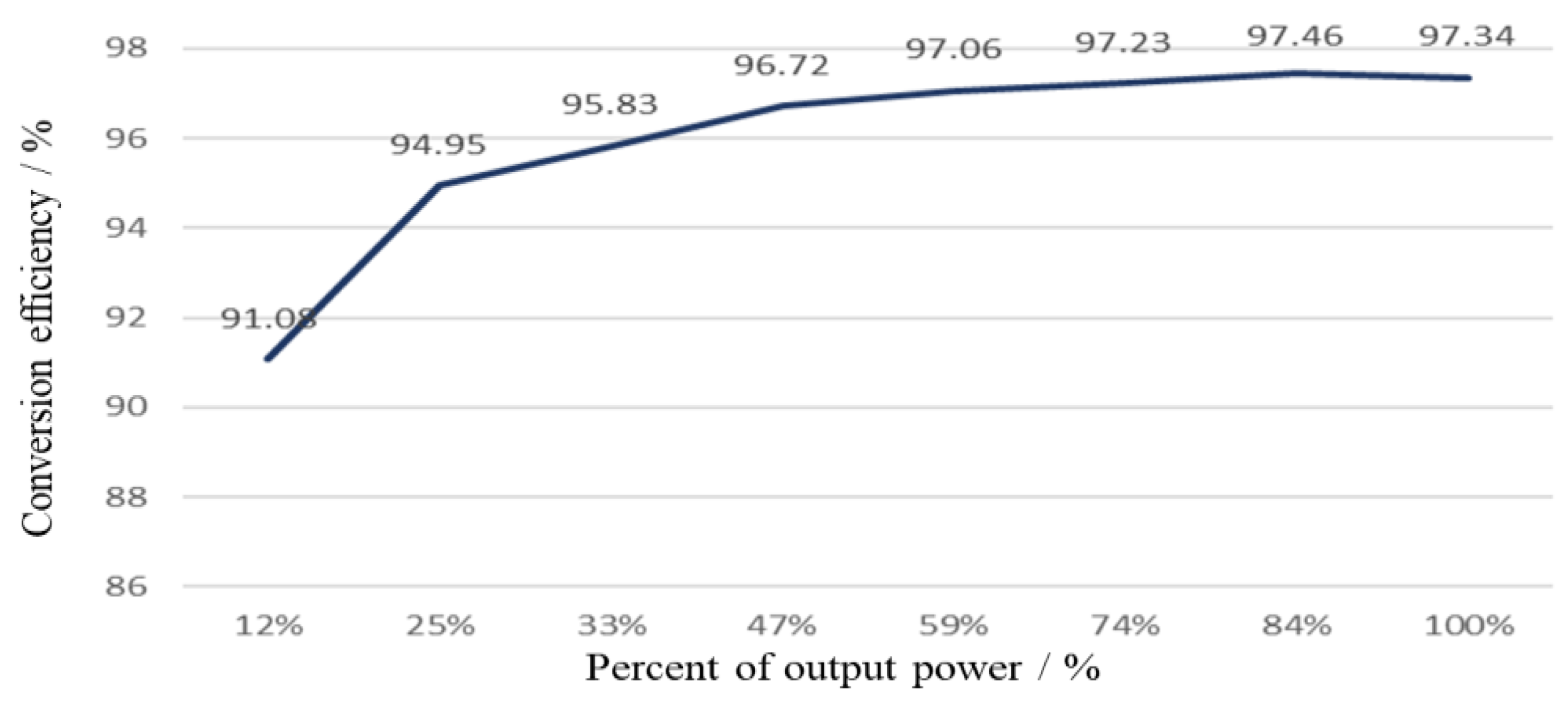
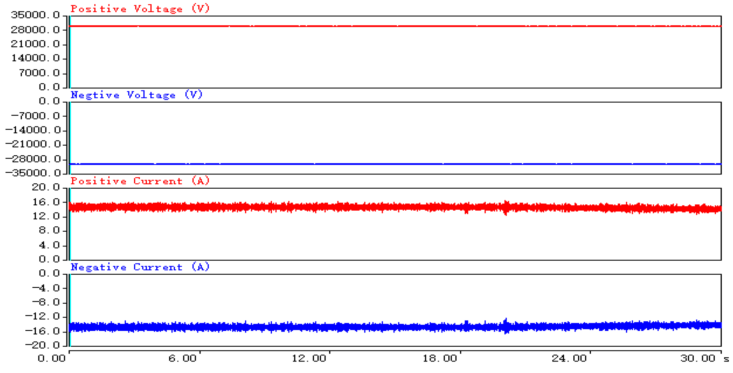
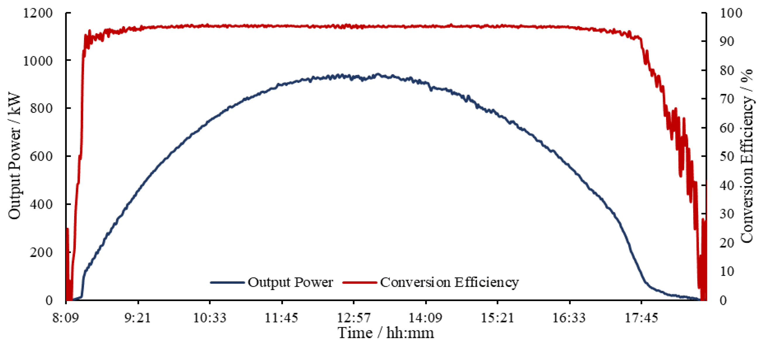
4.1. Experimental Verification of 5 kV/80 kW Power Module

The developed 5 kV/80 kW power module is shown in Figure 11. It is based on the boost full bridge isolated topology, which is mainly divided into three parts: low voltage module, high frequency transformer, and high voltage rectification module. The low voltage module realizes the first stage step-up voltage through the boost full bridge at the front end of the transformer. The high frequency transformer realizes the galvanic isolation of the converter and realizes secondary stage step-up voltage, and the high voltage rectifier module realizes the high frequency rectification of the output of the transformer. The three parts are combined to realize the low voltage PV to medium voltage power conversion.
As the most important part of the power module, on the one hand, the high frequency transformer is used to realize the function of voltage conversion with high step-up ratio. On the other hand, the high frequency transformer plays an important role in electrical isolation. Because the voltage of PV HVDC grid-connection system is ±30 kV, the high voltage side of the high frequency transformer needs to withstand the system voltage. Therefore, the insulation voltage level of the high frequency transformer needs to be designed according to the system voltage. At the same time, the voltage spike of the boost full bridge circuit switch is mainly caused by stray parameters such as transformer leakage inductance. Therefore, the leakage inductance of transformer must be minimized to reduce the voltage spike at the low voltage side of transformer.
The critical parameters of 5 kV/80 kW standard power module are shown in Table 1.
Figure 12 shows the voltage spike of the boost full bridge isolated power module without active clamping circuit when the H-bridge switches turn-off. The voltage spike of the H-bridge switches is up to 20% of the normal operation voltage value, which increases the voltage stress of the switches and affects the reliable operation of the converter.
Figure 13 shows the voltage spike suppression effect with active clamping circuit when the H-bridge switches turn-off. The voltage spike of the H-bridge switches can be effectively suppressed, and the voltage spike peak value can be controlled within 10% of the normal operation value.
Figure 14 shows the drive signals of the active clamping switch and H-bridge switches. The active clamping switch turns-on after the H-bridge switches turn-off, and the active clamping switch turns-off before the H-bridge switches turn-on.
Figure 15 shows the experimental results of the active clamping switch ZVS process. Through turning-off the active clamping switch before the H-bridge switches turn-on, the active clamping switch can realize ZVS.
Figure 16 shows the experimental results of the H-bridge switches ZVS process. By turning-off the active clamping switch for a period of time before the H-bridge switches turn-on, the H-bridge switches can realize ZVS turning-on process. The soft switching can effectively improve the efficiency of the converter.
The steady-state voltage and current of the 5 kV/80 kW power module connected to 5 kV DC grid are shown in Figure 17. The power module is stable in operation. The voltage spike at the primary side of the high frequency transformer is effectively suppressed through controlling the active clamp switch. The input voltage of the converter is 450 V, and the output voltage is 5000 V. The voltage gain of the power module can be reached to eleven times.
Figure 18 is the conversion efficiency curve of the proposed converter. It can be seen that the conversion efficiency of the power module can reach more than 91% at 20% output power, and more than 96% at 50% output power. The maximum conversion efficiency of the converter can reach 97.46% at 80% output power. In summary, the power module has a high efficiency in a wide input voltage range and the whole output power range.

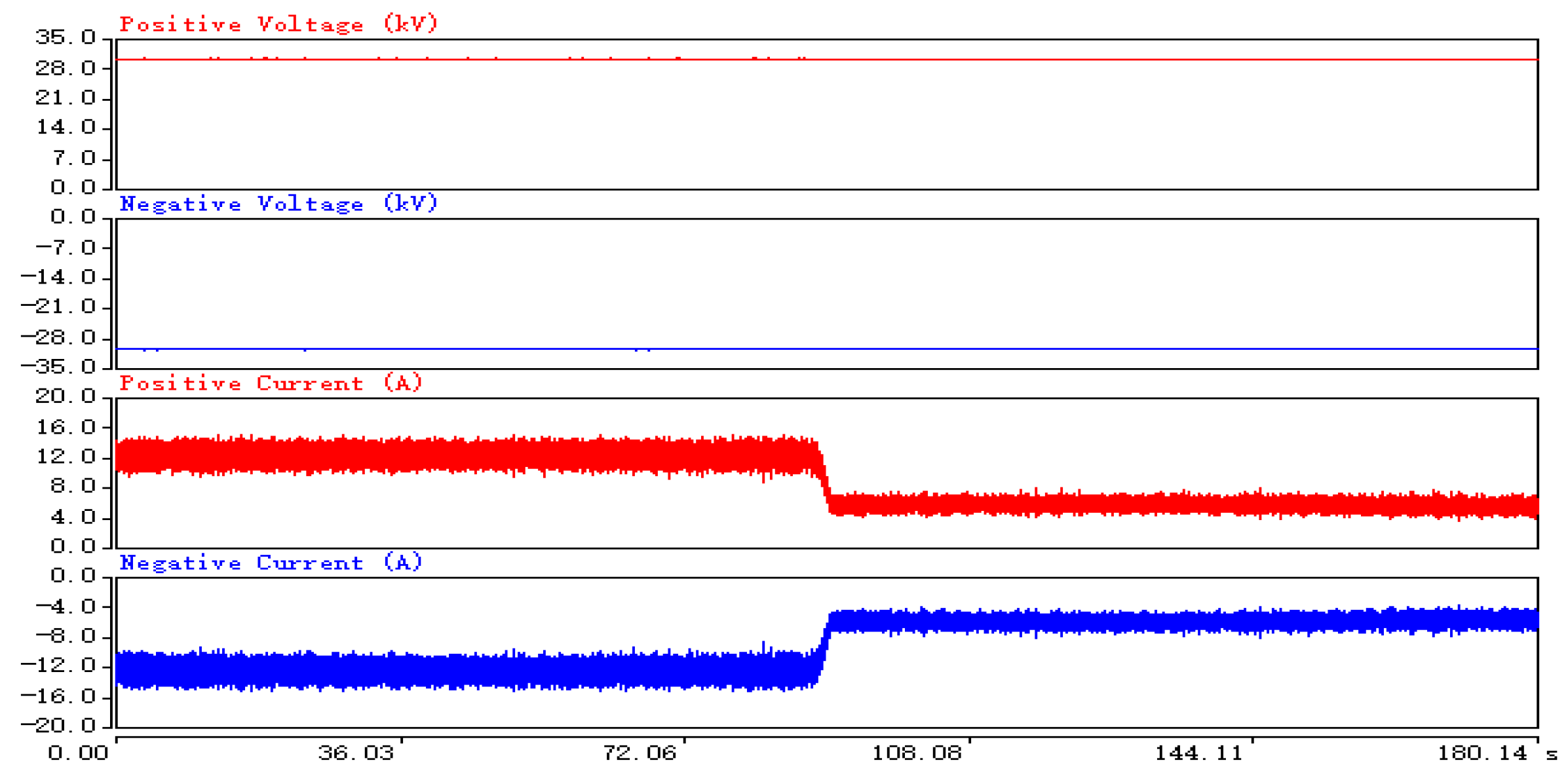
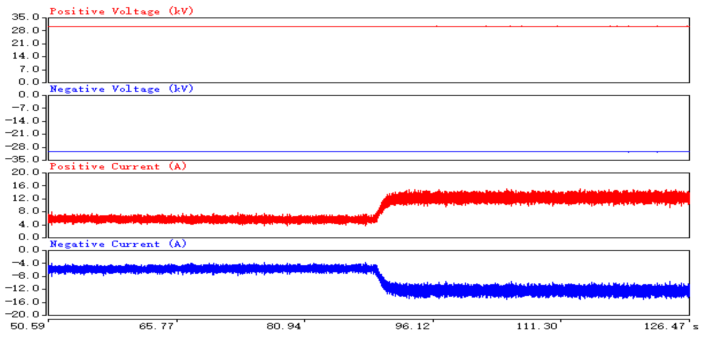
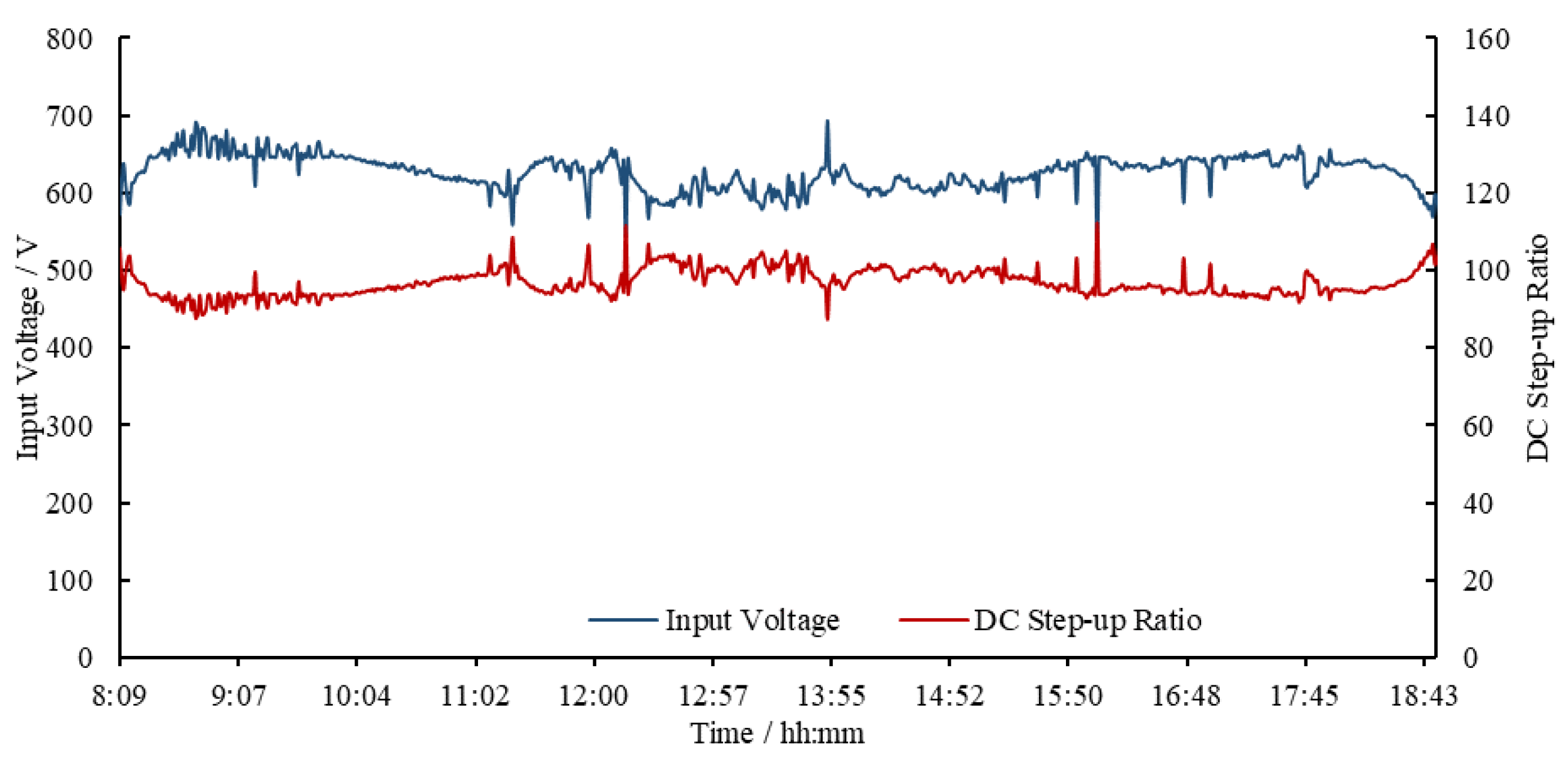
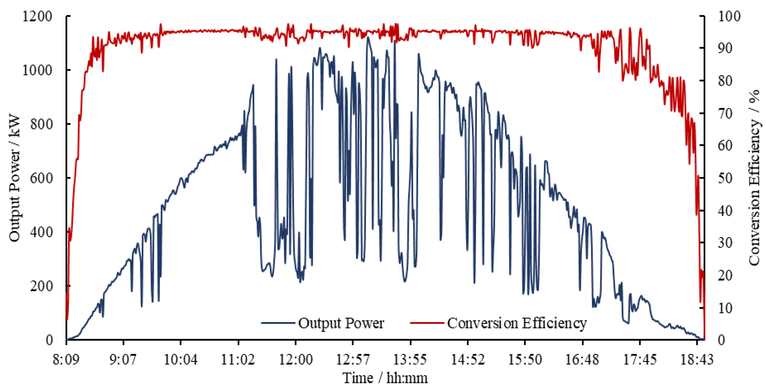
4.2. Experimental Verification of Multi-Module Cascaded DC/DC Converter

To verify the proposed distributed module equalization control strategy, an IPOS DC/DC converter experimental platform composed of two power modules is built, in which the transformer leakage inductance of module #1 is designed as 10 uH and the leakage inductance of module #2 is designed as 50 uH. The experimental platform is shown in Figure 19. The input of the converter connects to the PV simulator, and the output connects to the DC grid simulator.
Figure 20 shows the experimental waveform before and after the distributed module equalization control strategy is adopted for the DC/DC converter. When the distributed equalization control strategy is not adopted, the output voltage difference between module #1 and module #2 is about 200 V. After the distributed module equalization control strategy is added, module #1 and module #2 realizes the output voltage equalization, and the output voltage difference between the two modules reduces to 10 V.
Figure 21 shows the voltage equalization effect of the DC/DC converter modules when the equalization control coefficient is different. When the equalization coefficient is set as 0.05, the output voltage difference between the two modules is about 10 V. When the equalization coefficient is reduced to 0.0001, the output voltage difference between the two modules increases to 100 V. When the equalization coefficient is restored to 0.05, the voltage equalizing effect of the two modules is restored, and the output voltage difference between the two modules is reduced to 10 V.
Figure 22 shows the steady state operation waveform of the DC/DC converter composed of two modules using the distributed module equalization control strategy. The output voltage of module #1 and module #2 are equalized, and the two power modules and the converter reach the state of stable operation.

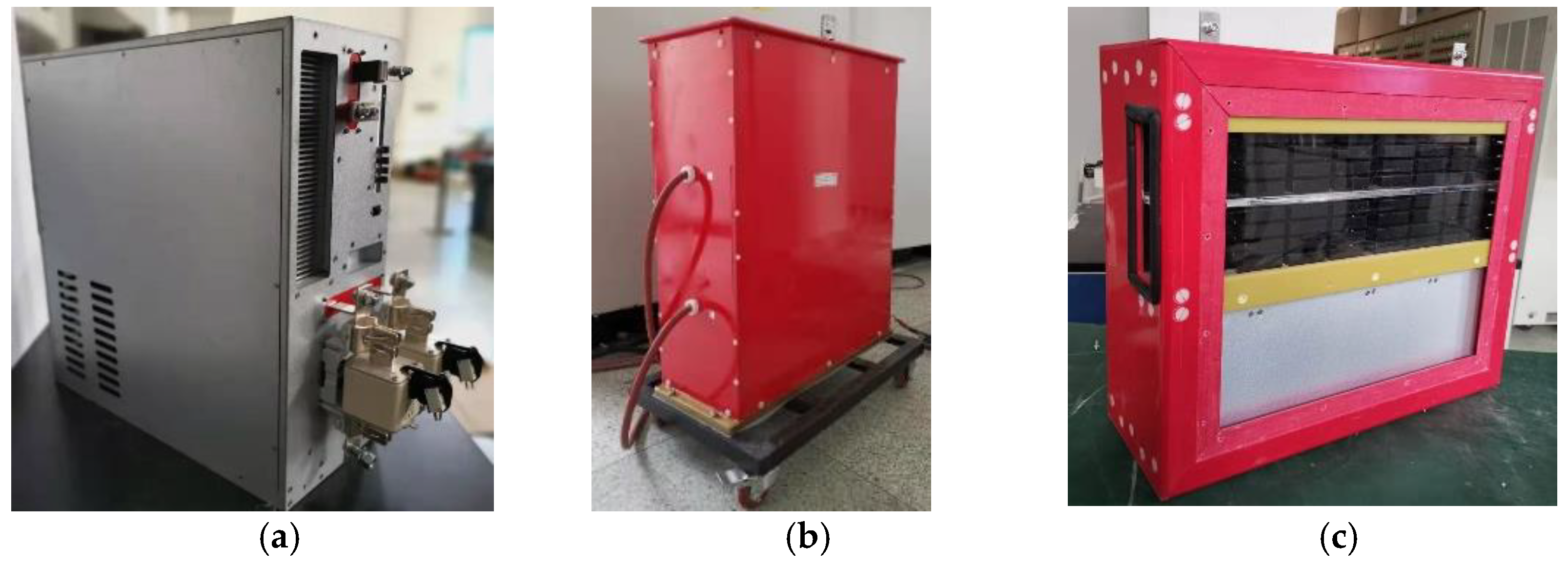
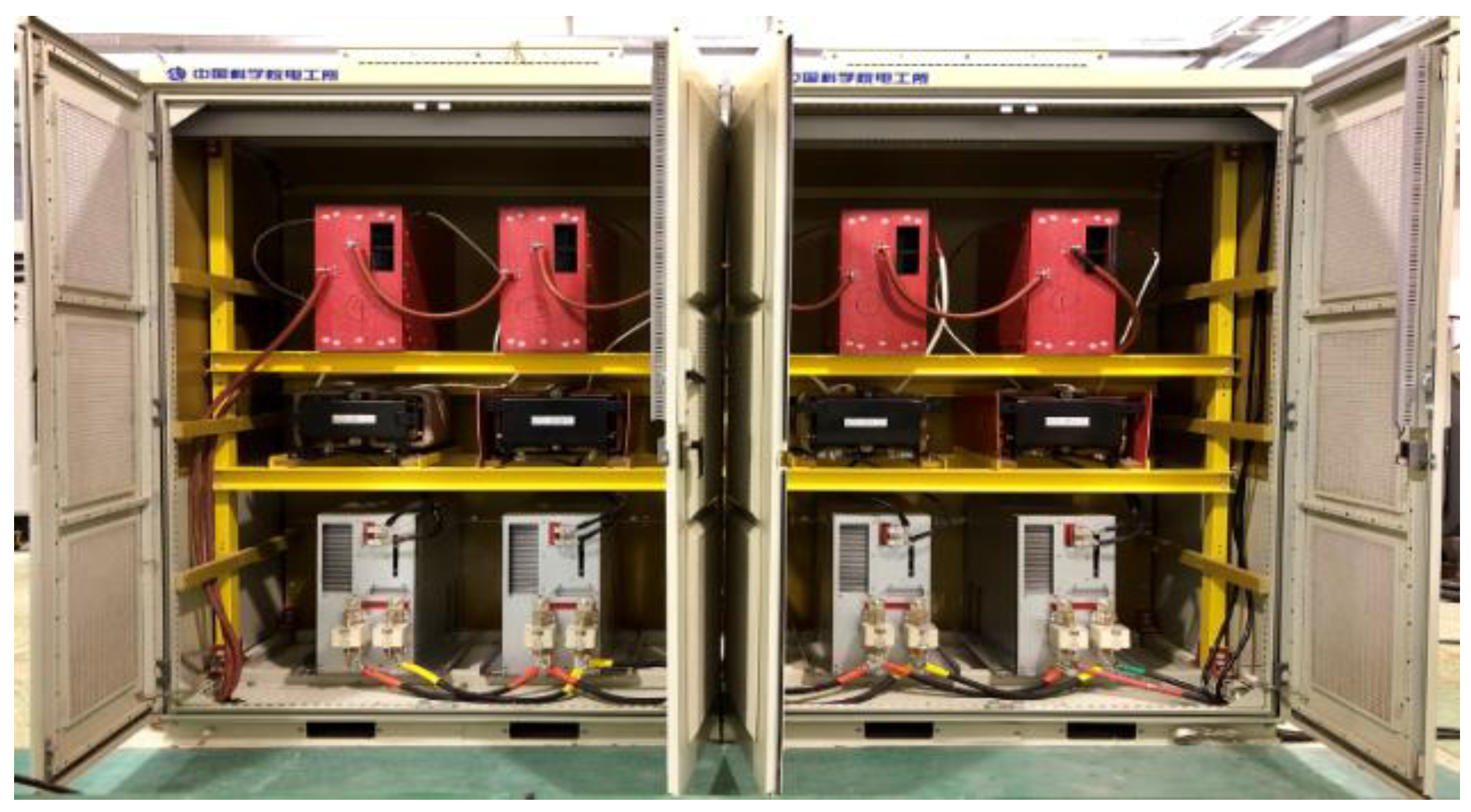
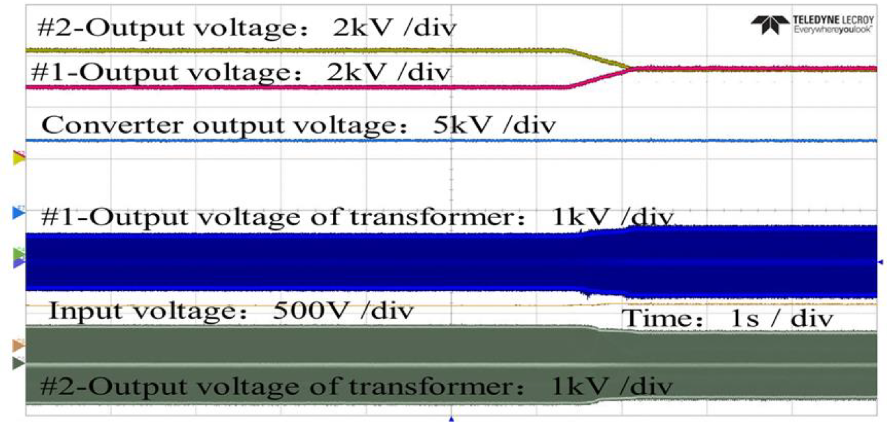
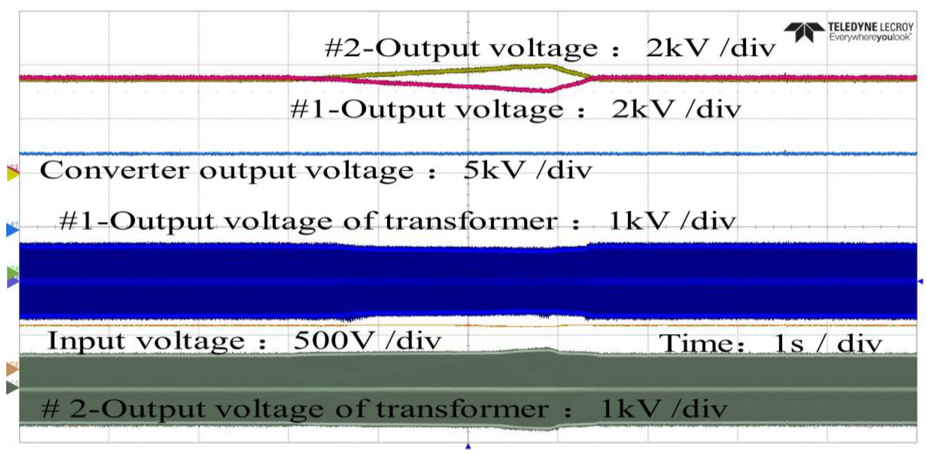
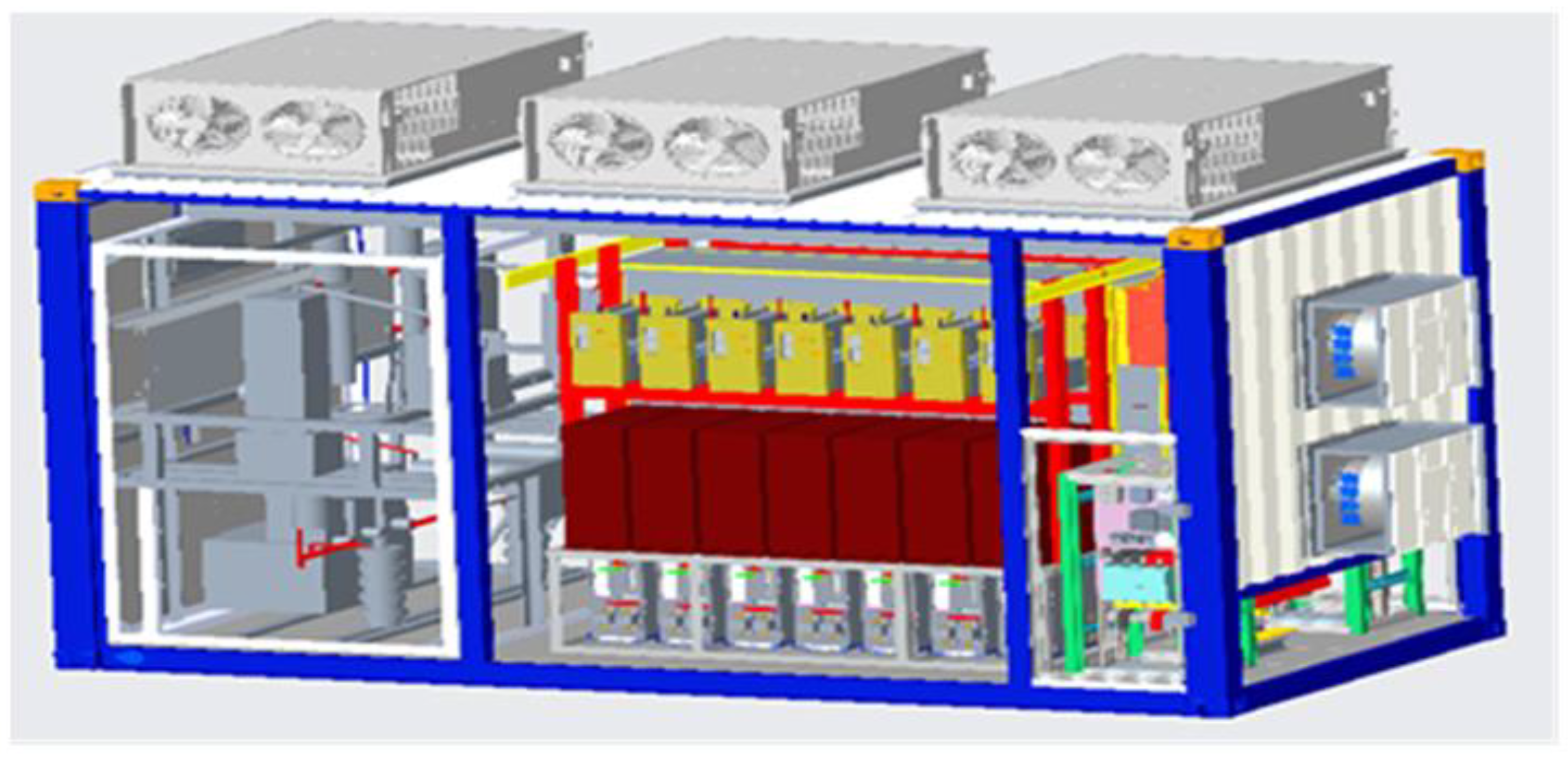
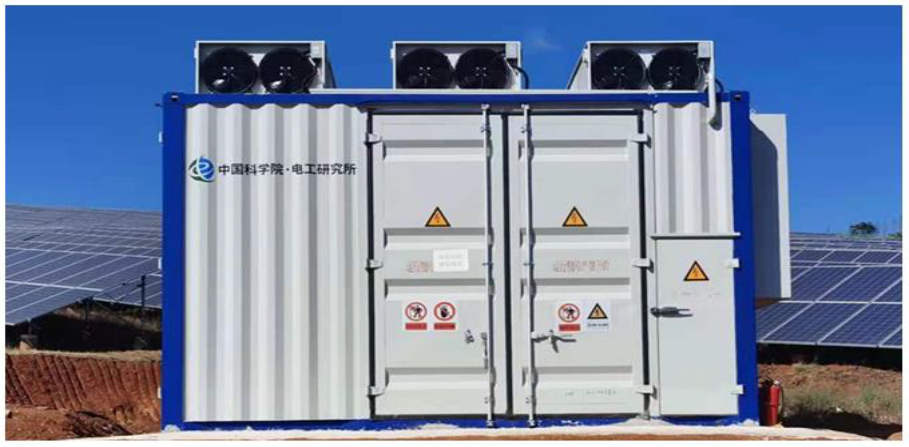
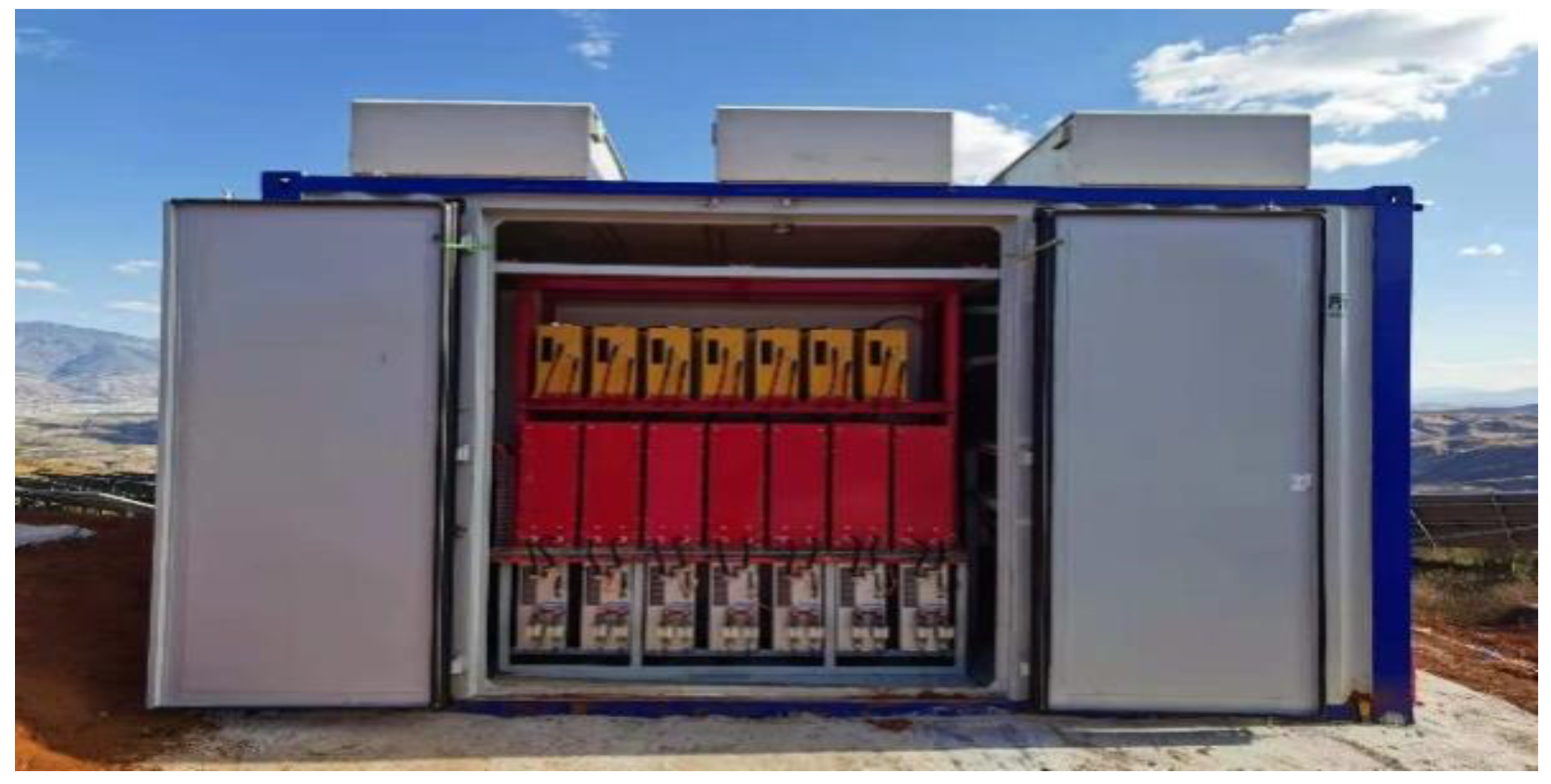
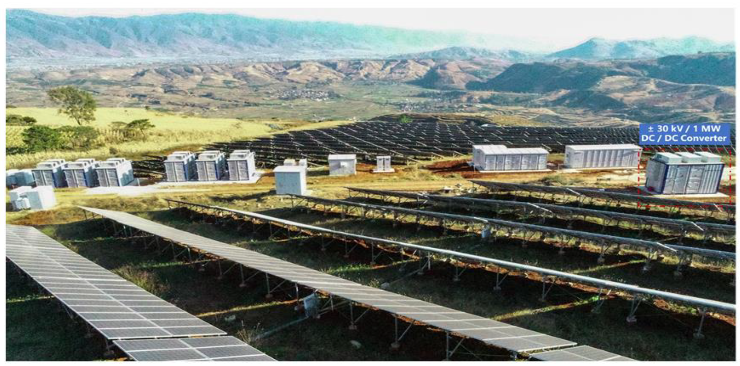
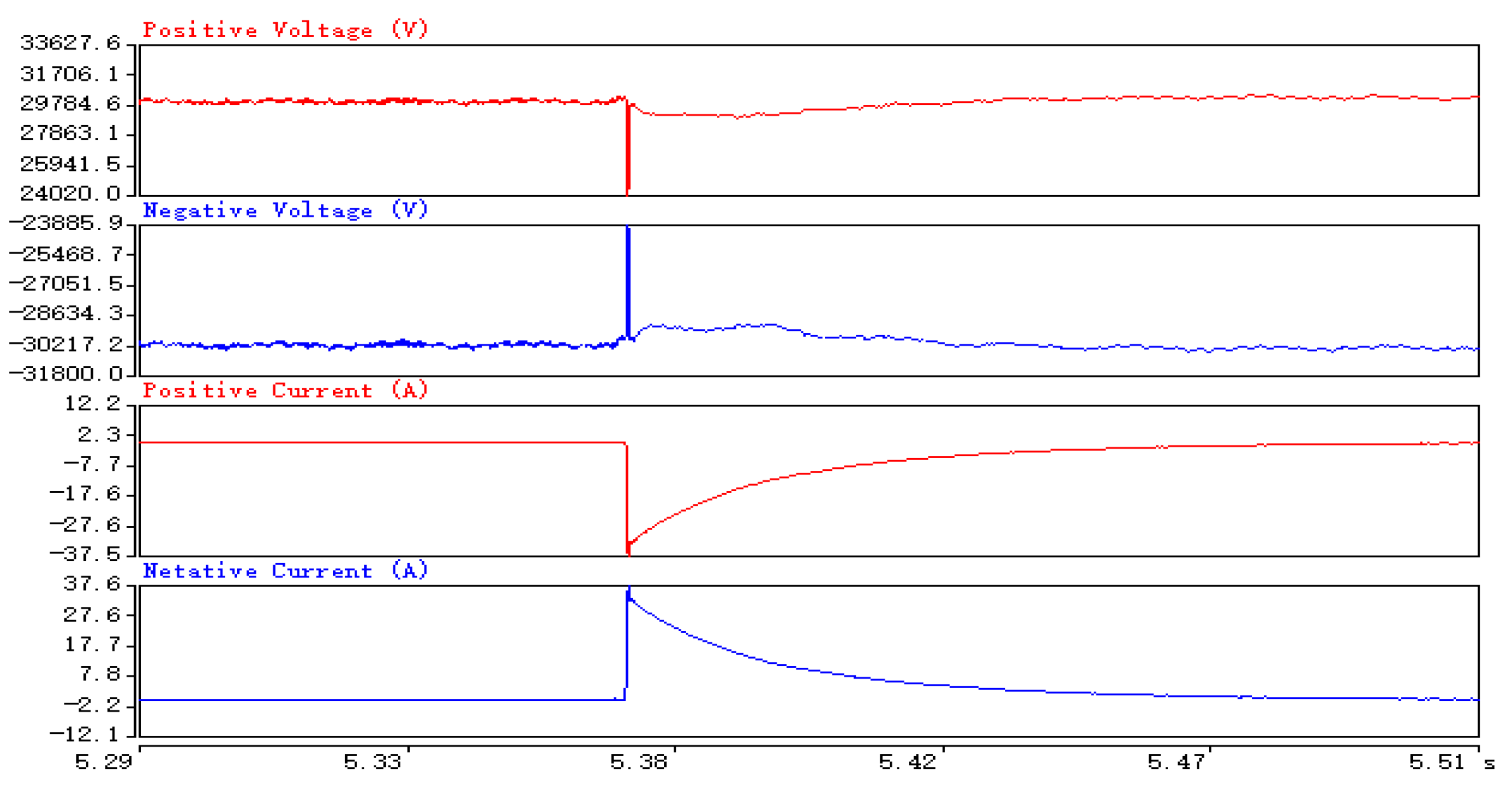
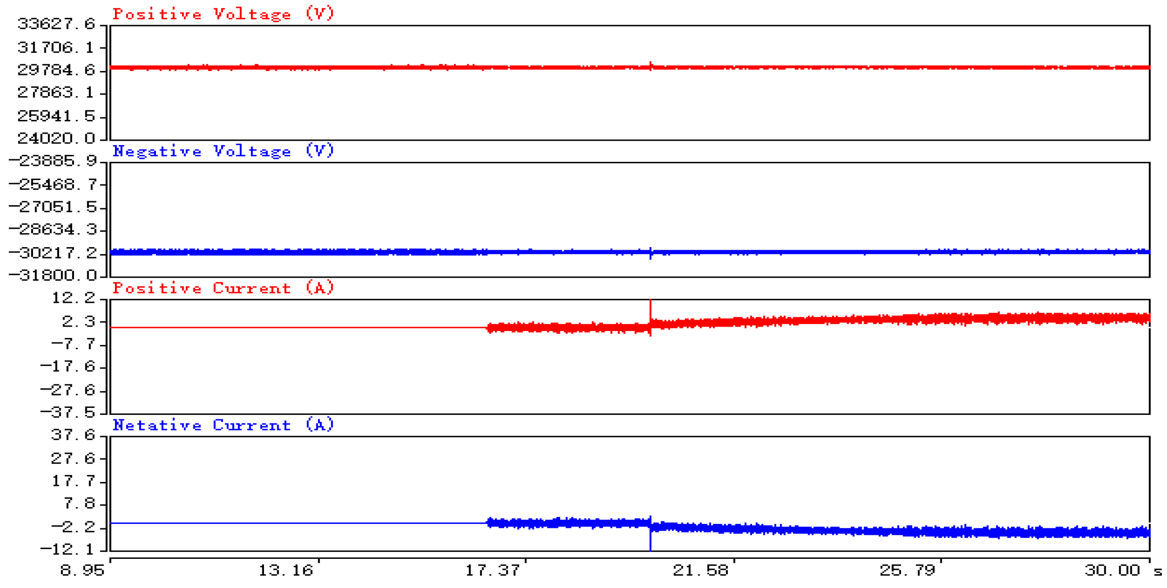
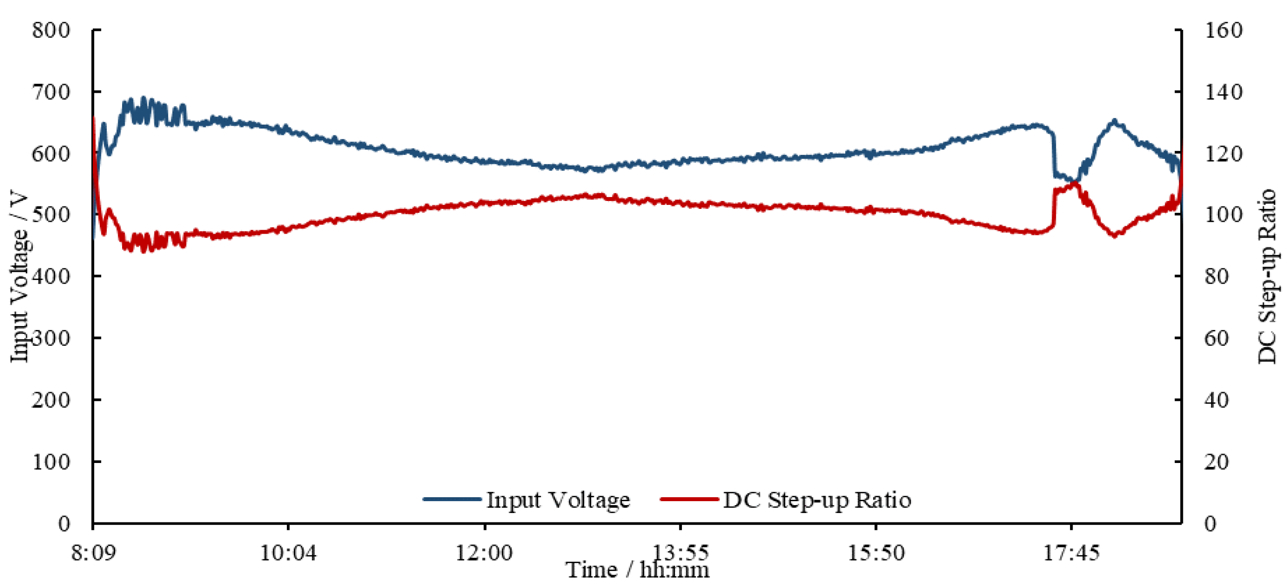
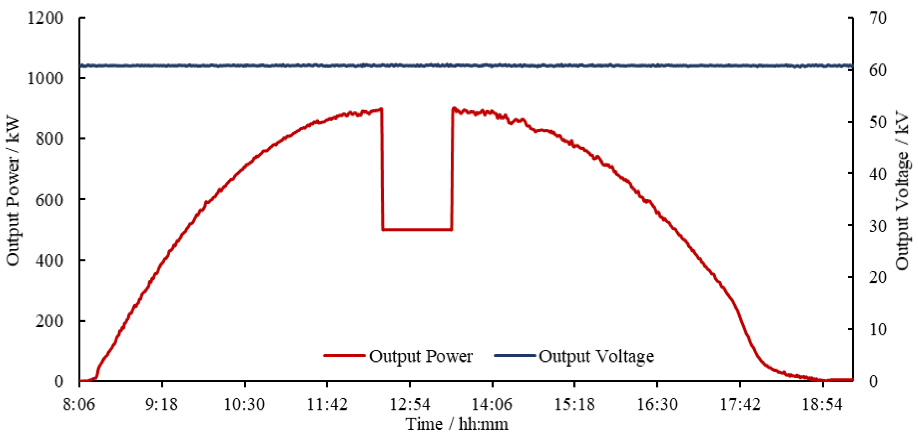
4.3. Demonstration System Verification of the ±30 kV/1 MW DC/DC Converter

A ±30 kV/1 MW DC/DC converter engineering prototype is developed based on fourteen 5 kV/80 kW power modules cascaded with input parallel and output series scheme. The converter includes twelve normal operation modules and two redundancy modules. Through setting up the redundant modules, the reliability of the converter can be effectively improved. A ±30 kV/1 MW PV power plant HVDC collection and grid-connection demonstration system is established, and the operation data of the DC/DC converter are obtained by the WDGL-VI/S microcomputer power fault recording and monitoring device.
The parameters of the ±30 kV/1 MW DC/DC converter engineering prototype are shown in Table 2.
Figure 23 shows the layout of the proposed ±30 kV/1 MW DC/DC converter. The left side of the converter is the high voltage switch cabinet, which consists of the contactor, soft start-up resistor, earthing knife-switch, and voltage and current measuring device. The middle part is power conversion cabinet of the converter, which consists of fourteen power modules and adopts a back-to-back layout structure. The right side is the low voltage part of the converter, which mainly consists of the controller of the converter.
Figure 24 shows the developed DC/DC converter engineering prototype that is applied to establish the ±30 kV/1 MW PV power plant HVDC collection and grid-connection demonstration system, and Figure 25 shows the inside of the DC/DC converter.
Figure 26 shows the ±30 kV MMC converter to build the ±30 kV high voltage DC bus for simulating the HVDC grid. Though the MMC converter, the DC/DC converter collects and connects the PV power plant to the HVDC power grid.
Figure 27 shows the ±30 kV/1 MW PV power plant HVDC collection and grid-connection demonstration system, and the developed ±30 kV/1 MW DC/DC converter is also marked in the Figure.
To reduce the surge voltage and current of the HVDC bus caused by direct startup operation of the DC/DC converter, the output capacitor of the converter needs to be pre-charged before the converter starts to output power. A startup strategy of the DC/DC converter is proposed, whereby the HVDC bus charges the output side capacitor of the DC/DC converter through the soft startup resistor on the high voltage side of the DC/DC converter. After the output capacitor voltage of the converter reaches HVDC bus voltage level, the pre-charging process is finished. Then, the high voltage contactor paralleled on the startup resistor can be closed to bypass the resistor. The converter can startup and operate normally.
Figure 28 shows the transient voltage and current waveforms of the ±30 kV/1 MW DC/DC converter during the pre-charging process. Although a 2 kΩ/(30 kW) soft startup resistor is configured at the output side of the converter, the transient current during pre-charging process is still large up to 37.5 A. After pre-charging, the output current of the DC/DC converter is decreases to zero, and then the DC/DC converter can be started up and unlocked.
Figure 29 shows the transient voltage and current waveform of ±30 kV/1 MW DC/DC converter during startup and unlock operation process. The transient current increases gradually due to the maximum power point tracking process of the DC/DC converter.
Figure 30 shows the voltage and current steady-state waveform of the ±30 kV/1 MW DC/DC converter. The DC/DC converter operates at the maximum power tracking mode, the output voltage and current are ±30 kV and 15 A, respectively, and the output power of the converter reaches 900 kW, which is close to the normal output current and the output power.
Figure 31 shows the operation mode transferring process of the DC/DC converter. Initially, the converter operates at the maximum power point tracking mode, and the output power of the converter is about 840 kW. When the converter receives the power limit command value of 400 kW from the PV power plant control system, the DC/DC converter performs the power limiting operation mode, and deviates from the maximum power point voltage value. Finally, the output power of the converter reduces to 400 kW.
Figure 32 shows the operation mode transferring from the power limiting mode to the MPPT mode of the converter. When the power limiting command is released, the converter will transfer from the power limiting mode to the maximum power point tracking mode. The output power of the DC/DC converter increases gradually from 400 to 800 kW, and the smooth switching process of the operation mode is realized.
Figure 33 and Figure 34 show the operation curves of the DC/DC converter on a typical sunny day. As can be seen from Figure 33, the MPPT voltage of the PV array fluctuates from 500 V to 700 V, while the output voltage of the DC/DC converter is controlled by the HVDC grid to ±30 kV. The step-up ratio of the DC/DC converter fluctuates between 90 and 110 with the fluctuation of the input voltage, and the converter realize the characteristics of large step-up ratio. As can be seen from Figure 34, the PV output power changes smoothly on a typical sunny day, the output power reaches 900 kW at the 13:00, which is close to the rated output power. The conversion efficiency curve of the converter is flat, and the maximum conversion efficiency reaches more than 97%. The converter achieves high efficiency operation in the full MPPT voltage and power range.
Figure 35 and Figure 36 are operation curves of DC/DC converter on a typical cloudy day. The step-up ratio of the DC/DC converter fluctuates greatly with the change of input voltage, and the step-up ratio varies between 80 and 120. As can be seen from Figure 36, the PV power fluctuation with floating clouds can reach 80% of the normal output power, but the conversion efficiency of the DC/DC converter is around 95%. The DC/DC converter realizes stable operation under the condition of rapid PV power fluctuation with high conversion efficiency.
Figure 37 shows the output power and output voltage of the DC/DC converter with power limiting control strategy on a typical sunny day. The output voltage of the converter is controlled by the HVDC grid at 60 kV. At the time of 12:30, the DC/DC converter receives the power limiting command from the PV power plant controlling system. The operation mode of the DC/DC converter switches from MPPT mode to power limiting mode, and the output power is limited at 500 kW. At the time of 13:30, the power limiting command is released and the DC/DC converter switches from power limiting mode to MPPT mode, and all PV power is output.

5. Conclusions and Discussion

The technical requirements of the DC/DC converter used for the PV power plant HVDC collection and grid-connection are illustrated in this paper. An IPOS module cascaded DC/DC converter structure based on a boost full bridge isolated topology is proposed to realize high voltage, large capacity, and high step-up ratio of the DC/DC converter. The operation mode of the power module is analyzed, the soft switching method is proposed, and the constraint condition to realize the soft switching of the power module switches is deduced. Aiming to resolve the problem of multi-module voltage and current equalization of the IPOS module cascaded DC/DC converter, a distributed module equalization control strategy is proposed, which effectively reduces the centralized control instructions, improves the reliability of converter equalization control, and realizes the stable operation of the power module and converter. A 5 kV/80 kW power module is developed, and the experimental verification is completed. Based on a 14-power module input parallel and output series, an engineering prototype ±30 kV/1 MW PV DC/DC converter is developed, and a ±30 kV PV HVDC collection and grid-connection demonstration system is established. The system empirical test is completed to verify the effectiveness of the topology and control strategy of the IPOS module cascaded PV HVDC DC/DC converter. The stable operation of the DC/DC converter and the demonstration system are realized on sunny days and cloudy days. The step-up ratio of the converter reaches 120 and the maximum efficiency of the DC/DC converter reaches 97%.
The successful development of the ±30 kV/1 MW PV DC/DC converter and establishment of the ±30 kV demonstration system provide technical exploration and support for large-scale PV power plant HVDC collection and grid-connection applications.
Future work will focus on the optimal DC/DC converter topologies for PV power plant HVDC collection and grid-connection. In addition, the low voltage ride through (LVRT) capability and fault isolation and protection of the DC/DC converter also need to be further investigated in the future.

Author Contributions

Conceptualization, X.H. and H.W.; methodology, X.H. and H.W.; validation, X.H., H.W., Y.Z. and X.Z.; data curation, X.H.; writing, X.H.; funding acquisition, Y.W.; supervision, H.X. All authors have read and agreed to the published version of the manuscript.

Funding

This work is supported by Major Science and Technology Projects of Qinghai Province, grand number (2021-GX-A2) and National Key Research and Development Program, grand number (2019YFE0192400).

Conflicts of Interest

The authors declare no conflict of interest.

References

  1. Guo, X.; Wang, N.; Wang, B.; Lu, Z.; Blaabjerg, F. Evaluation of Three-Phase Transformerless DC-Bypass PV Inverters for Leakage Current Reduction. IEEE Trans. Power Electron. 2020, 35, 5918–5927. [Google Scholar] [CrossRef]
  2. Siddique, H.A.B.; de Doncker, R.W. Evaluation of DC collector-grid configurations for large photovoltaic parks. IEEE Trans. Power Deliv. 2018, 33, 311–320. [Google Scholar] [CrossRef]
  3. Faraji, F.; Birjandi, A.A.M.; Zhang, J.; Wang, B.; Guo, X. An Improved Multilevel Inverter for Single-Phase Transformerless PV System. IEEE Trans. Energy Convers. 2020, 36, 281–290. [Google Scholar] [CrossRef]
  4. Echeverria, J.; Kouro, S.; Perez, M.; Abu-Rub, H. Multi-modular cascaded DC-DC converter for HVDC grid connection of large-scale photovoltaic power systems. In Proceedings of the IECON 2013—39th Annual Conference of the IEEE Industrial Electronics Society, Vienna, Austria, 10–13 November 2013; pp. 6999–7005. [Google Scholar] [CrossRef]
  5. Guo, X.; Wang, X.; Wang, C.; Lu, Z.; Hua, C.; Blaabjerg, F. Improved Modulation Strategy for Singe-Phase Cascaded H-Bridge Multilevel Inverter. IEEE Trans. Power Electron. 2021, 37, 2470–2474. [Google Scholar] [CrossRef]
  6. Choi, H.; Ciobotaru, M.; Jang, M.; Agelidis, V.G. Performance of Medium-Voltage DC-Bus PV System Architecture Utilizing High-Gain DC–DC Converter. IEEE Trans. Sustain. Energy 2015, 6, 464–473. [Google Scholar] [CrossRef]
  7. Rojas, C.A.; Kouro, S.; Perez, M.A.; Echeverria, J. DC–DC MMC for HVdc Grid Interface of Utility-Scale Photovoltaic Conversion Systems. IEEE Trans. Ind. Electron. 2017, 65, 352–362. [Google Scholar] [CrossRef]
  8. Ye, H.; Zhu, M.; Li, X.; Cai, X. Quantitative Analysis and Performance Comparison of DC PV Power Collection Network with Different Configurations. In Proceedings of the IECON 2020—The 46th Annual Conference of the IEEE Industrial Electronics Society, Singapore, 18–21 October 2020; pp. 1905–1910. [Google Scholar] [CrossRef]
  9. Wang, Y.; Ju, C.; Wang, H.; Meng, S. Design and Control of DC-DC Grid-Connected Converter for Photovoltaic Power. In Proceedings of the 31st European Photovoltaic Solar Energy Conference and Exhibition, Hamburg, Germany, 14–18 September 2015; pp. 2353–2357. [Google Scholar]
  10. Alhuwaishel, F.M.; Allehyani, A.K.; Al-Obaidi, S.A.S.; Enjeti, P.N. A Medium-Voltage DC-Collection Grid for Large-Scale PV Power Plants with Interleaved Modular Multilevel Converter. IEEE J. Emerg. Sel. Top. Power Electron. 2020, 8, 3434–3443. [Google Scholar] [CrossRef]
  11. Fan, Z.; Qiao, G.; Ning, G.; Shu, L. Modular cascaded converter for MVDC-connected photovoltaic systems. In Proceedings of the 2017 IEEE Energy Conversion Congress and Exposition (ECCE), Cincinnati, OH, USA, 1–5 October 2017; pp. 2318–2322. [Google Scholar] [CrossRef]
  12. Lu, S.; Sun, K.; Shi, H.; Jiang, S.; Li, Y.W. Comparison of High Power DC-DC Converters for Photovoltaic Generation Integrated into Medium Voltage DC Grids. In Proceedings of the 2018 IEEE International Power Electronics and Application Conference and Exposition (PEAC), Shenzhen, China, 4–7 November 2018; pp. 1–6. [Google Scholar] [CrossRef]
  13. Swaminathan, N.; Cao, Y. An Overview of High-Conversion High-Voltage DC–DC Converters for Electrified Aviation Power Distribution System. IEEE Trans. Transp. Electrif. 2020, 6, 1740–1754. [Google Scholar] [CrossRef]
  14. Sayed, S.; Elmenshawy, M.; Elmenshawy, M.; Ben-Brahim, L.; Massoud, A. Design and analysis of high-gain medium-voltage DC-DC converters for high-power PV applications. In Proceedings of the 2018 IEEE 12th International Conference on Compatibility, Power Electronics and Power Engineering (CPE-POWERENG 2018), Doha, Qatar, 10–12 April 2018; pp. 1–5. [Google Scholar] [CrossRef]
  15. Paez, J.D.; Frey, D.; Maneiro, J.; Bacha, S.; Dworakowski, P. Overview of DC–DC Converters Dedicated to HVdc Grids. IEEE Trans. Power Deliv. 2018, 34, 119–128. [Google Scholar] [CrossRef]
  16. Wang, X.; Tang, G.; He, Z. Topology Research of DC/DC Converters for Offshore Wind Farm DC Collection Systems. Proc. CSEE 2017, 37, 837–848. [Google Scholar] [CrossRef]
  17. Wei, X.; Wang, X.; Gao, C. Topologies research of high voltage and high power DC/DC converters used in DC grids. Proc. CSEE 2014, 34, 218–224. [Google Scholar] [CrossRef]
  18. Lian, Y.; Adam, G.; Holliday, D.; Finney, S. Active power sharing in input-series-input-parallel output-series connected DC/DC converters. In Proceedings of the 2015 IEEE Applied Power Electronics Conference and Exposition (APEC), Charlotte, NC, USA, 15–19 March 2015; pp. 2790–2797. [Google Scholar] [CrossRef] [Green Version]
  19. Lu, S.; Sun, K.; Cao, G.; Li, Y.; Ha, J.-I.; Min, G.-H. A High Step-Up Modular Isolated DC-DC Converter for Large Capacity Photovoltaic Generation System Integrated into MVDC Grids. In Proceedings of the 2019 10th International Conference on Power Electronics and ECCE Asia (ICPE 2019—ECCE Asia), Busan, Korea, 27–30 May 2019; pp. 1915–1920. [Google Scholar] [CrossRef]
  20. Lee, S.; Jeung, Y.-C.; Lee, D.-C. Voltage Balancing Control of IPOS Modular Dual Active Bridge DC/DC Converters Based on Hierarchical Sliding Mode Control. IEEE Access 2019, 7, 9989–9997. [Google Scholar] [CrossRef]
  21. Chen, B.; Wang, Y.; Tian, Y.; Wei, S. Current Sharing/Voltage Sharing Control Strategy for Cascaded DC/DC Converter in Photovoltaic DC Collection System. In Proceedings of the 2018 International Power Electronics Conference (IPEC-Niigata 2018 -ECCE Asia), Niigata, Japan, 20–24 May 2018; pp. 1397–1402. [Google Scholar] [CrossRef]
  22. Qu, L.; Zhang, D.; Bao, Z. Active Output-Voltage-Sharing Control Scheme for Input Series Output Series Connected DC–DC Converters Based on a Master Slave Structure. IEEE Trans. Power Electron. 2016, 32, 6638–6651. [Google Scholar] [CrossRef]
Figure 1. Topology of PV power plant collection and grid-connection scheme: (a) AC collection and grid-connection scheme; (b) DC collection and grid-connection scheme.
Electronics 10 03098 g001
Figure 2. Structure of PV power plant collection and connected to DC grid with DC/DC converter.
Electronics 10 03098 g002
Figure 3. BFBIC based IPOS cascaded DC/DC converter.
Electronics 10 03098 g003
Figure 4. Basic timing sequence of the BFBIC topology.
Electronics 10 03098 g004
Figure 5. Timing sequence of the converter with soft switching control.
Electronics 10 03098 g005
Figure 6. Basic control strategy of the DC/DC converter.
Electronics 10 03098 g006
Figure 7. IPOS module cascaded PV HVDC converter.
Electronics 10 03098 g007
Figure 8. Voltage current relationship of distributed equalization control strategy: (a) Relationship between input voltage instruction and input current; (b) Relationship between input voltage instruction and output voltage; (c) Relationship between output current instruction and input current; (d) Relationship between output current instruction and output voltage.
Electronics 10 03098 g008
Figure 9. Input voltage closed loop introduce current sharing control strategy.
Electronics 10 03098 g009
Figure 10. Distributed module current sharing characteristics: (a) The equilibrium coefficient Ksh is small; (b) The equilibrium coefficient Ksh is large.
Electronics 10 03098 g010
Figure 11. 5 kV/80 kW standard power module: (a) Low voltage module; (b) High frequency transformer; (c) High voltage rectification module.
Electronics 10 03098 g011
Figure 12. Voltage spike without active clamping circuit.
Electronics 10 03098 g012
Figure 13. Voltage spike suppression with active clamping circuit.
Electronics 10 03098 g013
Figure 14. Drive signals of active clamping and H-bridge switches.
Electronics 10 03098 g014
Figure 15. Active clamping switch ZVS process of DC/DC module.
Electronics 10 03098 g015
Figure 16. H-bridge switches ZVS process of DC/DC module.
Electronics 10 03098 g016
Figure 17. Stable operation voltage and current of DC/DC module.
Electronics 10 03098 g017
Figure 18. Efficiency curve of the power module.
Electronics 10 03098 g018
Figure 19. Experimental platform based on four modules.
Electronics 10 03098 g019
Figure 20. Output voltage around current sharing control.
Electronics 10 03098 g020
Figure 21. Output voltage with different Ksh.
Electronics 10 03098 g021
Figure 22. Steady state output voltage with current sharing control.
Electronics 10 03098 g022
Figure 23. The design layout of the DC/DC converter.
Electronics 10 03098 g023
Figure 24. ±30 kV/1 MW DC/DC converter engineering prototype.
Electronics 10 03098 g024
Figure 25. The inside of the ±30 kV/1 MW DC/DC converter engineering prototype.
Electronics 10 03098 g025
Figure 26. ±30 kV MMC converter to simulate HVDC grid.
Electronics 10 03098 g026
Figure 27. ±30 kV/1 MW PV HVDC collection and grid-connection demonstration system.
Electronics 10 03098 g027
Figure 28. Pre-charging process of the DC/DC converter.
Electronics 10 03098 g028
Figure 29. Startup and unlock operation waveform of the DC/DC converter.
Electronics 10 03098 g029
Figure 30. Stable operation waveform of DC/DC converter.
Electronics 10 03098 g030
Figure 31. MPPT mode to Power limiting operation mode.
Electronics 10 03098 g031
Figure 32. Power limiting mode to MPPT operation mode.
Electronics 10 03098 g032
Figure 33. Input voltage and DC step-up ratio of the DC/DC converter on a sunny day.
Electronics 10 03098 g033
Figure 34. Output power and conversion efficiency of the DC/DC converter on a sunny day.
Electronics 10 03098 g034
Figure 35. Input voltage and DC step-up ratio of the DC/DC converter on a cloudy day.
Electronics 10 03098 g035
Figure 36. Output power and conversion efficiency of the DC/DC converter on a cloudy day.
Electronics 10 03098 g036
Figure 37. Output power and voltage of the DC/DC converter in power limiting mode.
Electronics 10 03098 g037
Table 1. Parameters of 5 kV/80 kW power module.
ParametersValueUnit
Rated input voltage range450~850V
Rated input current200A
Rated output power80kW
Rated output voltage5000V
Rated output current16A
Turn ratio of the transformer1:5.88/
Switching frequency5000Hz
Table 2. Parameters of the DC/DC converter engineering prototype.
ParametersValueUnit
Rated output voltage±30kV
Rated input voltage range450~850 VV
Rated input current2250A
Rated output current16A
Rated output power1000kW
Normal operation modules12/
redundancy modules2/
Publisher’s Note: MDPI stays neutral with regard to jurisdictional claims in published maps and institutional affiliations.

