Article

Gate-Voltage-Modulated Spin Precession in Graphene/WS2 Field-Effect Transistors

by
Amir Muhammad Afzal
1,2,
Muhammad Farooq Khan
3 and
Jonghwa Eom
1,*
1
Department of Physics & Astronomy, Graphene Research Institute—Texas Photonics Center International Research Center (GRI–TPC IRC), Sejong University, Seoul 05006, Korea
2
Department of Physics, Riphah International University, 13 Raiwind Road, Lahore 54000, Pakistan
3
Department of Electrical Engineering, Sejong University, Seoul 05006, Korea
*
Author to whom correspondence should be addressed.
Electronics 2021, 10(22), 2879; https://doi.org/10.3390/electronics10222879
Submission received: 17 October 2021 / Revised: 9 November 2021 / Accepted: 15 November 2021 / Published: 22 November 2021

Abstract

:
Transition metal dichalcogenide materials are studied to investigate unexplored research avenues, such as spin transport behavior in 2-dimensional materials due to their strong spin-orbital interaction (SOI) and the proximity effect in van der Waals (vdW) heterostructures. Interfacial interactions between bilayer graphene (BLG) and multilayer tungsten disulfide (ML-WS2) give rise to fascinating properties for the realization of advanced spintronic devices. In this study, a BLG/ML-WS2 vdW heterostructure spin field-effect transistor (FET) was fabricated to demonstrate the gate modulation of Rashba-type SOI and spin precession angle. The gate modulation of Rashba-type SOI and spin precession has been confirmed using the Hanle measurement. The change in spin precession angle agrees well with the local and non-local signals of the BLG/ML-WS2 spin FET. The operation of a spin FET in the absence of a magnetic field at room temperature is successfully demonstrated.

1. Introduction

An essential aim of spintronics is to exploit the spin degree of freedom of electrons to overcome challenges related to spin logic in order to develop new forms of information storage devices [1,2]. Fundamental concepts such as the creation of spin-polarized electrons and their subsequent manipulation, detection, and gate modulation have been demonstrated in spin-based devices by using electrical and optical tools. In particular, the spin field-effect transistor (FET), which plays a key role in spintronics, was proposed by Datta and Das nearly three decades ago [3,4,5,6], but spin precession of the local current controlled only by electrical methods has not yet been achieved. Elusive challenges in this field are the ability to control spin properties with back-gate voltage (Vbg) at ambient temperature and the development of an innovative material in which spin precession and lifetime are controlled and measured only by electrical tools [2]. However, one should note that spin-FET [7] is not an analogue of conventional semiconductor FET or MOSFET.
Graphene has a honeycomb lattice arrangement of carbon atoms, semi-metallic characteristics, and an electronic band structure featuring Dirac cones that impart unique electronic properties [8]. It is considered an excellent candidate for spin transport and spin logic devices due to its high charge carrier density, small hyperfine interactions, and long spin diffusion length [9,10,11,12]. Very small spin-orbit interaction (SOI) is an advantage of graphene for a long spin lifetime, but this makes it difficult to use as a spin channel material for spin FETs. In previous studies, various methods such as decoration of heavy metals, [13] chemical doping [14], and employment of the proximity effect [15] have been explored to enhance the SOI in graphene. Enhancement of the SOI in graphene by the proximity effect of 2-dimensional (2D) transition metal dichalcogenides (TMDs) in particular has drawn considerable research attention. TMDs have a semiconductor nature with direct or indirect bandgaps owing to the distinct electronic structure and strong SOI, which is a few orders of magnitude larger than that of graphene [16,17,18]. Moreover, 2D systems with strong SOI experience Rashba-type zero-field spin splitting. Therefore, the electron spin can precess by the effective magnetic field, which is controlled by the Rashba-type SOI parameter [19]. As newly developed materials, TMDs can be used for atomically flat substrates to provide a strong SOI of ~102 meV, whereas the SOI of graphene is only ~10 μeV [16].
In addition, the vertically assembled heterostructure of graphene with TMDs has a proclivity to modify the interfacial interaction such that the SOI in graphene is enhanced [20,21]. Taking advantage of the proximity effect in stacked 2D materials, one can impart desirable properties on graphene without disturbing the genuine characteristics [22,23,24,25,26,27]. Recently, in our previous study [28], the WS2/bilayer graphene (BLG)/WS2 heterostructure exhibited a noticeable phenomenon of weak anti-localization (WAL) and zero-field spin splitting due to a strong SOI. The Rashba-type SOI strength dramatically increased from ~10 μeV to meV due to the proximity effect modulated by Vbg [28].
In this study, an innovative ML heterostructure of BLG/ML-WS2 was successfully developed as a spin FET to address the challenges of injection, detection, and gate modulation of spin precession angle. Our BLG spin FET has the following distinctive features. The ferromagnetic (FM) electrodes (NiFe/AlOx) used as source and drain contacts are patterned at 45° with respect to the BLG channel to operate the spin FET at zero external magnetic field because spins injected from the FM should have a component that is parallel to the current direction to experience the spin precession due to the Rashba-type SOI. The spin FET signals have been observed in non-local (NL) as well as local measurement configurations. Spin precession has been confirmed by the Hanle measurement. The gate modulation of spin precession in the BLG spin FET has been successfully demonstrated at 300 K. The effective spin injection, detection, and gate modulation of the graphene-based system holds great potential for applications in the field of spintronics, enabling us to discover new areas of field-effect spin transport phenomena.

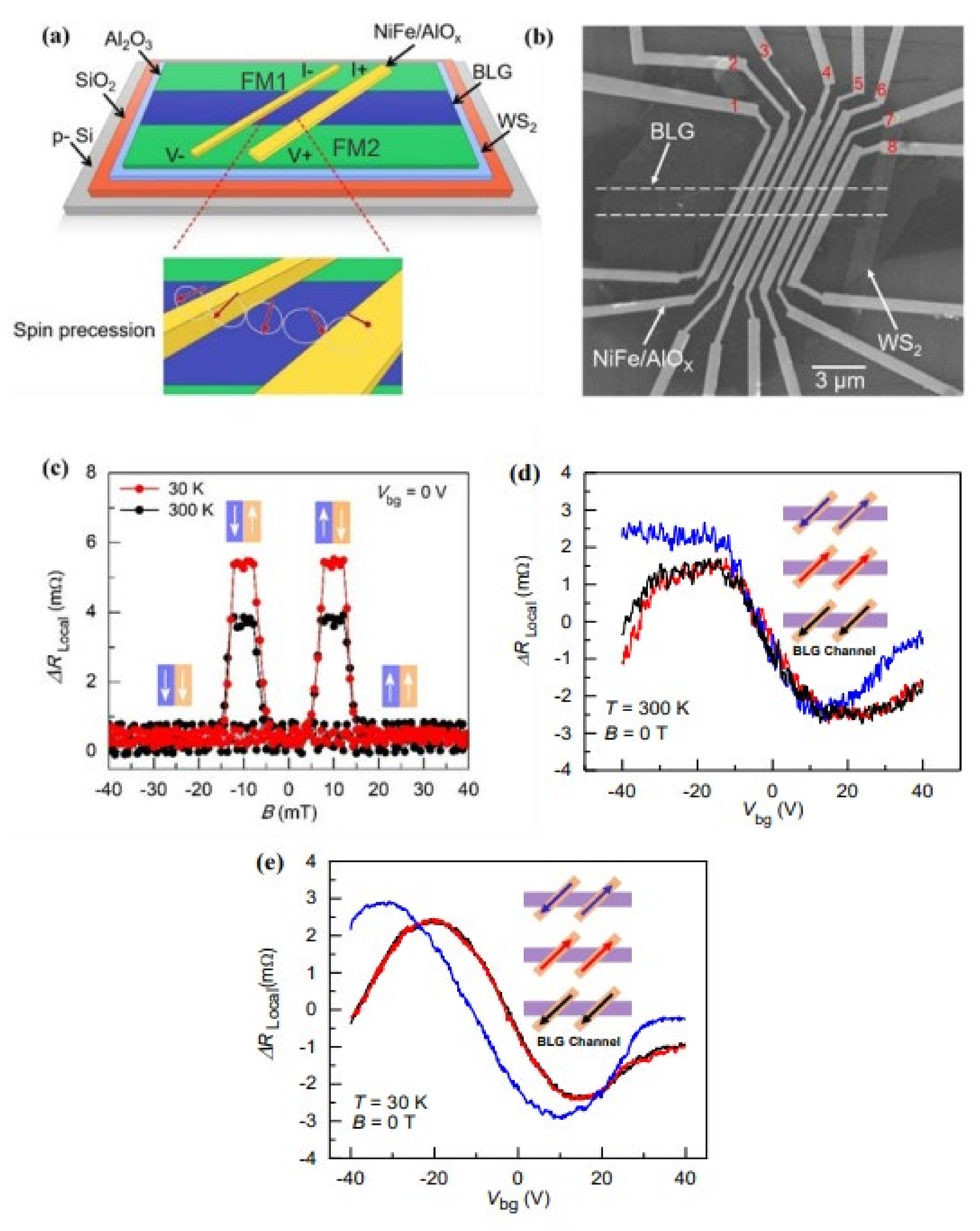
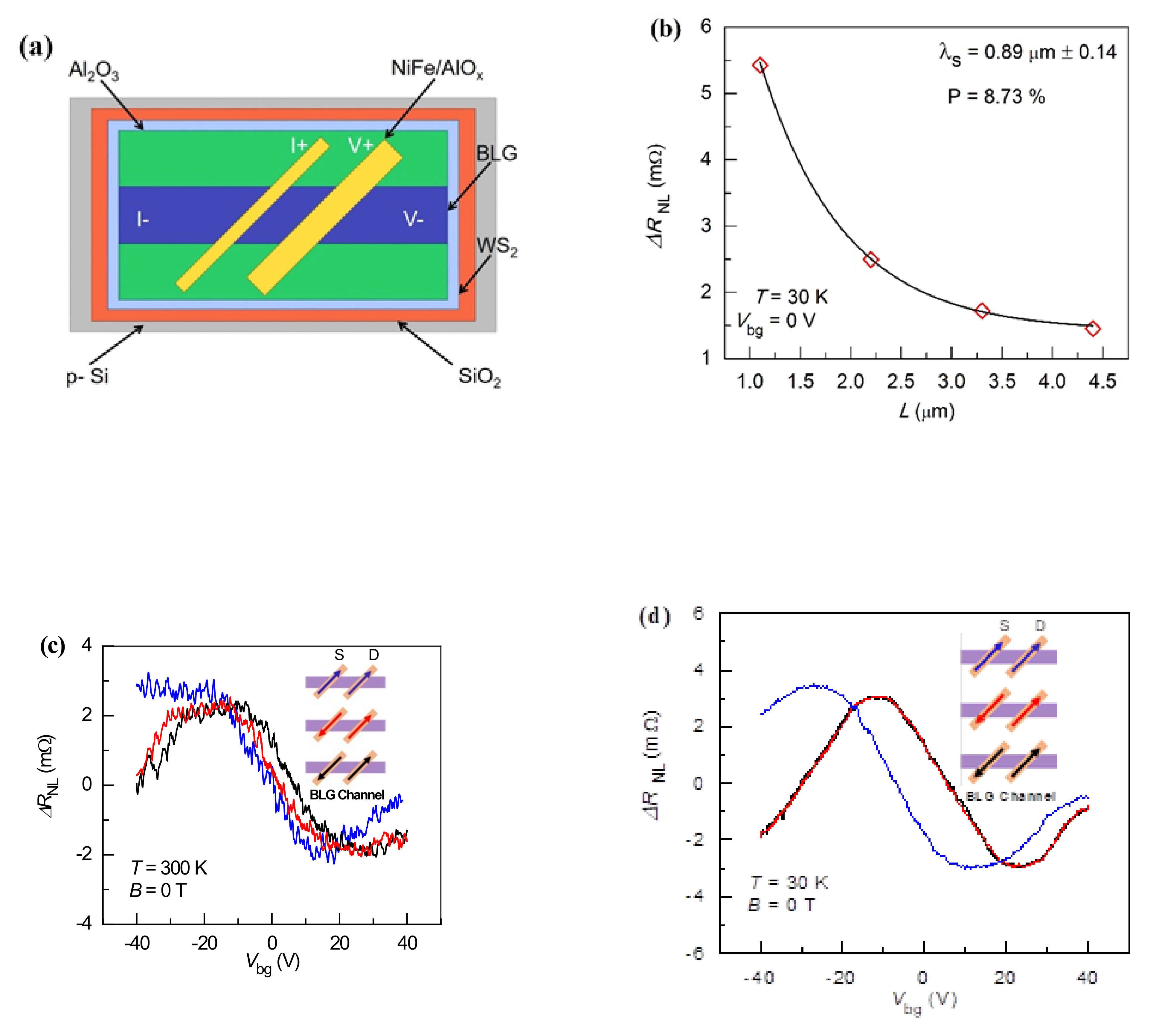
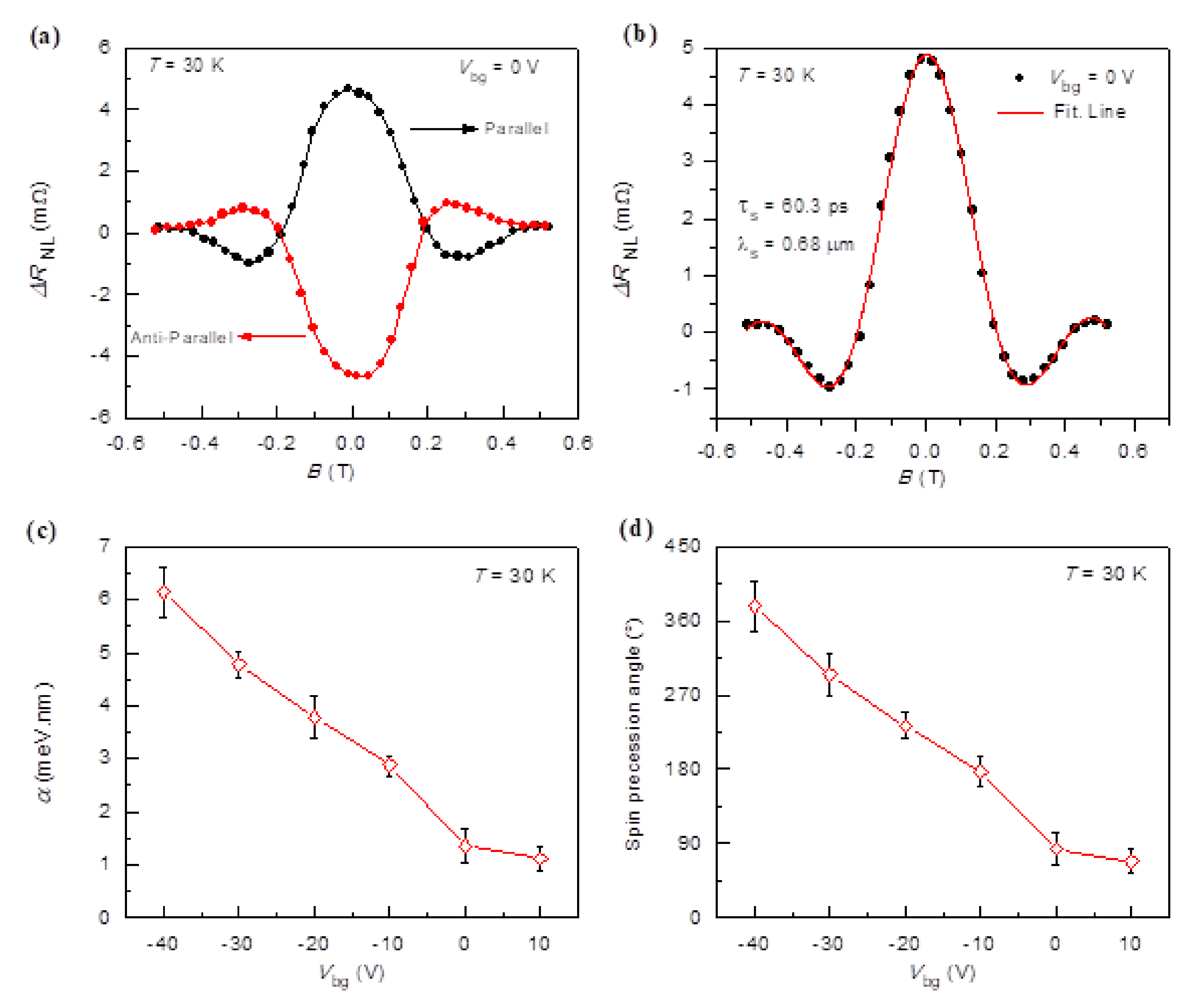
2. Experimental Section

ML-WS2 nanoflakes were mechanically exfoliated on p-type Si/SiO2 (300 nm) substrates acting as a back-gate with the help of standard mechanical exfoliation using Scotch tape. First, we placed the BLG on top of polydimethylsiloxane (PDMS) by mechanical exfoliation from commercial graphite and transferred it onto the WS2 flake. The thickness of BLG can be identified on the substrate because of the interference effect. Further, Raman spectroscopy and AFM were utilized to confirm the thickness. By using a micro-aligner stage, the flake of BLG was transferred onto the ML-WS2 flake. The device was placed in a furnace for annealing at 200 °C under gas flow at a rate of 97.5% Ar/2.5% H2 for 6 h.
To prevent direct contact of the FM electrode with WS2, the naked areas of WS2 were covered with 10 nm thick Al2O3 by atomic layer deposition (ALD). The FM electrodes were patterned by electron-beam lithography (E-beam lithography), and then aluminum (0.8 nm thick) was deposited by thermal evaporation and left to oxidize in an O2 atmosphere for 30 m before depositing 50 nm thick Ni81Fe19 by electron-beam evaporation. A thin layer of Al2O3 (t = 0.8 nm) was used as a tunnel barrier between the FM electrode and the BLG to resolve conductance mismatch problems in the spin injection [29,30,31]. After FM deposition, the samples were placed into acetone for lift-off.

3. Results and Discussion

Figure 1a shows a schematic of the BLG/ML-WS2 van der Waals (vdW) heterostructure spin FET; the bottom view illustrates the complete process of spin precession, and the top view represents the local measurement configuration. The widths of FM1 and FM2 were 0.3 μm and 1 μm, respectively. The width of the graphene channel was 2.3 μm. The 1 μm long BLG channel resistance was ~1.178 KΩ. A constant spin current was injected from FM1 electrode (source), and the spin signal was detected at FM2 electrode (drain). Basically, an in-plane magnetic field ( B ) was applied along the easy axes to align the magnetization in the same direction. The back gate voltage was applied to control the spin of electrons during the transport through the BLG channel. Figure 1b displays a scanning electron microscope image of the final device in which the FM electrode is patterned at 45° with respect to the BLG channel (the white dotted line) on WS2. The complete optical image of the spin FET in which the WS2 nanoflake is placed on SiO2 (300 nm thick) serves as the dielectric gate with a highly p-doped Si wafer prepared using the mechanical exfoliation method. Subsequently, BLG was transferred to WS2 by the dry transfer method illustrated in Figure S2a.
Atomic force microscopy (AFM) was used to confirm the thickness of ML-WS2 and BLG on SiO2 (Figure S2b). The height profiles reveal the thickness of ML-WS2 (~19 nm) and BLG (~0.8 nm) in Figure S2c,d, respectively. The Raman spectra of ML-WS2 and BLG on SiO2 are shown in Figure S3a,b, respectively. The Raman spectra of ML-WS2 and BLG on SiO2 are shown in Figure S3a,b. The E2g1 and A1 peaks of WS2 appear at 351 cm−1 and 418 cm−1, respectively. In the case of BLG, the Raman G and 2D peaks appear around 1587 cm−1 and 2685 cm−1, respectively. The ratio of intensities of the G to 2D peaks (I2D/IG) is ~1.2, which is consistent with the previously reported value for BLG [32]. Further, the 2D peak is fitted by four Lorentzian peaks, which confirms the nature of BLG (Figure S3c).
First, the basic electrical transport properties of Gr/WS2 vdW heterostructure devices (sample # 2) were characterized to confirm the disappearance of the Dirac point in the case of the FM electrode. In this regard, we measured the BLG on SiO2 and WS2 with different contacts such as Cr/Au and NiFe, as shown in Figure S4a. In fact, the Dirac point is shifted at a higher Vbg~30 V due to p-type doping of BLG by NiFe electrodes.
When the BLG/WS2 heterostructure device with FM electrode was measured, a very small change in resistance was found between Vbg = −40 V and +40 V because the bottom WS2 layer started to conduct (Figure S4b) and behaved like a sink of the back gate electrical field at Vbg > 10 V, as shown in Figure S4c. To examine the spin valve behavior in the BLG/ML-WS2 spin FET on SiO2, local spin valve (LSV) measurements were conducted at room temperature (300 K) and 30 K. The local configuration is shown in Figure 1a. The local spin value measurements of the BLG/ML-WS2 spin FET were performed by a standard lock-in technique using an AC excitation current of 9.88 μA. The spin signal was injected from one FM electrode (source) and detected from another FM electrode (drain) by applying the magnetic field (B) in the direction of the FM electrode. We applied a constant current between the two FM (7 and 8 in Figure 1b) electrodes and measured the voltage drop between these same two electrodes but opposite side contacts.
Initially, an in-plane magnetic field ( B ) was applied along the easy axes to align the magnetization in the same direction. The FM contacts have different coercivities because they are designed with different widths (0.3 and 1 μm). The magnetization configuration of FM contacts (injector and detector) can be aligned parallel or anti-parallel by sweeping an in-plane magnetic field, which results in magnetoresistance Δ R L o c a l = Δ V L o c a l I . A clear and noticeable local spin signal was detected at different temperatures, indicating spin transport in the BLG/ML-WS2 spin FET (Figure 1c).
We also measured the local signal as a function of Vbg at different temperatures and B = 0 T for each magnetization alignment of the injector (source) and detector (drain), as shown in the inset of Figure 1d,e. For all magnetization configurations, we observed clear oscillations of the local spin signal as a function of Vbg at room temperature (Figure 1d). This is the first demonstration of 300 K spin FET operation. Spin FET was also demonstrated at 30 K (Figure 1e). The half oscillation angle Δ θ   180 ° was observed for the change of back-gate voltage Δ V b g 40   V in both antiparallel and parallel states [33]. We found that the spin signal is less sensitive to Vbg when Vbg > 10 V. This is because ML-WS2 is an n-type TMD semiconductor material that begins to conduct and behaves like a sink at a positive Vbg, where electrons start to accumulate at the surface of WS2.
Therefore, the WS2 film screens the back-gate electric fields. However, the charge carriers in WS2 are much smaller than in BLG and thus contribute insignificantly to transport. In heterostructures like our BLG/ML-WS2 spin FET, a robust local electric field is engendered by the accumulation of electrons at the interface of BLG with WS2. The direction of this local electric field ( E z ) is perpendicular to the motion of electrons. It is expected that the coupling of this local field produces a Rashba-type SOI. This kind of SOI is defined by the Rashba Hamiltonian [28]
H R = α   σ   × k F   ·   z
where σ is the Pauli matrix, k F denotes the electron wave vector, and z is a unit vector perpendicular to the interface that defines the direction of spin precession and the effective magnetic field [34,35]. In this relation, the crucial parameter α represents the strength of the SOI, which is directly proportional to the interfacial electric field   E z   α     E z . The   E z   of the Rashba-type SOI strength   ( α ) originates from both the microscopic Coulomb potential and macroscopic potential gradient triggered by the hetero-interface and band bending in heterostructure devices of semiconductor materials. The macroscopic electric field can therefore be controlled by an external gate voltage applied to 2D systems and enhance the Rashba SOI [28,36]. This permits us to electrically modulate the effective magnetic field [37]. Thus, in our case, the interface of BLG with WS2 and the proximity effect of 2D materials enhances the strength of the Rashba-type SOI [15,28,38]. To probe the spin transport behavior and pure spin current in the BLG/ML-WS2 spin FET, an NL spin valve (NLSV) four-probe measurement scheme was used (Figure 2a). In order to examine the spin diffusion length ( λ s ) from spin valve measurements (Figure S6a), we measured the NL signal ( Δ R N L ) at different distances between the injector and detector (L). The NL spin value measurements of the BLG/ML-WS2 spin FET were performed by standard lock-in technique using an AC excitation current of 9.88 μA.
For the NL signal   R N L , a constant current was applied between the FM electrodes (7 and 8 in Figure 1b) and the NL voltage was measured at both FM contacts (6 and 5 in Figure 1b). Similar to the NL measurements, to measure the NL spin signals, we first applied a constant current and swept the B magnetic field along the easy axes to align the relative magnetization of the FM contacts. The difference in magnetization of the FM contacts gave rise to a sharp transition in NL magnetoresistance R N L = V N L I at both room temperature and 30 K. The NL signal decayed exponentially when increasing L, as shown in Figure 2b. We can evaluate λ s by using the relation [39]
Δ R N L = P 2 R t λ s e L λ s 2 w
where L is the spacing between the injector and detector, w is the width of the BLG channel, P is the spin polarization of the FM contacts, and R t   is the sheet resistance. By fitting the NL spin valve signal to Equation (2), we obtained λ s and contact polarization ( λ s   = 0.90   μ m ; P = 8.4%), as shown in Figure 2b. Further, we measured the NLSV signal as a function of Vbg at room temperature and 30 K (Figure 2c,d). The inset shows the alignment of magnetization for antiparallel and parallel states. Similar to the local measurement, we first used the magnetization configuration and then measured the change in R N L as a function of Vbg at B = 0 T. We observed complete oscillation of the NLSV signal as a function of Vbg for each magnetization configuration of the FM electrodes. The characteristics of the oscillation in the NLSV signal are almost the same as for the local spin valve signals. The Hanle NLSV signal was measured using the configuration shown in Figure 2a.
As expected, we obtained an NL Hanle spin precession signal of Δ R N L 6.9   m Ω with a separation of L  1   μ m (center-to-center distance) between the FM electrodes, as shown in Figure 3a. In this type of geometry, the Hanle spin signal stems from the spin precession about B with the Larmor frequency given by ω L = g μ B   B , where g is the Landé factor, μ B is the Bohr magneton, and is the Planck constant divided by 2π. The variation in Δ R N L due to spin precession and spin diffusion relaxation from the source to drain can be defined by
Δ R N L   0 1 4 π D s t e L 2 4 D s t cos   ( ω L t )   e t τ s d t
By fitting the raw data of the Hanle spin signal, we extracted the spin lifetime ( τ s ) in the range of τ s 66.05 2.02   ps depending on Vbg. This is in the same range of previously reported values [40,41,42]. We assume that the spin diffusion constant (Ds) is the same as the charge diffusion constant (D).
Further, we calculated the spin diffusion length ( λ s = D s τ s ) as being in the range of 0.98 0.15   μ m depending on Vbg. The gate dependent τs and λs are shown in Figure S6a,b, respectively. Figure 3a shows the fitting of the Hanle data when Vbg = 0 V. The spin diffusion length estimated from the Hanle measurement (λs = 0.68 μm) is nearly the same as that estimated by the NL spin valve signal fitting (λs = 0.89 μm, Figure 2b). Our BLG/ML-WS2 spin FET τ s is very small compared to pristine graphene, which ranges from 168 to 447 ps, [43] which is indicative of the existence of a proximity-induced SOI in BLG through the WS2 film. Such a small τ s has also been predicted by using the spin-orbit relaxation time ( τ s o ) calculated from the spin Hall effect (SHE), WAL, and from theoretical predictions [20].
Next, we appraised the prevailing spin scattering mechanisms in our BLG/ML-WS2 spin FET by estimating spin relaxation time ( τ s ) and momentum scattering time ( τ P ). First, we calculated τ P from   D = ν F 2 τ P , where vF is the Fermi velocity. For the BLG on WS2, we obtained D by using the Einstein relation σ = e 2 D   N 2 D E F , where N 2 D E F is the density of states of graphene at the Fermi level [44]. In BLG, the D’yakonov-Perel’ (DP) mechanism is dominant because τ s is inversely proportional to τ P [10,43]. Therefore, we further investigated the Rashba-type SOI using   1 τ s = 4 Δ R 2 2   τ P . The calculated value of ΔR (~17.15 meV) in our BLG/ML-WS2 spin FET was much larger than the theoretically and experimentally predicted value of graphene on a conventional 2D substrates [21,42,45], which is analogous to our previous work [28].
It is worthwhile noting that ΔR can be modified by Vbg more effectively in BLG than in SLG; when Vbg < 0, ΔR is more sensitive to Vbg, but when Vbg > 0, we found that the change in ΔR is small due to the screening effect of gate electric fields by the n-type WS2 film (Figure S6c). Furthermore, we calculated the Rashba-type SOI strength (α) by using the following relation [28]:
τ s = 4 4 α   2 D   m *   2
where m* is the effective mass of electrons and holes in BLG [46]. The estimated value of α is 6.14 meVnm, which is much higher compared to that of pristine graphene. Figure 3c shows α of the BLG/ML-WS2 device as a function of Vbg. For Vbg < 0, Vbg efficiently changes   α , whereas α does not change much when Vbg > 0 due to the screening effect of the n-type WS2 film. Finally, from the Rashba parameter, we obtained the spin precession angle with respect to Vbg (Figure 3d) by the following relation [5]:
Δ θ =   2 m * α L 2
where m* is the effective mass of electrons and holes in BLG, L 1   μ m is separation (center-to-center distance) between the FM electrodes, and ħ is the Planck constant divided by 2π. The amount of spin precession is determined by α, which depends on Vbg. We have described the schematic spin precession in Figure 1a. In the BLG/ML-WS2 spin FET, the injected spins are initially aligned in the direction of magnetization of the FM source.
In the channel, a moving electron k x under an electric field E z experiences an effective magnetic field B R y called the Rashba field. The precessional rate changes with Vbg because the Rashba field is proportional to Ez. When Vbg changes from −40 to +10 V in our BLG/ML-WS2 spin FET, the total change of precession angle is Δ θ     309 ° (Figure 3d). The change in precession angle is Δ θ = 180 ° when Vbg changes from −30 to 0 V, which explains the observed gate dependent local and NL spin signals at B = 0 T. These findings provide the first step for successfully realizing a graphene-based spin FET.

4. Conclusions

In summary, we successfully fabricated a novel BLG/ML-WS2 spin FET to realize gate controlled spin precession. One promising outcome was the enhanced Rashba SOI in the BLG/ML-WS2 heterostructure, as this offers the creation of a pure spin current by the SHE or the manipulation of spin through an electric field. The key parameters of spin transport (e.g.,   τ s ,   λ s , and α ) have been derived as a function of Vbg. Moreover, we showed that the change of α as a function of Vbg explains gate controlled spin precession in the BLG/ML-WS2 spin FET. The gate control of spin precession at room temperature is an interesting step in the field of spintronics. These outcomes may open a new platform for the manipulation of spin current, precession, and spin degree of freedom of electrons.

Supplementary Materials

The following are available online at https://www.mdpi.com/article/10.3390/electronics10222879/s1, Figure S1: Schematic diagram showing fabrication process flow of graphene/WS2 field-effect transistors heterostructure device. (a)–(e) Schematic procedures of the device fabrication. Figure S2: Structure of the BLG/ML-WS2 spin FET. (a) An optical microscope image of the BLG/ML-WS2 heterostructure device with FM source and drain contact with local measurement geometry. The FM electrodes are patterned at 45° with respect to the BLG channel. The length and width of the graphene channel were 1 μm and 2.3 μm, respectively. (b) AFM image of the device showing WS2 and BLG on SiO2. (c) The height profile of WS2. The thickness of the WS2 is ~19 nm. (d) The height profile of BLG. The thickness of the BLG flake is ~0.8 nm. Figure S3: Raman spectra of the BLG/ML-WS2 spin FET. (a) Raman spectrum of multilayers of WS2. The peaks E12g and A1 appear at 351 cm−1 and 418 cm−1, respectively. (b) Raman spectrum of BLG. (c) Raman spectrum of BLG 2D peak. The peak is fitted by four Lorentzian peaks, which confirms the nature of BLG. Figure S4: Doping effect by NiFe electrodes and screening effect by WS2 layer. (a) An optical image of the final device in which graphene is marked with the white dashed line on SiO2 and WS2 (sample #2). The different pairs of NiFe and Cr/Au electrodes were patterned by electron-beam lithography on WS2, BLG, and BLG/WS2 heterostructure devices, which is illustrated by purple, red, green, orange, and blue circles for WS2 (Cr/Au), BLG (Cr/Au), BLG/WS2 (Cr/Au), BLG/WS2 (NiFe), and BLG (NiFe), respectively. (b) The transfer characteristics as a function of Vbg of WS2 with Cr/Au (purple circle); the threshold voltage (Vth) was found around 10 V. (c) The resistance of BLG on SiO2 and WS2 as a function of back gate voltage (Vbg) with different electrodes. Figure S5: Gate modulation of spin precession angle in the BLG/ML-WS2 spin FET. (a) Modulation of Hanle spin precession with back-gate voltage. Hanle spin signal measured at different back gates at 30 K. (b) Gate voltage dependence of the spin-orbit interaction parameter α. (c) Estimated spin precession angle as a function of Vbg at 30 K. Figure S6: Spin transport parameters. (a) Gate dependence of τs, which is derived from the fitting of the Hanle spin precession in Equation (3). (b) Gate dependence of λs. (c) Rashba spin-splitting (∆R) as a function of Vbg at 30 K. Table S1: Comparison of key parameters of bilayer graphene/multilayer WS2 field-effect transistor with previously reported parameters in pristine graphene.

Author Contributions

A.M.A. and J.E. conceived the work, designed the research strategy, analyzed data, and wrote the paper. A.M.A. and M.F.K. performed the experiments. J.E. directed the project. All authors have read and agreed to the published version of the manuscript.

Funding

This work was supported by the grant No. 2021R1A4A1031900, the Basic Science Research Program (2019R1F1A1057697), and the Global Research and Development Center Program (2018K1A4A3A01064272) through the National Research Foundation of Korea (NRF) grant funded by the Korea government (Ministry of Education and the Ministry of Science and ICT).

Conflicts of Interest

The authors declare no conflict of interest.

References

  1. Fert, A. Nobel Lecture: Origin, development, and future of spintronics. Rev. Mod. Phys. 2008, 80, 1517–1530. [Google Scholar] [CrossRef] [Green Version]
  2. Awschalom, D.D.; Flatté, M.E. Challenges for semiconductor spintronics. Nat. Phys. 2007, 3, 153. [Google Scholar] [CrossRef]
  3. Datta, S.; Das, B. Electronic analog of the electro-optic modulator. Appl. Phys. Lett. 1990, 56, 665–667. [Google Scholar] [CrossRef]
  4. Chuang, P.; Ho, S.-C.; Smith, L.W.; Sfigakis, F.; Pepper, M.; Chen, C.-H.; Fan, J.-C.; Griffiths, J.P.; Farrer, I.; Beere, H.E.; et al. All-electric all-semiconductor spin field-effect transistors. Nat. Nanotechnol. 2014, 10, 35. Available online: https://www.nature.com/articles/nnano.2014.296#supplementary-information (accessed on 22 December 2014). [CrossRef] [PubMed] [Green Version]
  5. Koo, H.C.; Kwon, J.H.; Eom, J.; Chang, J.; Han, S.H.; Johnson, M. Control of Spin Precession in a Spin-Injected Field Effect Transistor. Science 2009, 325, 1515–1518. [Google Scholar] [CrossRef] [PubMed]
  6. Wunderlich, J.; Park, B.-G.; Irvine, A.C.; Zârbo, L.P.; Rozkotová, E.; Nemec, P.; Novák, V.; Sinova, J.; Jungwirth, T. Spin Hall Effect Transistor. Science 2010, 330, 1801–1804. [Google Scholar] [CrossRef] [PubMed] [Green Version]
  7. Semenov, Y.G.; Kim, K.W.; Zavada, J.M. Spin field effect transistor with a graphene channel. Appl. Phys. Lett. 2007, 91, 153105. [Google Scholar] [CrossRef]
  8. Novoselov, K.S.; Geim, A.K.; Morozov, S.V.; Jiang, D.; Zhang, Y.; Dubonos, S.V.; Grigorieva, I.V.; Firsov, A.A. Electric Field Effect in Atomically Thin Carbon Films. Science 2004, 306, 666–669. [Google Scholar] [CrossRef] [Green Version]
  9. Wen, H.; Dery, H.; Amamou, W.; Zhu, T.; Lin, Z.; Shi, J.; Žutić, I.; Krivorotov, I.; Sham, L.J.; Kawakami, R.K. Experimental Demonstration of xor Operation in Graphene Magnetologic Gates at Room Temperature. Phys. Rev. Appl. 2016, 5, 044003. [Google Scholar] [CrossRef] [Green Version]
  10. Han, W.; Kawakami, R.K.; Gmitra, M.; Fabian, J. Graphene spintronics. Nat. Nanotechnol. 2014, 9, 794. [Google Scholar] [CrossRef]
  11. Geim, A.K.; Novoselov, K.S. The rise of graphene. Nat. Mater. 2007, 6, 183. [Google Scholar] [CrossRef]
  12. Panda, J.; Ramu, M.; Karis, O.; Sarkar, T.; Kamalakar, M.V. Ultimate Spin Currents in Commercial Chemical Vapor Deposited Graphene. ACS Nano 2020, 14, 12771–12780. [Google Scholar] [CrossRef]
  13. Calleja, F.; Ochoa, H.; Garnica, M.; Barja, S.; Navarro, J.J.; Black, A.; Otrokov, M.M.; Chulkov, E.V.; Arnau, A.; Vázquez de Parga, A.L.; et al. Spatial variation of a giant spin–orbit effect induces electron confinement in graphene on Pb islands. Nat. Phys. 2014, 11, 43. Available online: https://www.nature.com/articles/nphys3173#supplementary-information (accessed on 15 December 2014). [CrossRef]
  14. Balakrishnan, J.; Kok Wai Koon, G.; Jaiswal, M.; Castro Neto, A.H.; Özyilmaz, B. Colossal enhancement of spin–orbit coupling in weakly hydrogenated graphene. Nat. Phys. 2013, 9, 284. Available online: https://www.nature.com/articles/nphys2576#supplementary-information (accessed on 17 March 2013). [CrossRef] [Green Version]
  15. Avsar, A.; Tan, J.Y.; Taychatanapat, T.; Balakrishnan, J.; Koon, G.K.W.; Yeo, Y.; Lahiri, J.; Carvalho, A.; Rodin, A.S.; O’Farrell, E.C.T.; et al. Spin–orbit proximity effect in graphene. Nat. Commun. 2014, 5, 4875. Available online: https://www.nature.com/articles/ncomms5875#supplementary-information (accessed on 31 July 2014). [CrossRef]
  16. Wang, Q.H.; Kalantar-Zadeh, K.; Kis, A.; Coleman, J.N.; Strano, M.S. Electronics and optoelectronics of two-dimensional transition metal dichalcogenides. Nat. Nanotechnol. 2012, 7, 699. [Google Scholar] [CrossRef]
  17. Zhu, Z.Y.; Cheng, Y.C.; Schwingenschlögl, U. Giant spin-orbit-induced spin splitting in two-dimensional transition-metal dichalcogenide semiconductors. Phys. Rev. B 2011, 84, 153402. [Google Scholar] [CrossRef] [Green Version]
  18. Xiao, D.; Liu, G.-B.; Feng, W.; Xu, X.; Yao, W. Coupled spin and valley physics in monolayers of MoS2 and other group-VI dichalcogenides. Phys. Rev. Lett. 2012, 108, 196802. [Google Scholar] [CrossRef] [Green Version]
  19. Nitta, J.; Akazaki, T.; Takayanagi, H.; Enoki, T. Gate Control of Spin-Orbit Interaction in an Inverted In0.53Ga0.47 As/In0.52Al0.48As Heterostructure. Phys. Rev. Lett. 1997, 78, 1335. [Google Scholar] [CrossRef]
  20. Wang, Z.; Ki, D.K.; Chen, H.; Berger, H.; MacDonald, A.H.; Morpurgo, A.F. Strong interface-induced spin–orbit interaction in graphene on WS2. Nat. Commun. 2015, 6, 8339. Available online: https://www.nature.com/articles/ncomms9339#supplementary-information (accessed on 21 August 2015). [CrossRef] [Green Version]
  21. Wang, Z.; Ki, D.-K.; Khoo, J.Y.; Mauro, D.; Berger, H.; Levitov, L.S.; Morpurgo, A.F. Origin and Magnitude of ‘Designer’ Spin-Orbit Interaction in Graphene on Semiconducting Transition Metal Dichalcogenides. Phys. Rev. X 2016, 6, 041020. [Google Scholar] [CrossRef]
  22. Island, J.O.; Cui, X.; Lewandowski, C.; Khoo, J.Y.; Spanton, E.M.; Zhou, H.; Rhodes, D.; Hone, J.C.; Taniguchi, T.; Watanabe, K.; et al. Spin–orbit-driven band inversion in bilayer graphene by the van der Waals proximity effect. Nature 2019, 571, 85–89. [Google Scholar] [CrossRef] [PubMed] [Green Version]
  23. Safeer, C.K.; Ingla-Aynés, J.; Herling, F.; Garcia, J.H.; Vila, M.; Ontoso, N.; Calvo, M.R.; Roche, S.; Hueso, L.E.; Casanova, F. Room-Temperature Spin Hall Effect in Graphene/MoS2 van der Waals Heterostructures. Nano Lett. 2019, 19, 1074–1082. [Google Scholar] [CrossRef] [PubMed] [Green Version]
  24. Wakamura, T.; Wu, N.J.; Chepelianskii, A.D.; Guéron, S.; Och, M.; Ferrier, M.; Taniguchi, T.; Watanabe, K.; Mattevi, C.; Bouchiat, H. Spin-Orbit-Enhanced Robustness of Supercurrent in Graphene/WS2 Josephson Junctions. Phys. Rev. Lett. 2020, 125, 266801. [Google Scholar] [CrossRef]
  25. Ingla-Aynés, J.; Herling, F.; Fabian, J.; Hueso, L.E.; Casanova, F. Electrical Control of Valley-Zeeman Spin-Orbit-Coupling--Induced Spin Precession at Room Temperature. Phys. Rev. Lett. 2021, 127, 047202. [Google Scholar] [CrossRef]
  26. Omar, S.; Madhushankar, B.N.; van Wees, B.J. Large spin-relaxation anisotropy in bilayer-graphene/WS2 heterostructures. Phys. Rev. B 2019, 100, 155415. [Google Scholar] [CrossRef] [Green Version]
  27. Tiwari, P.; Srivastav, S.K.; Bid, A. Electric-Field-Tunable Valley Zeeman Effect in Bilayer Graphene Heterostructures: Realization of the Spin-Orbit Valve Effect. Phys. Rev. Lett. 2021, 126, 096801. [Google Scholar] [CrossRef]
  28. Afzal, A.M.; Khan, M.F.; Nazir, G.; Dastgeer, G.; Aftab, S.; Akhtar, I.; Seo, Y.; Eom, J. Gate Modulation of the Spin-orbit Interaction in Bilayer Graphene Encapsulated by WS2 films. Sci. Rep. 2018, 8, 3412. [Google Scholar] [CrossRef]
  29. Rashba, E.I. Theory of electrical spin injection: Tunnel contacts as a solution of the conductivity mismatch problem. Phys. Rev. B 2000, 62, R16267–R16270. [Google Scholar] [CrossRef] [Green Version]
  30. Schmidt, G.; Ferrand, D.; Molenkamp, L.W.; Filip, A.T.; van Wees, B.J. Fundamental obstacle for electrical spin injection from a ferromagnetic metal into a diffusive semiconductor. Phys. Rev. B 2000, 62, R4790–R4793. [Google Scholar] [CrossRef] [Green Version]
  31. Tombros, N.; Jozsa, C.; Popinciuc, M.; Jonkman, H.T.; van Wees, B.J. Electronic spin transport and spin precession in single graphene layers at room temperature. Nature 2007, 448, 571–574. [Google Scholar] [CrossRef] [Green Version]
  32. Ferrari, A.C.; Meyer, J.; Scardaci, V.; Casiraghi, C.; Lazzeri, M.; Mauri, F.; Piscanec, S.; Jiang, D.; Novoselov, K.; Roth, S. Raman spectrum of graphene and graphene layers. Phys. Rev. Lett. 2006, 97, 187401. [Google Scholar] [CrossRef] [Green Version]
  33. Park, Y.H.; Choi, J.W.; Kim, H.-J.; Chang, J.; Han, S.H.; Choi, H.-J.; Koo, H.C. Complementary spin transistor using a quantum well channel. Sci. Rep. 2017, 7, 46671. [Google Scholar] [CrossRef]
  34. Bychkov, Y.A.; Rashba, E.I. Oscillatory effects and the magnetic susceptibility of carriers in inversion layers. J. Phys. C Solid State Phys. 1984, 17, 6039. [Google Scholar] [CrossRef]
  35. Hikami, S.; Larkin, A.I.; Nagaoka, Y. Spin-Orbit Interaction and Magnetoresistance in the Two Dimensional Random System. Prog. Theor. Phys. 1980, 63, 707–710. [Google Scholar] [CrossRef]
  36. Yang, B.; Tu, M.-F.; Kim, J.; Wu, Y.; Wang, H.; Alicea, J.; Wu, R.; Bockrath, M.; Shi, J. Tunable spin–orbit coupling and symmetry-protected edge states in graphene/WS2. 2D Mater. 2016, 3, 031012. [Google Scholar] [CrossRef] [Green Version]
  37. Roland, W. Spin-orbit coupling effects in two-dimensional electron and hole systems. In Springer Tracts in Modern Physiscs; Springer: Berlin/Heidelberg, Germany, 2003; p. 191. [Google Scholar]
  38. Omar, S.; van Wees, B.J. Graphene-WS 2 heterostructures for tunable spin injection and spin transport. Phys. Rev. B 2017, 95, 081404. [Google Scholar] [CrossRef] [Green Version]
  39. Matsuki, K.; Ohshima, R.; Leiva, L.; Ando, Y.; Shinjo, T.; Tsuchiya, T.; Shiraishi, M. Spin transport in a lateral spin valve with a suspended Cu channel. Sci. Rep. 2020, 10, 10699. [Google Scholar] [CrossRef]
  40. Dankert, A.; Dash, S.P. Electrical gate control of spin current in van der Waals heterostructures at room temperature. Nat. Commun. 2017, 8, 16093. Available online: https://www.nature.com/articles/ncomms16093#supplementary-information (accessed on 25 May 2017). [CrossRef]
  41. Omar, S.; van Wees, B.J. Spin transport in high-mobility graphene on WS2 substrate with electric-field tunable proximity spin-orbit interaction. Phys. Rev. B 2018, 97, 045414. [Google Scholar] [CrossRef] [Green Version]
  42. Cummings, A.W.; Garcia, J.H.; Fabian, J.; Roche, S. Giant Spin Lifetime Anisotropy in Graphene Induced by Proximity Effects. Phys. Rev. Lett. 2017, 119, 206601. [Google Scholar] [CrossRef] [Green Version]
  43. Han, W.; Kawakami, R.K. Spin Relaxation in Single-Layer and Bilayer Graphene. Phys. Rev. Lett. 2011, 107, 047207. [Google Scholar] [CrossRef]
  44. Guimarães, M.H.D.; Zomer, P.J.; Ingla-Aynés, J.; Brant, J.C.; Tombros, N.; van Wees, B.J. Controlling Spin Relaxation in Hexagonal BN-Encapsulated Graphene with a Transverse Electric Field. Phys. Rev. Lett. 2014, 113, 086602. [Google Scholar] [CrossRef]
  45. Min, H.; Hill, J.E.; Sinitsyn, N.A.; Sahu, B.R.; Kleinman, L.; MacDonald, A.H. Intrinsic and Rashba spin-orbit interactions in graphene sheets. Phys. Rev. B 2006, 74, 165310. [Google Scholar] [CrossRef] [Green Version]
  46. Zou, K.; Hong, X.; Zhu, J. Effective mass of electrons and holes in bilayer graphene: Electron-hole asymmetry and electron-electron interaction. Phys. Rev. B 2011, 84, 085408. [Google Scholar] [CrossRef] [Green Version]
Figure 1. (a) Schematic representation of the BLG/ML-WS2 spin FET. (b) Scanning electron microscope image of a complete BLG spin FET. (c) LSV signal as a function of parallel magnetic field at 300 K and 30 K at Vbg = 0 V, where Δ R L o c a l = R   R p and R p = 1178.3   Ω . (d) LSV signal as a function of Vbg at B = 0 T and at T = 300 K for anti-parallel (blue line), parallel (red line), and parallel (black line), respectively. (e) LSV signal as a function of Vbg at B = 0 T and at 30 K for anti-parallel (blue line), parallel (red line), and parallel (black line), respectively. The LSV signals are moving-averaged to remove noise from a data set.
Electronics 10 02879 g001
Figure 2. (a) NL measurement configuration of spin injection and detection. (b) Exponential decay of the NLSV signal with L of injector and detector. (c) NLSV spin signal as a function of Vbg at B = 0 T and T = 300 K for parallel (blue line), anti-parallel (red line), and anti-parallel (black line), respectively. (d) NLSV spin signal as a function of Vbg at B = 0 T and at 30 K for parallel (blue line), anti-parallel (red line), and anti-parallel (black line), respectively. The NLSV signals are moving-averaged to remove noise from a data set.
Electronics 10 02879 g002
Figure 3. (a) Modulation of Hanle spin precession with Vbg. Hanle spin signal measured at different Vbg at 30 K. (b) The NL Hanle spin signal ( Δ R N L =   R N L P a r a l l e l R N L A n t i p a r a l l e l / 2 ) at Vbg = 0 V is fitted to Equation (3) for τ s and λ s . (c) Gate voltage dependence of the SOI parameter (α). (d) Estimated spin precession angle as a function of Vbg at 30 K.
Electronics 10 02879 g003
Publisher’s Note: MDPI stays neutral with regard to jurisdictional claims in published maps and institutional affiliations.

