
An Optimum Structure of Scalable Capacitors in 3D Crosspoint Memory Technology

Abstract
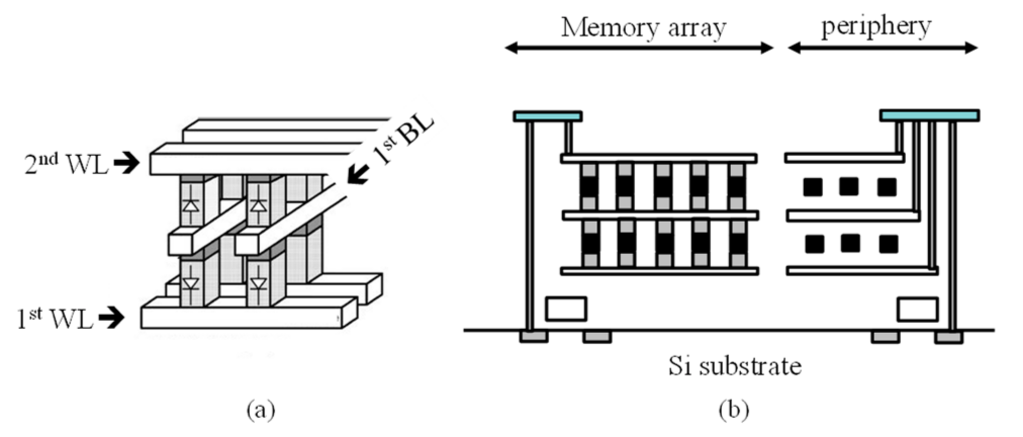
:1. Introduction
2. Capacitor Model
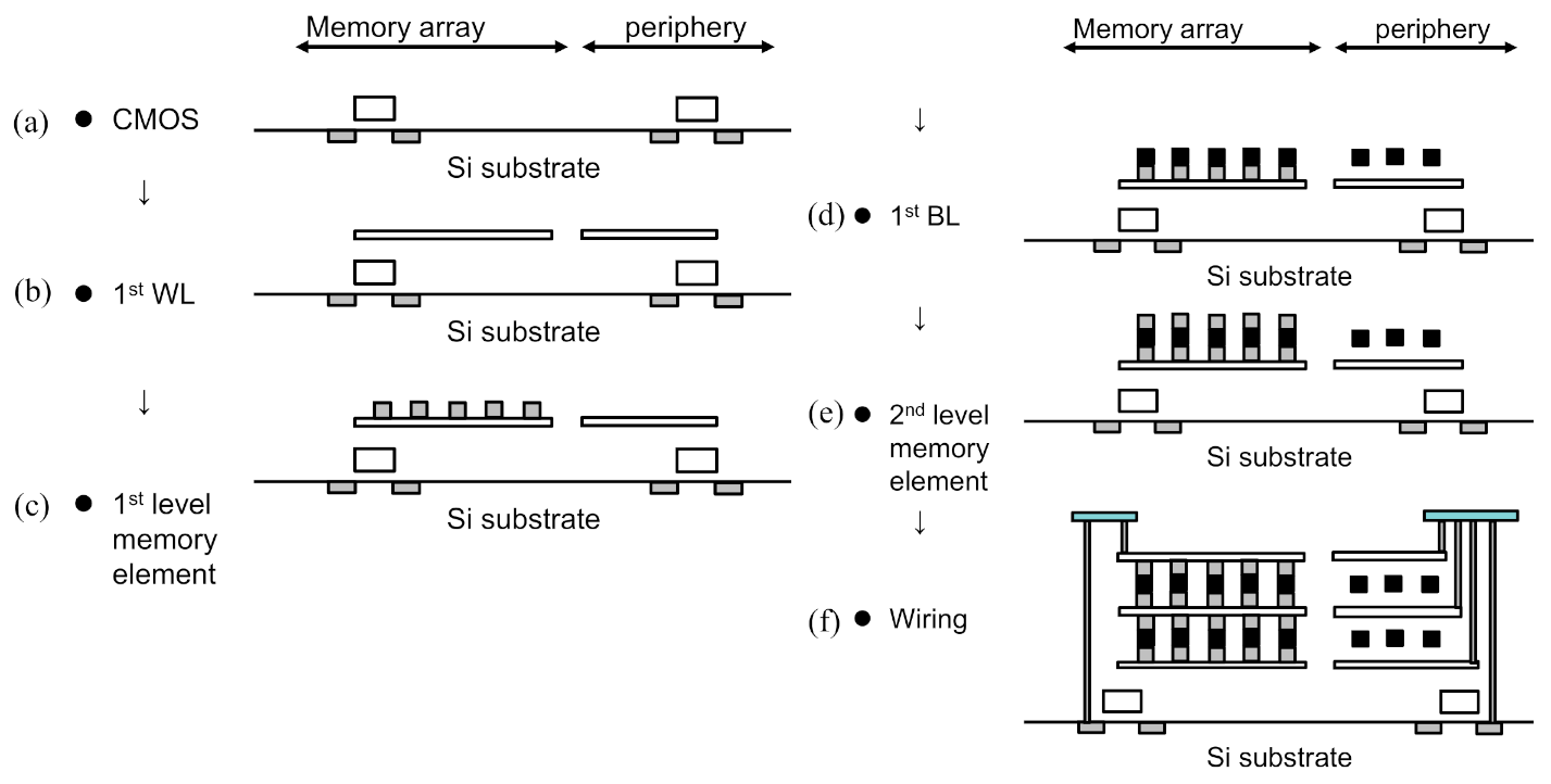
2.1. Fabrication Steps
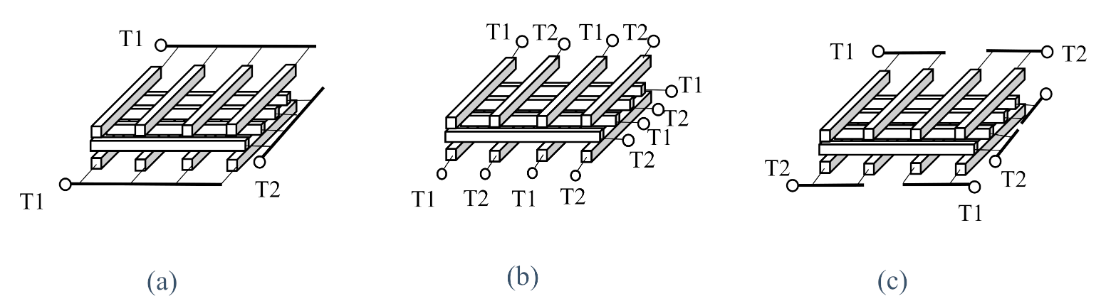
2.2. Three-Capacitor Structures Studied in This Paper
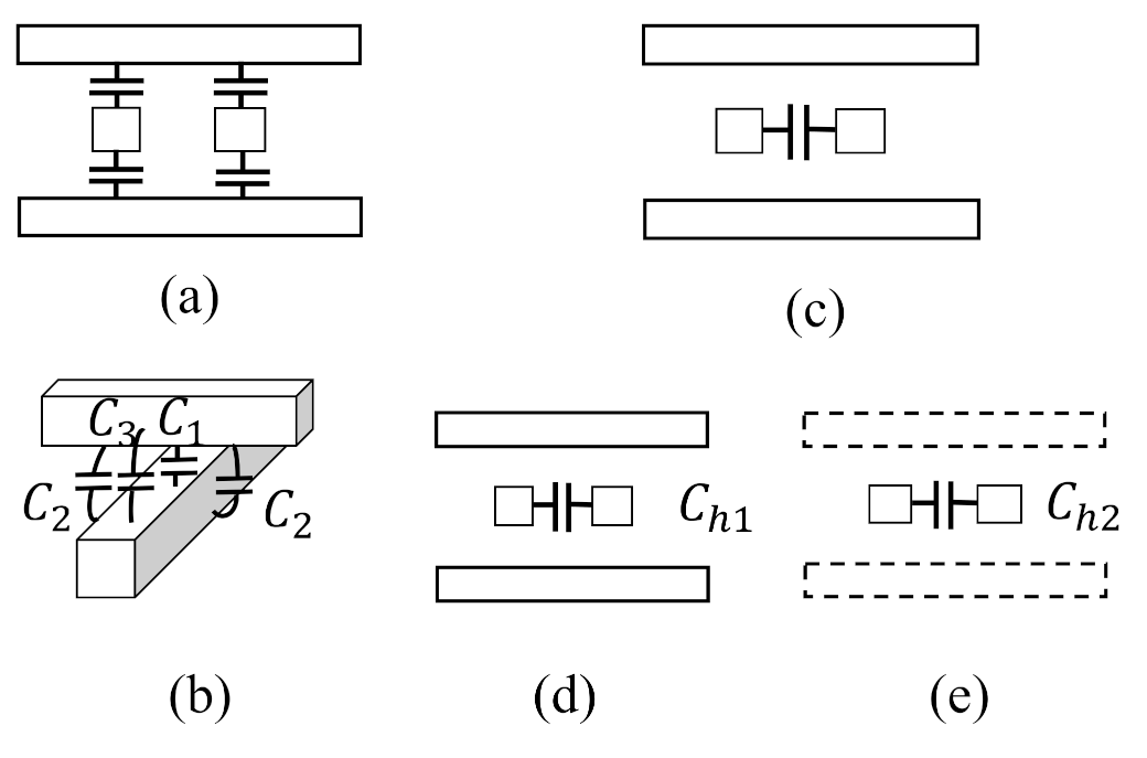
2.3. Modeling
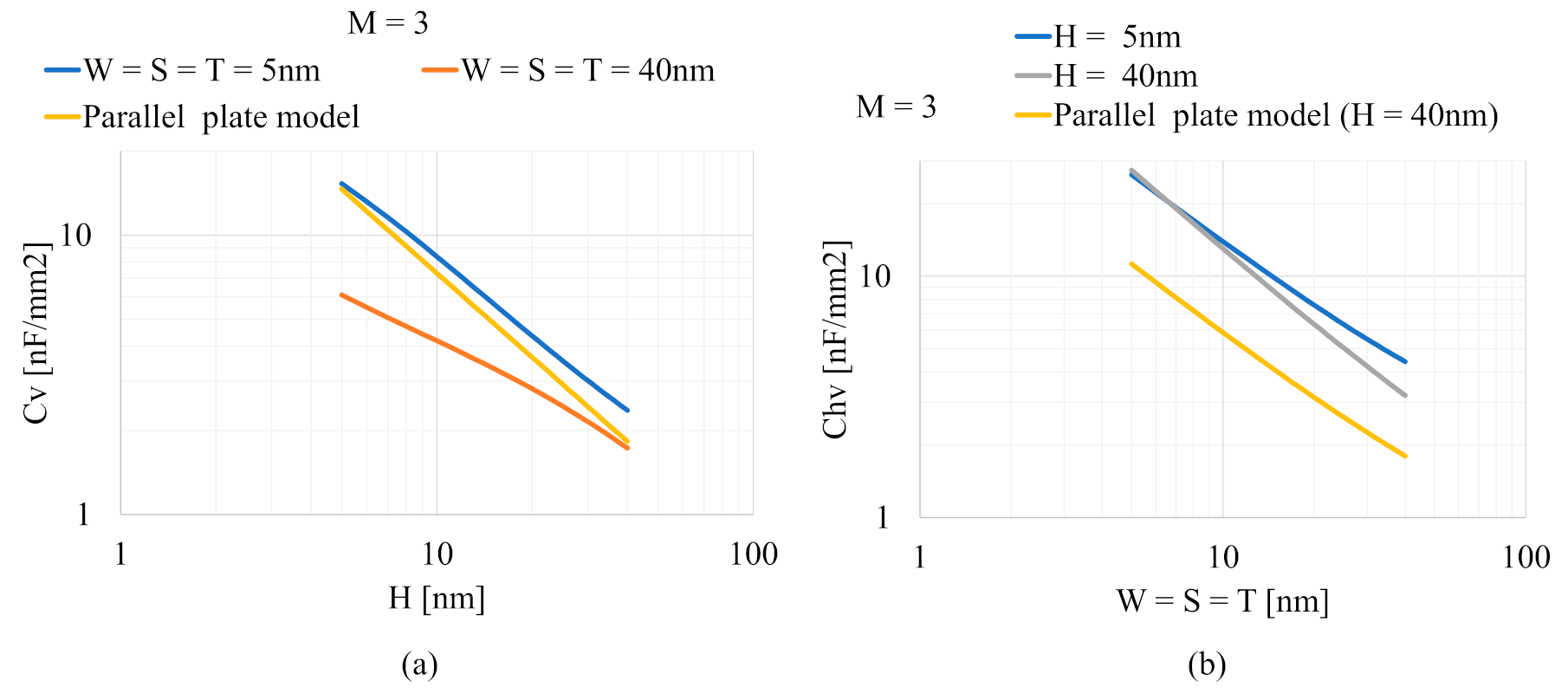
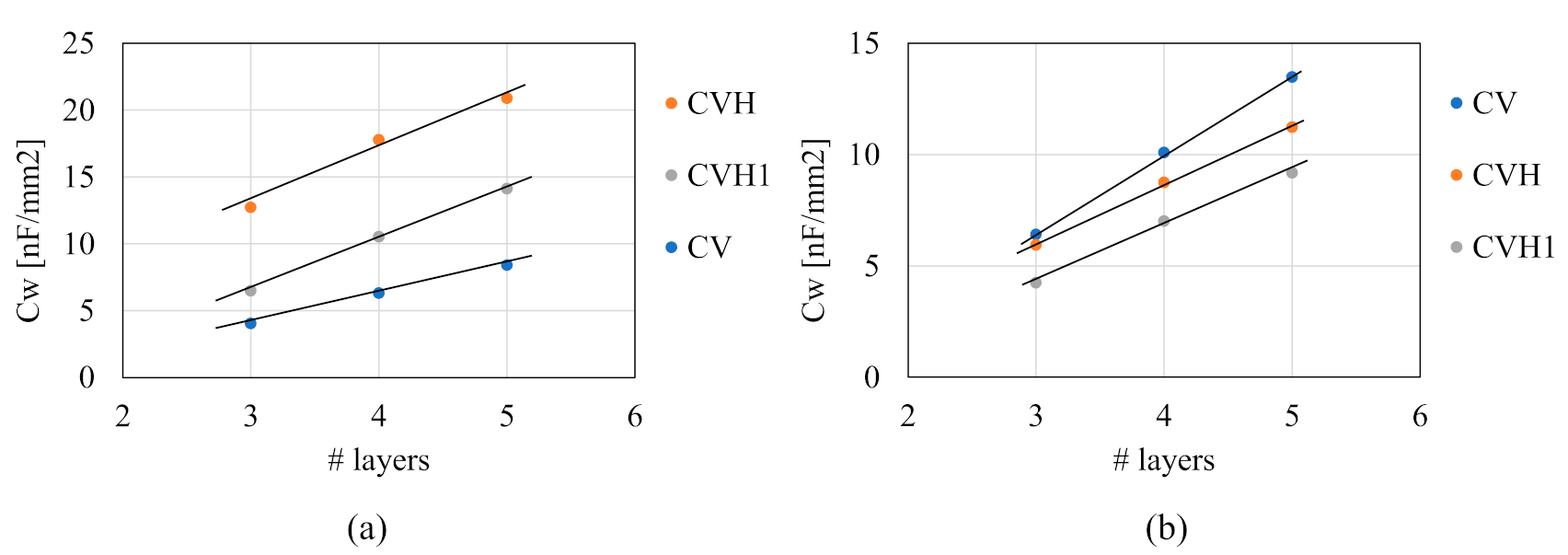
2.4. Comparison of the Capacitance Density between the Three Structures
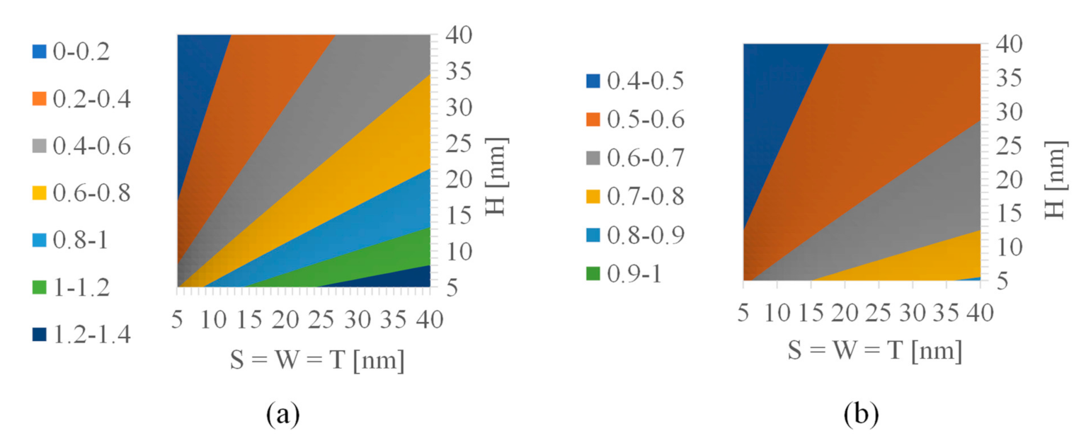
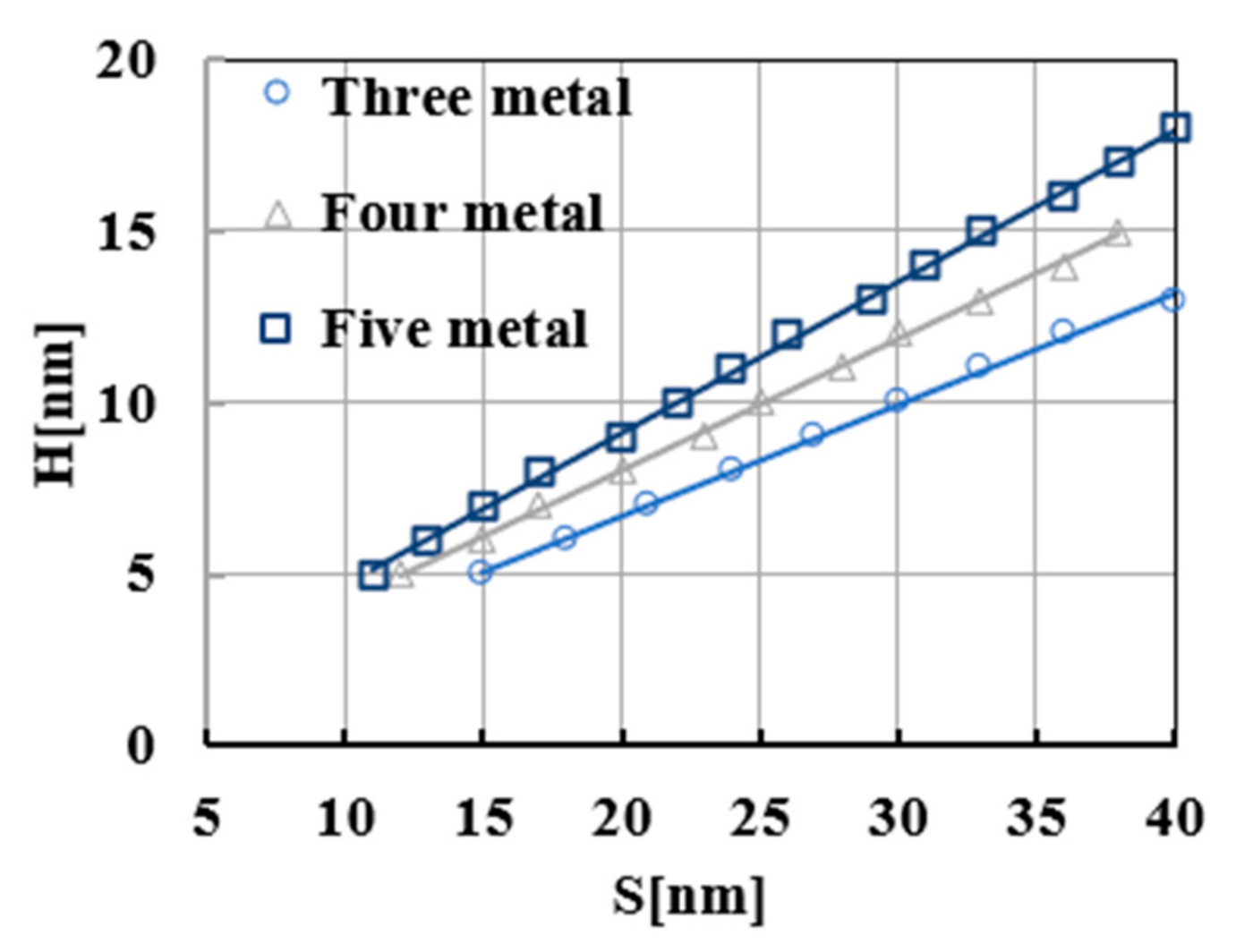
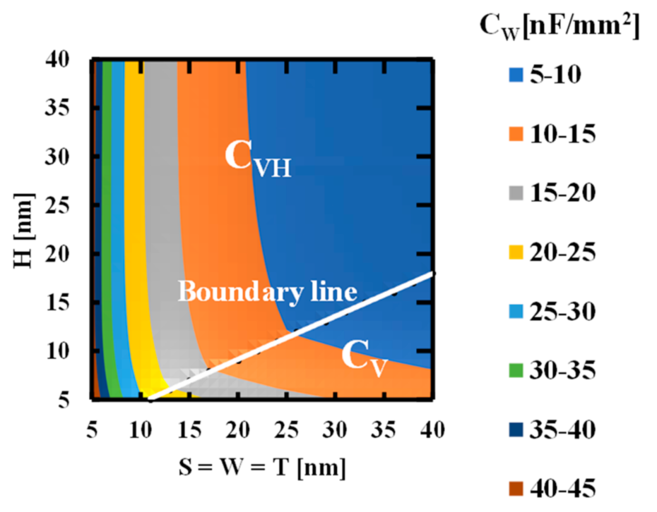
2.5. Scalability of Capacitance across 3D Crosspoint Memory Technology
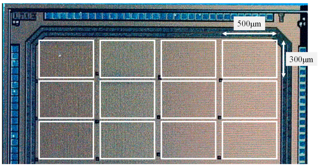
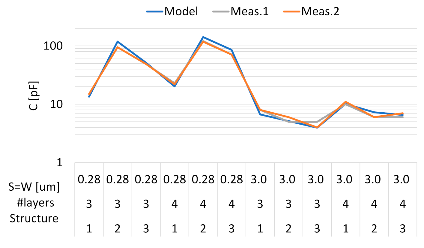
3. Measurement
4. Discussions
5. Conclusions
Author Contributions
Funding
Acknowledgments
Conflicts of Interest
Nomenclature
| W | Width of each wire |
| S | Space between wires |
| T | Thickness of wires |
| H | Height of dielectric film between levels of wires |
| CVER | Vertical capacitance component |
| CHOR | Horizontal capacitance component |
| CV | Vertical capacitor |
| CVH | Vertical and horizontal capacitors where even and odd numbers of wires are connected to the first and second terminals |
| CVH2 | Vertical and horizontal capacitors where two next neighbor wires are connected to the first and second terminals |
References
- Kau, D.C.; Tang, S.; Karpov, I.V.; Dodge, R.; Klehn, B.; Kalb, J.A.; Strand, J.; Diaz, A.; Leung, N.; Wu, J.; et al. A stackable cross point phase change memory. In Proceedings of the 2009 IEEE International Electron Devices Meeting (IEDM), Baltimore, MD, USA, 7 December 2009; pp. 1–4. [Google Scholar] [CrossRef]
- Kim, T.; Choi, H.; Kim, M.; Yi, J.; Kim, D.; Cho, S.; Lee, H.; Hwang, C.; Hwang, E.R.; Song, J.; et al. High-performance, cost-effective 2z nm two-deck crosspoint memory integrated by self-align scheme for 128 Gb SCM. In Proceedings of the 2018 IEEE International Electron Devices Meeting (IEDM), San Francisco, CA, USA, 1–5 December 2018; pp. 37.1.1–37.1.4. [Google Scholar] [CrossRef]
- Chien, W.C.; Ho, H.Y.; Yeh, C.W.; Yang, C.H.; Cheng, H.Y.; Kim, W.; Kuo, I.T.; Gignac, L.M.; Lai, E.K.; Gong, N.; et al. Comprehensive scaling study on 3D cross-point PCM toward 1Znm node for SCM applications. In Proceedings of the 2019 Symposium on VLSI Technology, Kyoto, Japan, 9–14 June 2019; pp. 60–61. [Google Scholar] [CrossRef]
- Chevallier, C.J.; Siau, C.H.; Lim, S.F. A 0.13 µm 64 Mb multi-layered conductive metal-oxide memory. In Proceedings of the 2010 IEEE International Solid-State Circuits Conference (ISSCC), San Francisco, CA, USA, 7 February 2010; pp. 260–261. [Google Scholar] [CrossRef]
- Kawahara, A.; Azuma, R.; Ikeda, Y.; Kawai, K.; Katoh, Y.; Hayakawa, Y.; Tsuji, K.; Yoneda, S.; Himeno, A.; Shimakawa, K.; et al. An 8 Mb Multi-Layered Cross-Point ReRAM Macro With 443 MB/s Write Throughput. IEEE J. Solid-State Circuits 2013, 48, 178–185. [Google Scholar] [CrossRef]
- Yu, S.; Deng, Y.; Gao, B.; Huang, P.; Chen, B.; Liu, X.; Kang, J.; Chen, H.Y.; Jiang, Z.; Wong, H.S. Design Guidelines for 3D RRAM Cross-Point Architecture. In Proceedings of the IEEE International Symposium on Circuits and Systems (ISCAS), Melbourne, Australia, 1 June 2014; pp. 421–424. [Google Scholar] [CrossRef]
- Zhou, J.; Kim, K.H.; Lu, W. Crossbar RRAM Arrays: Selector Device Requirements during Read Operation. IEEE Trans. Electron Devices 2014, 61, 1369–1376. [Google Scholar] [CrossRef]
- Chiu, P.-F.; Nikoli, B. A differential 2R crosspoint RRAM array with zero standby current. IEEE Trans. Circuits Syst. II Exp. Briefs 2015, 62, 461–465. [Google Scholar] [CrossRef]
- Andersen, T.M.; Krismer, F.; Kolar, J.W.; Toifl, T.; Menolfi, C.; Kull, L.; Morf, T.; Kossel, M.; Brändli, M.; Buchmann, P.; et al. A sub-ns response on-chip switched-capacitor DC-DC voltage regulator delivering 3.7 W/mm2 at 90% efficiency using deep-trench capacitors in 32nm SOI CMOS. In Proceedings of the IEEE International Solid-State Circuits Conference Digest of Technical Papers (ISSCC), San Francisco, CA, USA, 9–13 February 2014. [Google Scholar] [CrossRef]
- Pei, C.; Booth, R.; Ho, H.; Kusaba, N.; Li, X.; Brodsky, M.; Parries, P.; Shang, H.; Divakaruni, R.; Iyer, S. A novel, low-cost deep trench decoupling capacitor for high-performance, low-power bulk CMOS applications. In Proceedings of the International Conference on Solid-State and Integrated-Circuit Technology, Beijing, China, 20–23 October 2008; pp. 1146–1149. [Google Scholar] [CrossRef]
- El-Damak, D.; Bandyopadhyay, S.; Chandrakasan, A.P. A 93% Efficiency Reconfigurable Switched-Capacitor DC-DC Converter Using On-Chip Ferroelectric Capacitors. In Proceedings of the IEEE International Solid-State Circuits Conference Digest of Technical Papers, San Francisco, CA, USA, 17–21 February 2013; pp. 374–375. [Google Scholar] [CrossRef] [Green Version]
- Tanzawa, T.; Murakoshi, T.; Kamijo, T.; Tanaka, T.; McNeil, J.J.; Duesman, K. Design challenge in 3D NAND technology: A 4.8X area- and 1.3X power-efficient 20V charge pump using tier capacitors. In Proceedings of the IEEE Asian Solid-State Circuits Conference, Toyama, Japan, 7–9 November 2016; pp. 165–168. [Google Scholar] [CrossRef]
- Somasekhar, D.; Srinivasan, B.; Pandya, G.; Hamzaoglu, F.; Khellah, M.; Karnik, T.; Zhang, K. Multi-phase 1GHz voltage doubler charge-pump in 32nm logic process. IEEE J. Solid-State Circuits 2010, 45, 751–758. [Google Scholar] [CrossRef]
- Tanzawa, T. On-chip switched-capacitor DC-DC converter in memory technology: State of the art and challenges. In Proceedings of the European Conference on Circuit Theory and Design (ECCTD), Catania, Italy, 4–6 September 2017. [Google Scholar] [CrossRef]
- Ruehli, A.; Brennan, P.A. Capacitance models for integrated circuit metallization wires. IEEE J. Solid-State Circuits 1975, 10, 530–536. [Google Scholar] [CrossRef]
- Arora, N.D.; Raol, K.V.; Schumann, R.; Richardson, L.M. Modeling and extraction of interconnect capacitances for multilayer VLSI circuits. IEEE Trans. Comput.-Aided Des. Integr. Circuits Syst. 1996, 15, 58–67. [Google Scholar] [CrossRef]
- Wong, S.C.; Liu, P.S.; Ru, J.W.; Lin, S.T. Interconnection capacitance models for VLSI circuits. Solid-State Electron. 1998, 42, 969–977. [Google Scholar] [CrossRef]
- Wong, S.C.; Lee, T.G.Y.; Ma, D.J.; Chao, C.J. An Empirical Three-Dimensional Crossover Capacitance Model for Multilevel Interconnect VLSI Circuits. IEEE Trans. Semicond. Manuf. 2000, 13, 219–227. [Google Scholar] [CrossRef]
- Aparicio, R.; Hajimiri, A. Capacity limits and matching properties of integrated capacitors. IEEE J. Solid-State Circuits 2002, 37, 384–393. [Google Scholar] [CrossRef]


| CVER (Figure 4a) | CHOR (Figure 4c) | |
|---|---|---|
| CV (Figure 3a) | (M − 1) N2 | None |
| CVH (Figure 3b) | (M − 1 N2/2 | M (Ch1 N (N − 1) + Ch2 (N − 1)2) |
| CVH2 (Figure 3c) | (M − 1 N2/2 | M (Ch1 N/2 (N − 1) + Ch2 (N/2 − 1) (N − 1)) |
| 1 | 2 | 3 | 4 | 5 | 6 | 7 | 8 | 9 | 10 | 11 | 12 | |
|---|---|---|---|---|---|---|---|---|---|---|---|---|
| S = W [µm] | 0.28 µm | 3.0 µm | ||||||||||
| # wires | 3 | 4 | 3 | 4 | ||||||||
| C structure | CV | CVH | CVH2 | CV | CVH | CVH2 | CV | CVH | CVH2 | CV | CVH | CVH2 |
Publisher’s Note: MDPI stays neutral with regard to jurisdictional claims in published maps and institutional affiliations. |
© 2021 by the authors. Licensee MDPI, Basel, Switzerland. This article is an open access article distributed under the terms and conditions of the Creative Commons Attribution (CC BY) license (https://creativecommons.org/licenses/by/4.0/).
Share and Cite
Tone, Y.; Tanzawa, T. An Optimum Structure of Scalable Capacitors in 3D Crosspoint Memory Technology. Electronics 2021, 10, 2755. https://doi.org/10.3390/electronics10222755
Tone Y, Tanzawa T. An Optimum Structure of Scalable Capacitors in 3D Crosspoint Memory Technology. Electronics. 2021; 10(22):2755. https://doi.org/10.3390/electronics10222755
Chicago/Turabian StyleTone, Yuya, and Toru Tanzawa. 2021. "An Optimum Structure of Scalable Capacitors in 3D Crosspoint Memory Technology" Electronics 10, no. 22: 2755. https://doi.org/10.3390/electronics10222755