
Modeling of Average Current in Non-Ideal Buck and Synchronous Buck Converters for Low Power Application


Abstract
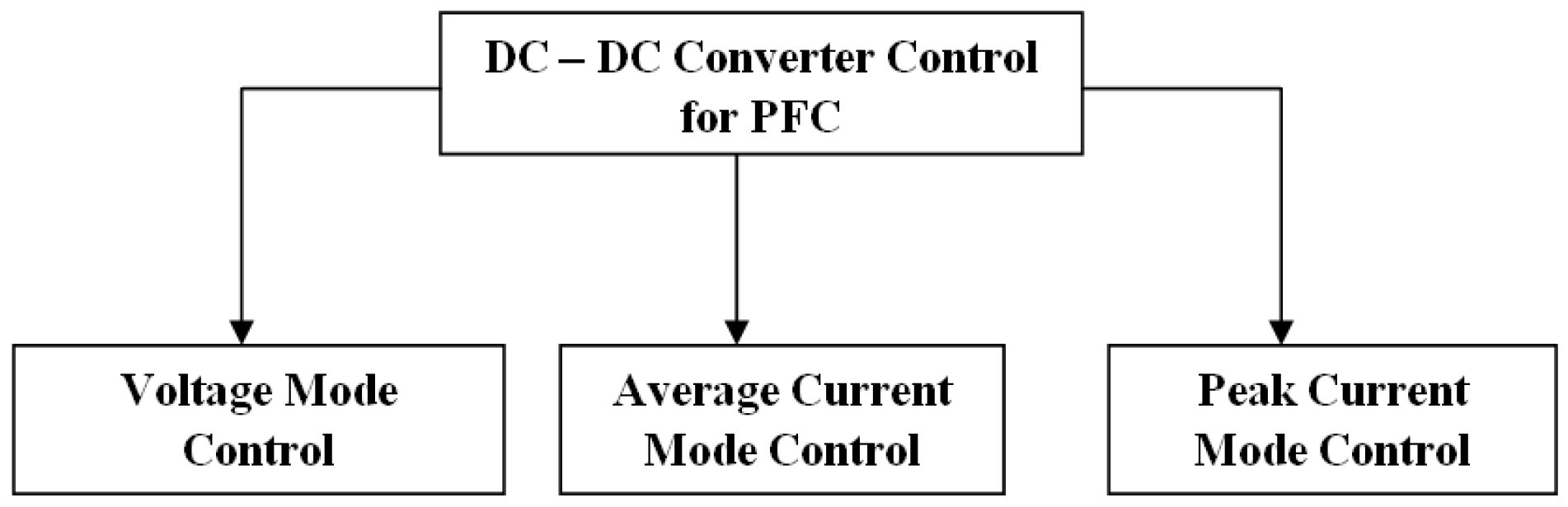
:1. Introduction
- The existing works featured on steady-state and transient performance analysis of the DC–DC ideal and non-ideal converters for low-power application based on the specifications shown in [11].
- The Gid for a current loop is considered. However, the outer voltage loop is not taken into account.
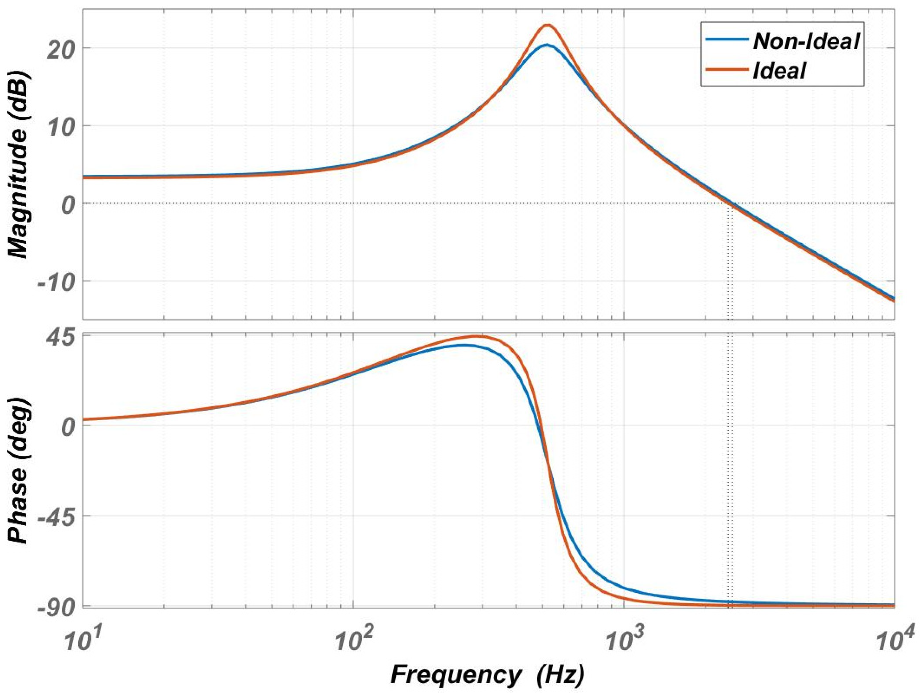
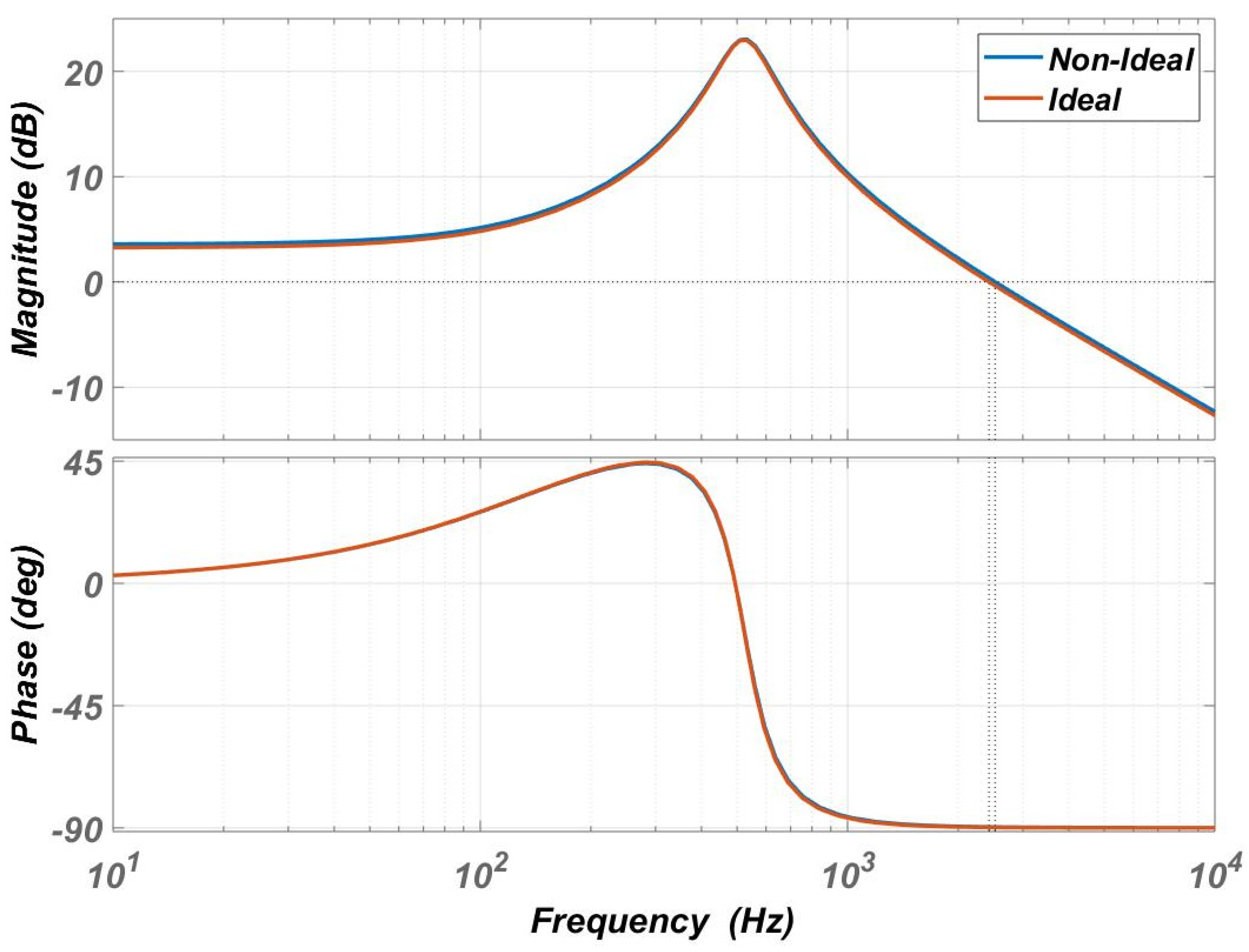
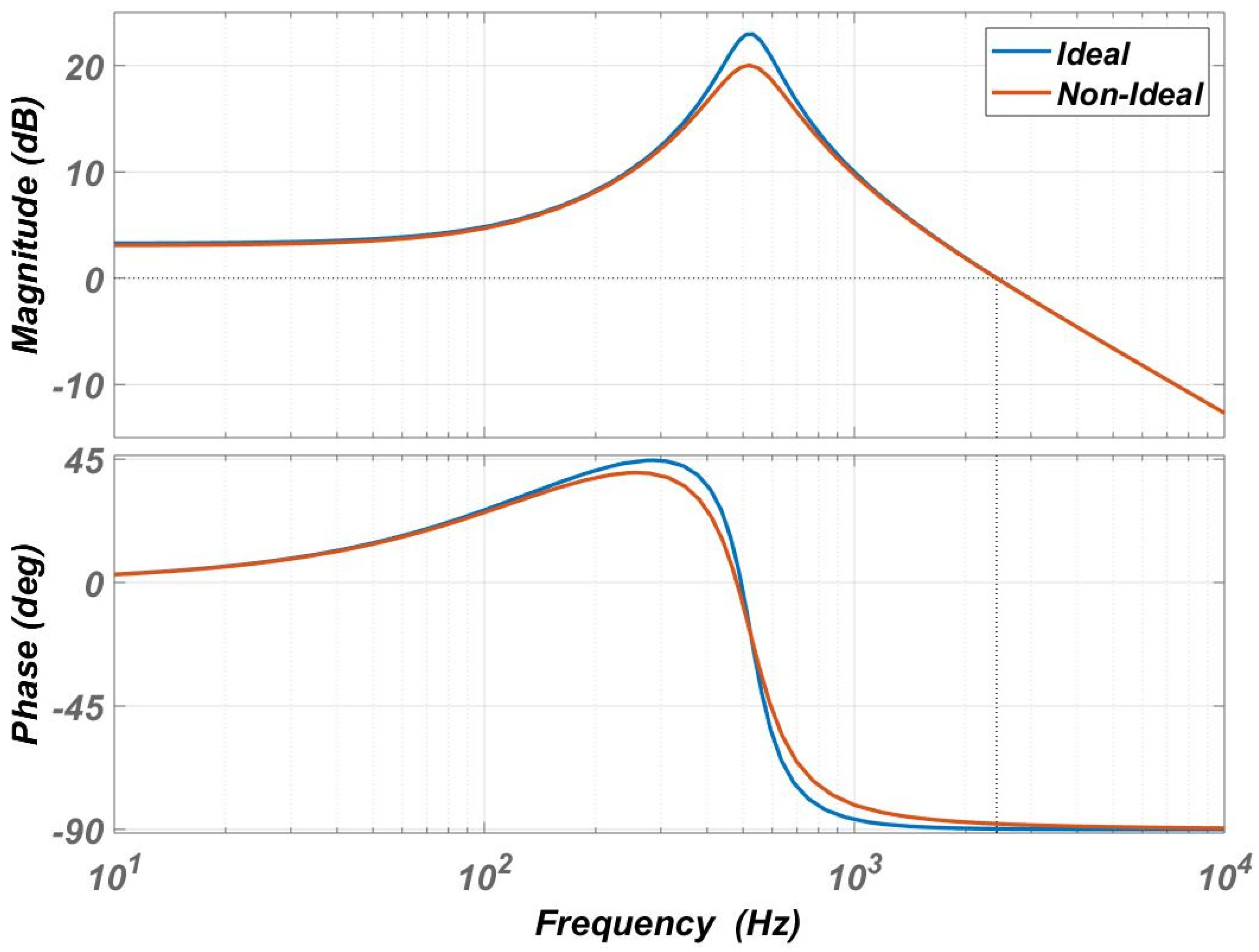
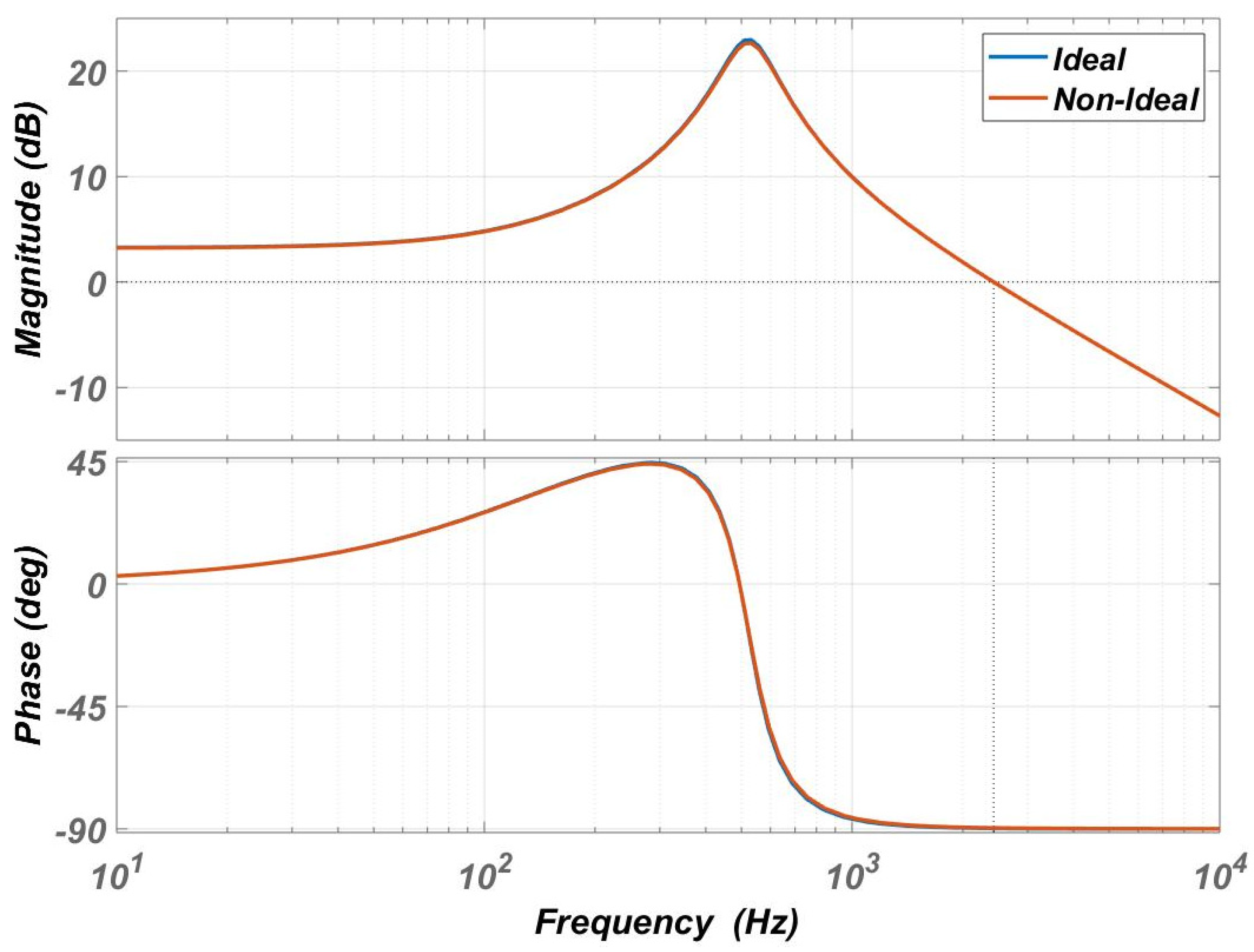
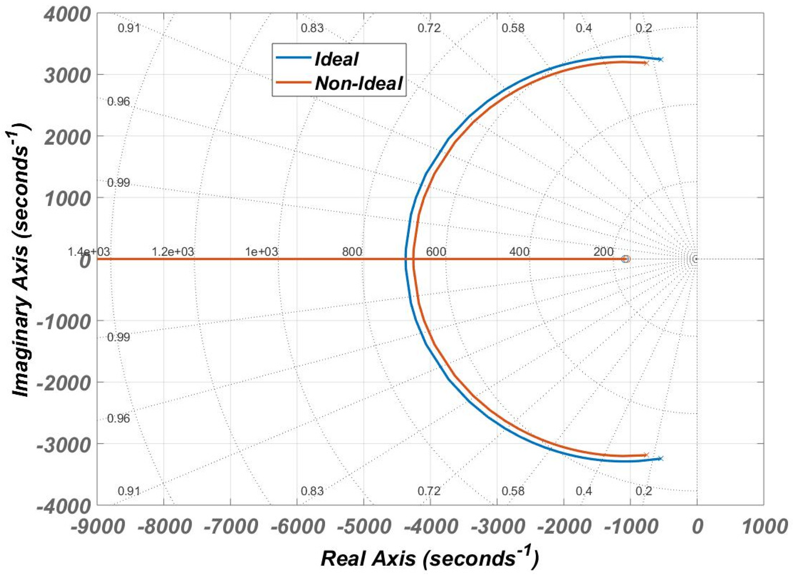
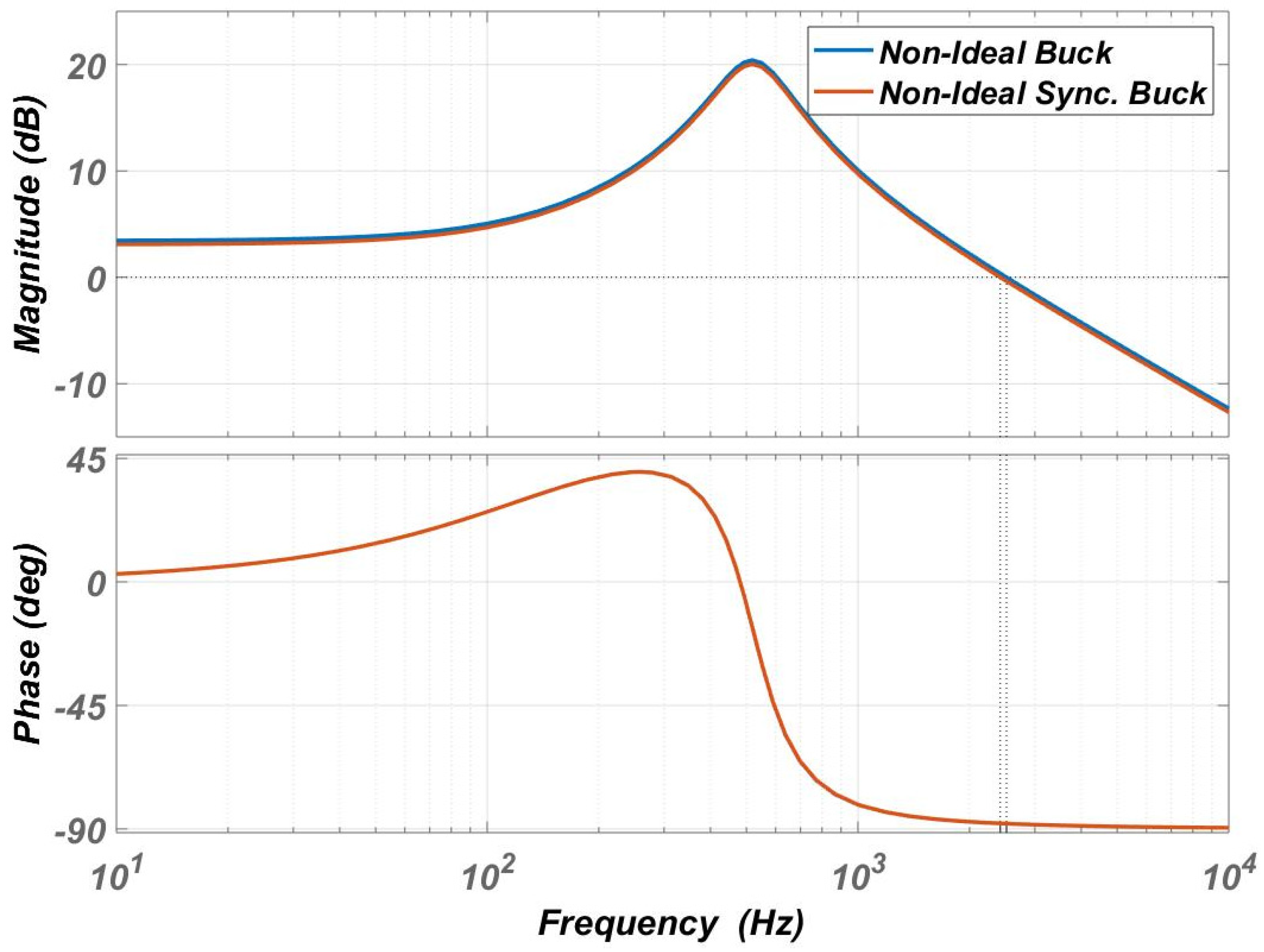
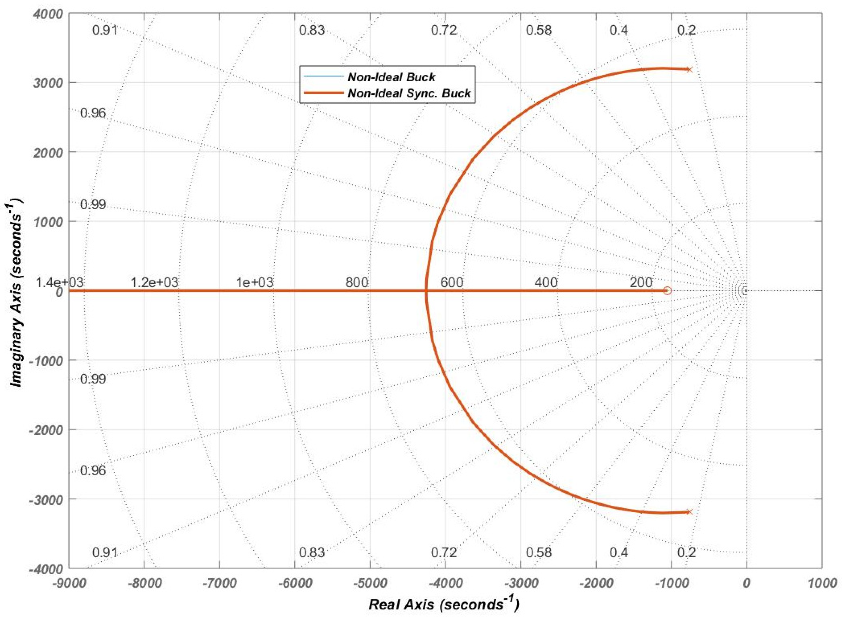
- The Gid of a non-ideal buck converter was compared with a non-ideal synchronous buck converter. Sensitivity analysis of the Gid was carried out by analyzing the bode plots for varying ESR.
- The modeling of the converters was presented considering all the non-idealities such as the switch and diode resistances and ESRs of inductor and capacitor.
- However, very few works have focused on the mathematical modeling of the average current control strategy for the same.
- The average current model for ideal and non-ideal buck and synchronous buck converters is modeled using the SSA technique.
- The emphasis is on modeling the Gid and observations are made on low frequency gain, crossover frequency, resonant frequency, location of poles and zeros, and gain and phase margins.
- The objective of the work is to aid the understanding and significance of mathematical modeling and the effect of the Gid on this proposed strategy and its significance in stability and control.
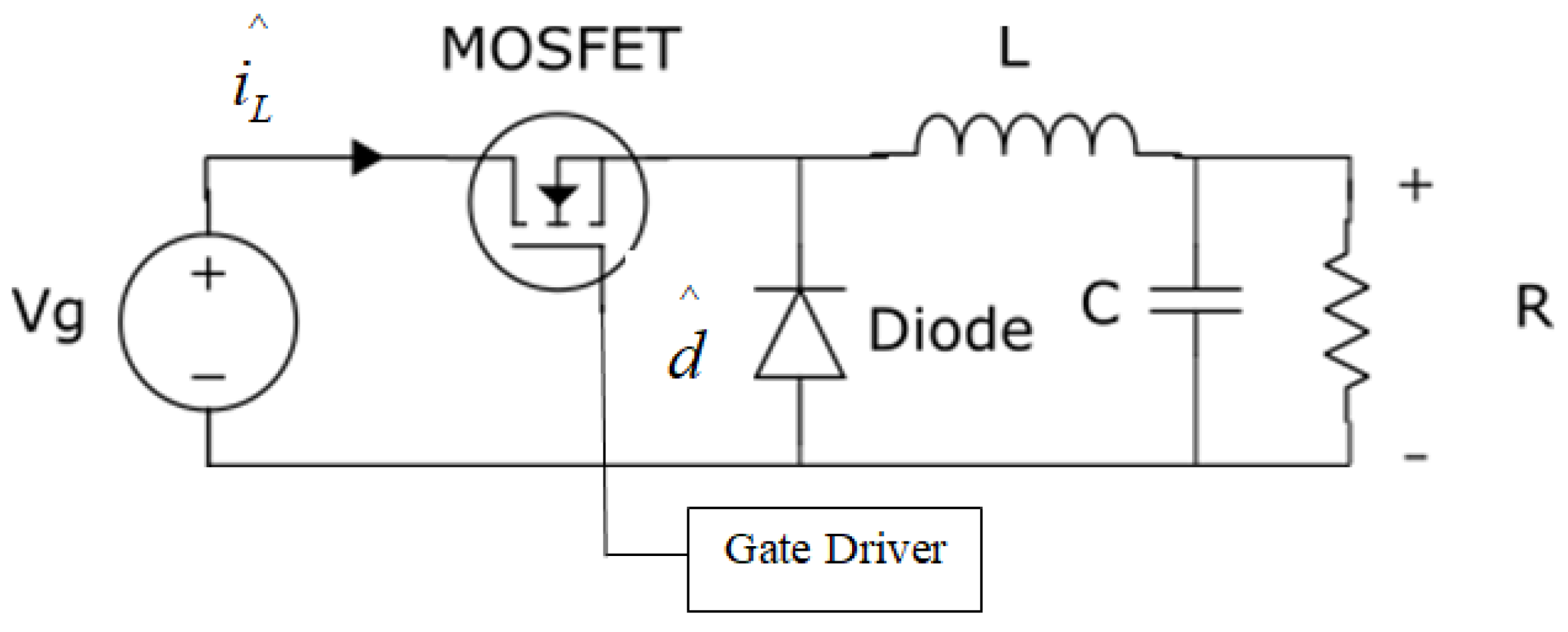
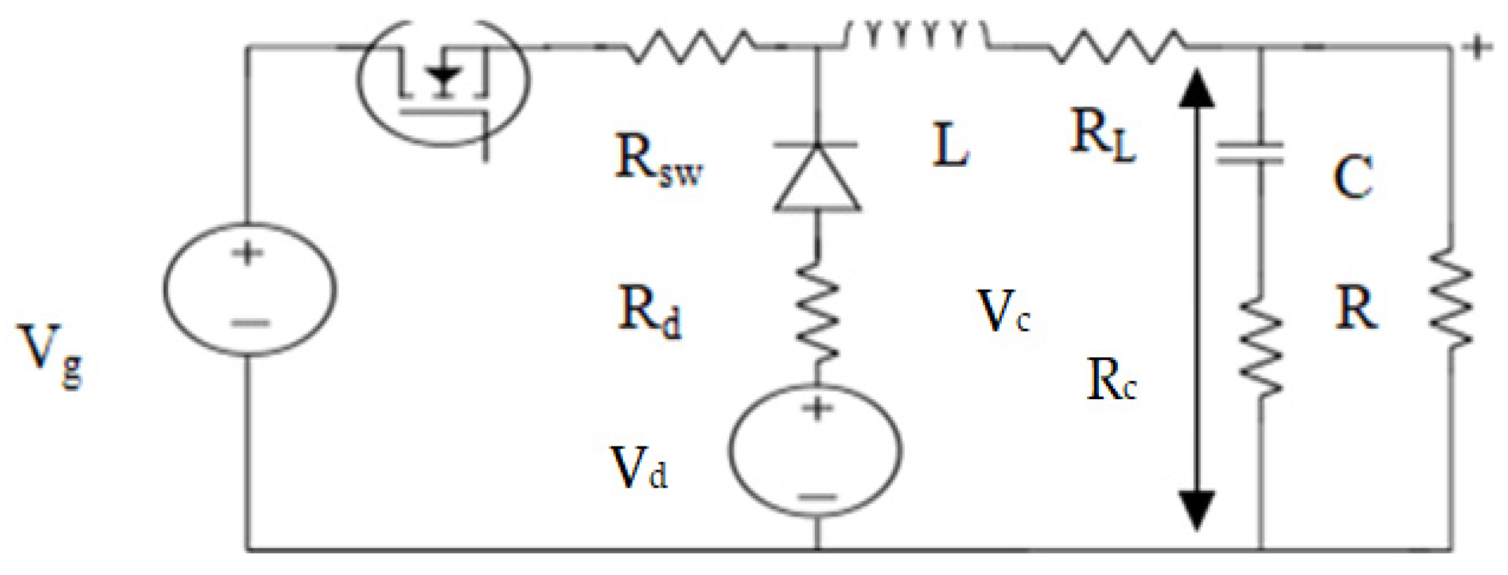
2. Average Current Modeling in Non-Ideal Buck Converter
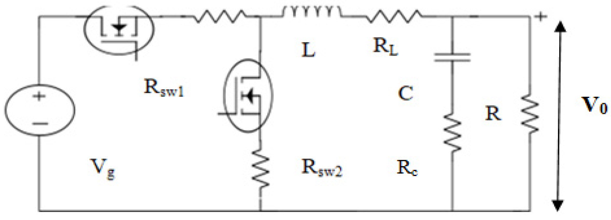
3. Average Current Modeling in Non-Ideal Synchronous Buck Converter
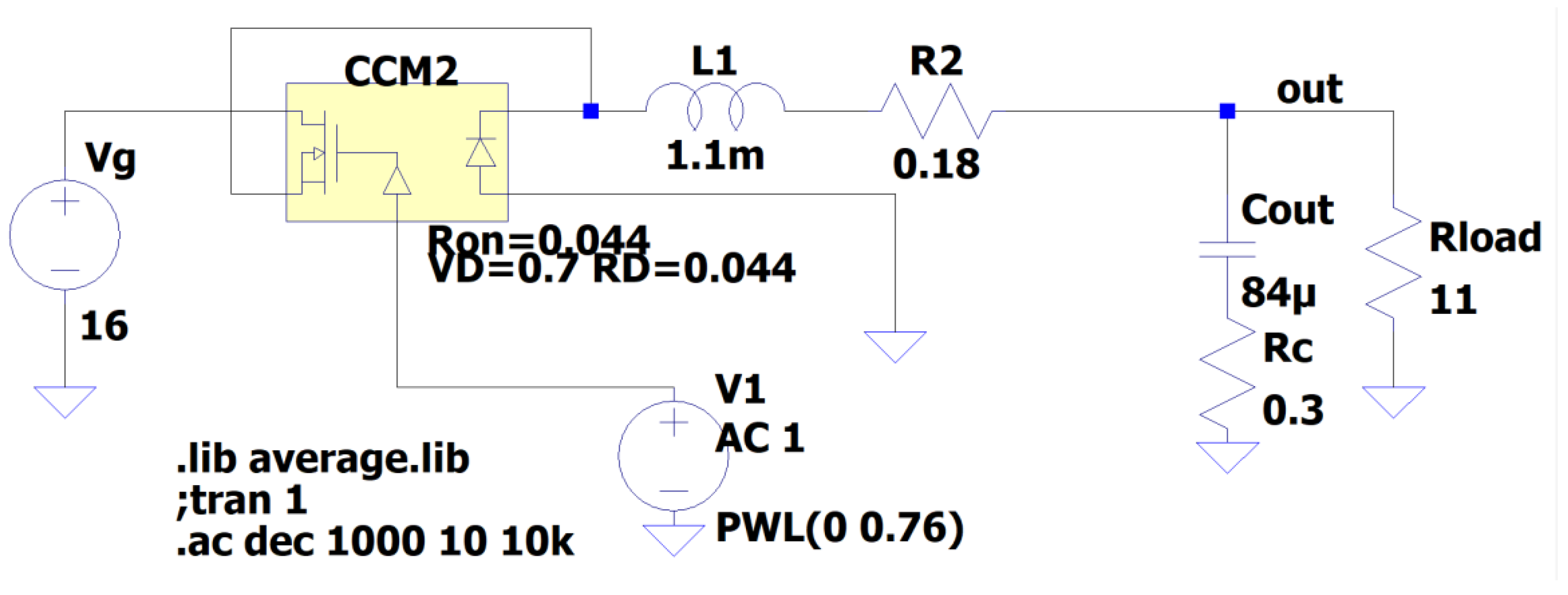
4. Specifications of the converter
5. Mathematical Modeling of the Converters
6. Results of ACC in Open Loop Configuration
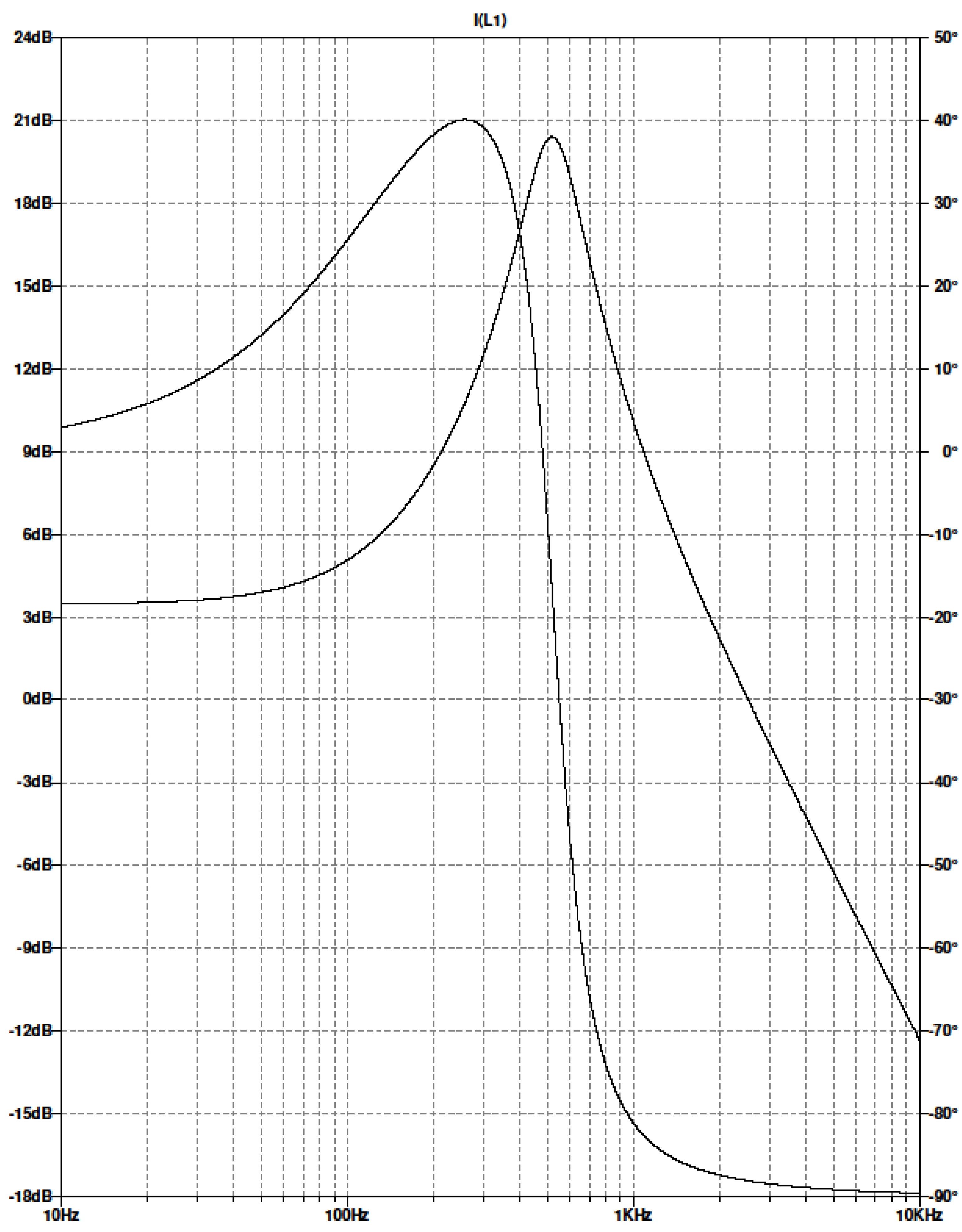
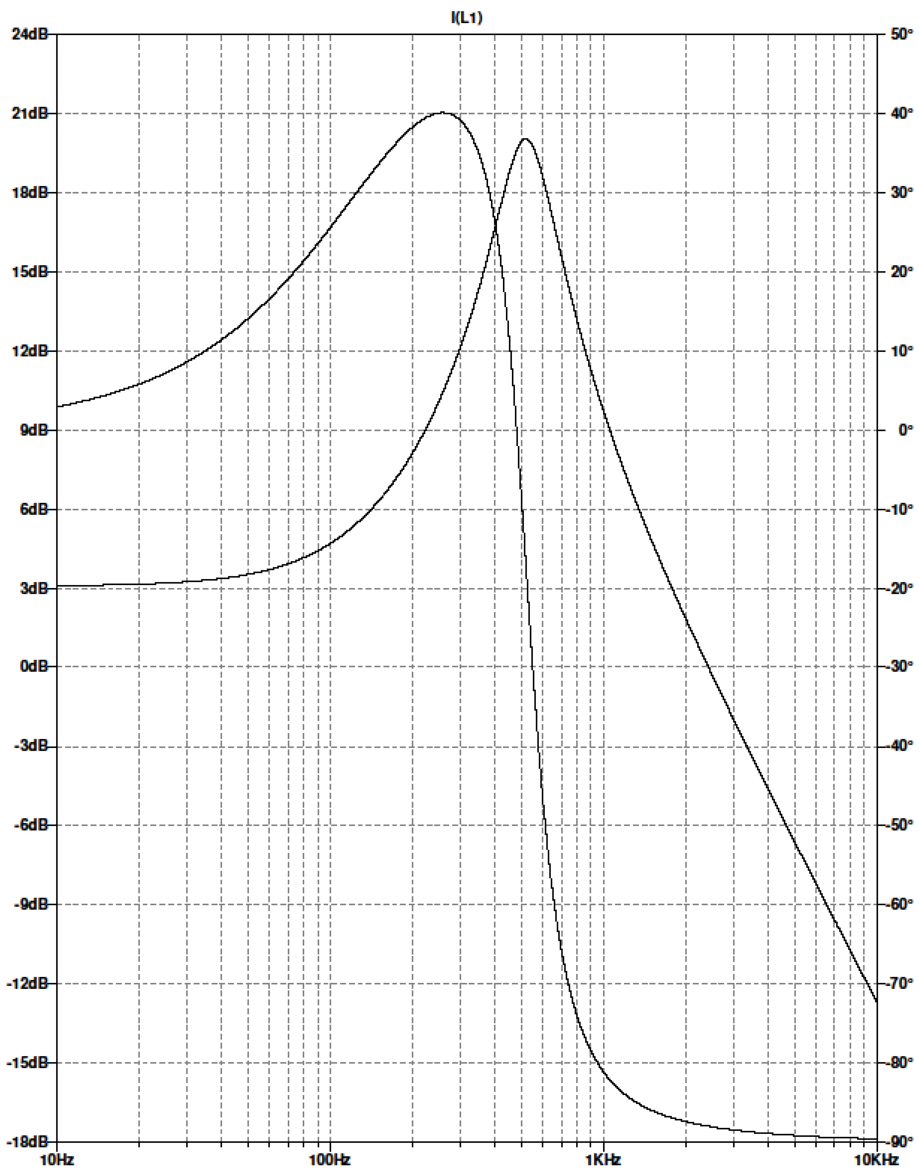
7. Validation Using LTspice
8. Conclusions
- ACC modeling for ideal and non-ideal buck and synchronous buck converters operating in CCM is carried out from basic equations of volt-sec and amp-second balance equations for a single current loop.
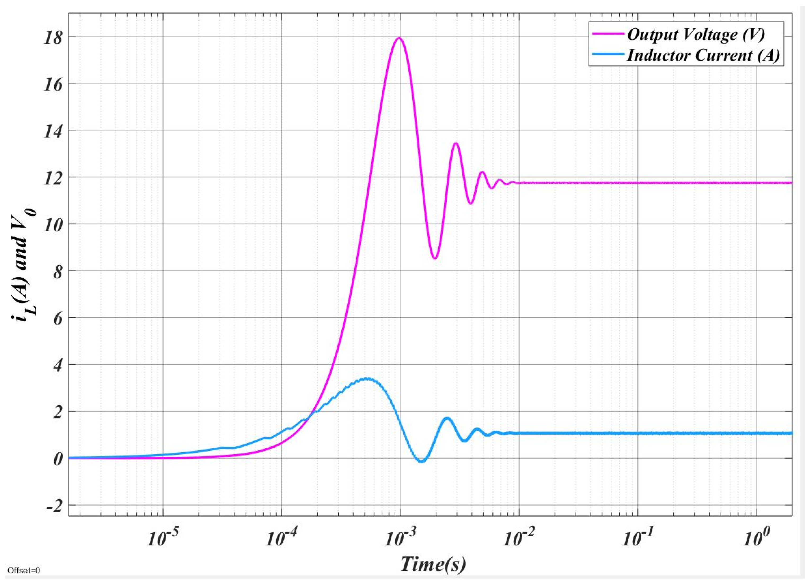
- The converters were initially modeled using volt-sec and amp-sec balance equations. Using MATLAB/Simulink software, the mathematical model was analyzed and the transients in output voltage and inductor current were clearly seen.
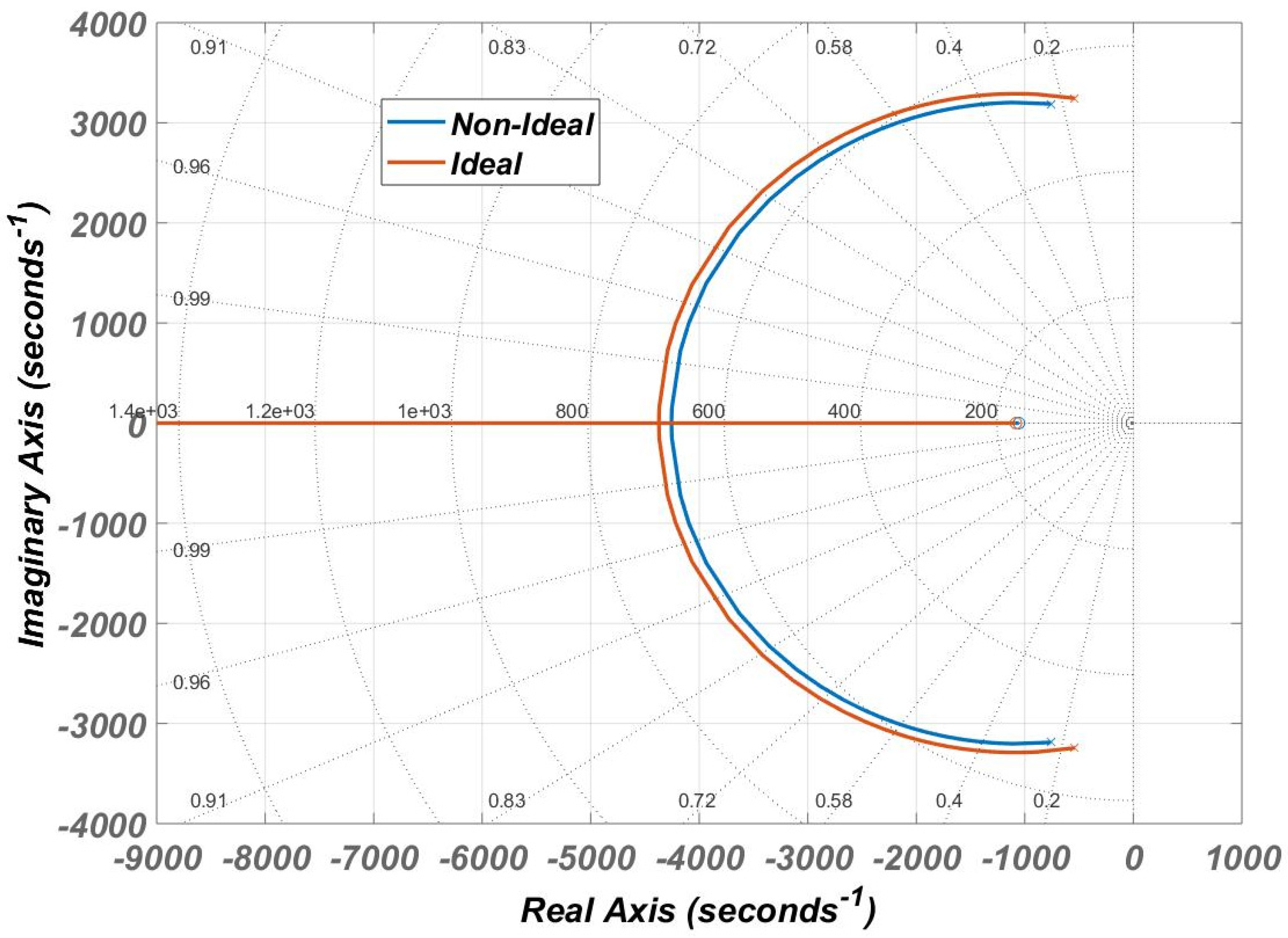
- Later, using the state space averaging technique, the average current transfer function Gid was derived for the ideal and non-ideal converters.
- The ideal and non-ideal converters were highly stable. However, the ideal buck converter showed higher resonant frequency than the non-ideal converter. This is due to the presence of ESRs in the inductor and the capacitor. A similar phenomenon was observed in ideal and non-synchronous converters.
- The derived transfer function was validated against standard switch models using the LTspice software. The plots show a perfect match between the derived transfer function and the actual switch model.
- The ACC modeling with closed loop control is to be carried out for different converter CCM/DCM configurations with inner current and outer voltage loops, and the effect of the capacitor ESR in the closed loop configuration is to be analyzed. The input current and the voltage can be controlled in order to achieve a power factor close to unity.
Author Contributions
Funding
Conflicts of Interest
References
- Middlebrook, R.D. Modeling current-programmed buck and boost regulators. IEEE Trans. Power Electron. 1989, 4, 36–52. [Google Scholar] [CrossRef] [Green Version]
- Sun, C.; Lehman, B. Modeling of Average Current Mode Control in PWM DC/DC Converters. IFAC Proc. Vol. 1999, 32, 7421–7426. [Google Scholar] [CrossRef]
- Erickson, R.W.; Maksimovic, D. Fundamentals of Power Electronics; Springer Science & Business Media: Berlin, Germany, 2007. [Google Scholar]
- Sumukh, S.; Surpiya, P.; Williamson, S. A Comprehensive Study on DC–DC and DC–AC Converters in Electric and Hybrid Electric Vehicles. In Accepted for Publication E-Mobility—A New Era in Automotive Technology; Springer: Berlin/Heidelberg, Germany, 2021. [Google Scholar]
- Sharifi, S.; Babaei, M.; Monfared, M. A high gain buck PFC synchronous rectifier. In Proceedings of the Electrical Engineering (ICEE), Iranian Conference on, Mashhad, Iran, 8–10 May 2018; IEEE: Piscataway, NJ, USA, 2018. [Google Scholar]
- Channappanavar, R.; Mishra, S.K.; Singh, R.K. An inductor current estimator for digitally controlled synchronous buck converter. IEEE Trans. Power Electron. 2018, 34, 4883–4894. [Google Scholar] [CrossRef]
- Surya, S.; Arjun, M.N. Mathematical Modeling of Power Electronic Converters. SN Comput. Sci. 2021, 2, 1–9. [Google Scholar] [CrossRef]
- Surya, S.; Williamson, S. Generalized circuit averaging technique for two-switch PWM DC-DC converters in CCM. Electronics 2021, 10, 392. [Google Scholar] [CrossRef]
- Chakraborty, S.; Hasan, M.M.; Worighi, I.; Hegazy, O.; Razzak, M.A. Performance evaluation of a PID-controlled synchronous buck converter based battery charging controller for solar-powered lighting system in a fishing trawler. Energies 2018, 11, 2722. [Google Scholar] [CrossRef] [Green Version]
- Surya, S.; Channegowda, J.; Naraharisetti, K. Generalized Circuit Averaging Technique for Two Switch DC-DC Converters. In Proceedings of the 2020 8th International Conference on Power Electronics Systems and Applications (PESA), Hong Kong, China, 7–10 December 2020; IEEE: Piscataway, NJ, USA, 2020. [Google Scholar]
- Garg, M.M.; Pathak, M.K. Performance comparison of non-ideal and ideal models of DC-DC Buck converter. In Proceedings of the 2018 8th IEEE India International Conference on Power Electronics (IICPE), Jaipur, India, 13–15 December 2018; IEEE: Piscataway, NJ, USA, 2018. [Google Scholar]
- Surya, S.; Williamson, S. Modeling of Average Current in Ideal and Non-Ideal Boost and Synchronous Boost Converters. Energies 2021, 14, 5118. [Google Scholar] [CrossRef]
- Chou, H.H.; Chen, H.L. A Novel Buck Converter with Constant Frequency Controlled Technique. Energies 2021, 14, 5911. [Google Scholar] [CrossRef]
- Granda, M.; Fernandez, C.; Barrado, A.; Zumel, P. Nonparametric Frequency Response Identification for Dc-Dc Converters Based on Spectral Analysis with Automatic Determination of the Perturbation Amplitude. Sensors 2021, 21, 3234. [Google Scholar] [CrossRef] [PubMed]
- Lin, B.-R.; Goh, A.P.I.; Wang, K.-W. Analysis of a Resonant Converter with Wide Input Voltage. Electronics 2021, 10, 1110. [Google Scholar] [CrossRef]
- Tai, L.; Lin, M.; Wang, J.; Hou, C. Synchronous Control Strategy with Input Voltage Feedforward for a Four-Switch Buck-Boost Converter Used in a Variable-Speed PMSG Energy Storage System. Electronics 2021, 10, 2375. [Google Scholar] [CrossRef]
- Cuoghi, S.; Mandrioli, R.; Ntogramatzidis, L.; Gabriele, G. Multileg Interleaved Buck Converter for EV Charging: Discrete-Time Model and Direct Control Design. Energies 2020, 13, 466. [Google Scholar] [CrossRef] [Green Version]
- Xie, H.; Guo, E. How the Switching Frequency Affects the Performance of a Buck Converter. Available online: https://www.ti.com/lit/an/slvaed3/slvaed3.pdf?ts=1635120058978&ref_url=https%253A%252F%252Fwww.google.co.in%252F (accessed on 25 October 2021).
- Available online: https://www.onsemi.cn/pub/collateral/tnd352-d.pdf (accessed on 25 October 2021).
- Rahimi, B.A.M.; Parto, P.; Asadi, P. Compensator Design Procedure for Buck Converter with Voltage-Mode Error-Amplifier. Available online: https://www.infineon.com/dgdl/an-1162.pdf?fileId=5546d462533600a40153559a8e17111a (accessed on 25 October 2021).
- Available online: https://www.ti.com/seclit/ml/slup341/slup341.pdf (accessed on 25 October 2021).
- Priewasser, R.; Agostinelli, M.; Unterrieder, C.; Marsili, S.; Huemer, M. Modeling, control, and implementation of DC–DC converters for variable frequency operation. IEEE Trans. Power Electron. 2014, 29, 287–301. [Google Scholar] [CrossRef]
- Lionel, F.D.J.; Dias, J.; Srinivasan, M.K.; Parandhaman, B.; Prabhakaran, P. A Novel Non-Isolated Dual-Input DC-DC Boost Converter for Hybrid Electric Vehicle Application. Int. J. Emerg. Electr. Power Syst. 2021, 22, 191–204. [Google Scholar]
- Sreelakshmi, S.; Krishna, M.; Deepa, K. Bidirectional Converter Using Fuzzy for Battery Charging of Electric Vehicle. In Proceedings of the 2019 IEEE Transportation Electrification Conference (ITEC-India), Bengaluru, India, 17–19 December 2019. [Google Scholar]
- Lionel, F.D.J.; Jayan, J.; Srinivasan, M.K.; Prabhakaran, P. DC-Link Current Based Position Estimation and Speed Sensorless Control of a BLDC Motor Used for Electric Vehicle Applications. Int. J. Emerg. Electr. Power Syst. 2021, 22, 269–284. [Google Scholar]
- Surya, S.; Srinivasan, M.K.; Williamson, S. Technological Perspective of Cyber Secure Smart Inverters Used in Power Distribution System: State of the Art Review. Appl. Sci. 2021, 11, 8780. [Google Scholar] [CrossRef]
- Surya, S.; Singh, D.B. Comparative study of P, PI, PD and PID controllers for operation of a pressure regulating valve in a blow-down wind tunnel. In Proceedings of the 2019 IEEE International Conference on Distributed Computing, VLSI, Electrical Circuits and Robotics (DISCOVER), Manipal, India, 11–12 August 2019. [Google Scholar]


| SL.NO | Specifications | Value |
|---|---|---|
| 1 | Input Voltage, Vg | 16 V |
| 2 | Output Voltage, V0 | 12 V |
| 3 | Output Resistance, R | 11 Ω |
| 4 | Inductance, L | 1.1 mH |
| 5 | Inductor ESR, RL | 0.18 Ω |
| 6 | Capacitance, C | 84 µF |
| 7 | Capacitor ESR, Rc | 0.3 Ω |
| 8 | Switch Resistance, Rsw | 0.044 Ω |
| 9 | Diode Resistance, Rd | 0.024 Ω |
| 10 | Diode Forward Voltage, Vd | 0.7 V |
| 11 | Duty Cycle, D | 0.75 |
| 12 | Switching Frequency, fs | 25 kHz |
Publisher’s Note: MDPI stays neutral with regard to jurisdictional claims in published maps and institutional affiliations. |
© 2021 by the authors. Licensee MDPI, Basel, Switzerland. This article is an open access article distributed under the terms and conditions of the Creative Commons Attribution (CC BY) license (https://creativecommons.org/licenses/by/4.0/).
Share and Cite
Surya, S.; Srinivasan, M.K.; Williamson, S. Modeling of Average Current in Non-Ideal Buck and Synchronous Buck Converters for Low Power Application. Electronics 2021, 10, 2672. https://doi.org/10.3390/electronics10212672
Surya S, Srinivasan MK, Williamson S. Modeling of Average Current in Non-Ideal Buck and Synchronous Buck Converters for Low Power Application. Electronics. 2021; 10(21):2672. https://doi.org/10.3390/electronics10212672
Chicago/Turabian StyleSurya, Sumukh, Mohan Krishna Srinivasan, and Sheldon Williamson. 2021. "Modeling of Average Current in Non-Ideal Buck and Synchronous Buck Converters for Low Power Application" Electronics 10, no. 21: 2672. https://doi.org/10.3390/electronics10212672