Article

Effects of Chamber Pressures on the Passivation Layer of Hydrogenated Nano-Crystalline Silicon Mixed-Phase Thin Film by Using Microwave Annealing

1
Department of Electronic Engineering, National Kaohsiung University of Science and Technology, Kaohsiung 807618, Taiwan
2
Department of Electrical Engineering, Feng Chia University, Taichung 407802, Taiwan
3
Micro Nano System Center, School of Information Science and Technology, Fudan University, Shanghai 200433, China
4
Opto-Electronics Technology Section Energy and Agile System Department, Metal Industries Research & Development Centre, Kaohsiung 821011, Taiwan
5
Institute of Photonics Engineering, National Kaohsiung University of Science and Technology, Kaohsiung 807618, Taiwan
*
Author to whom correspondence should be addressed.
Electronics 2021, 10(18), 2199; https://doi.org/10.3390/electronics10182199
Submission received: 9 August 2021 / Revised: 30 August 2021 / Accepted: 4 September 2021 / Published: 8 September 2021
(This article belongs to the Special Issue Advanced Design of RF/Microwave Circuit)

Abstract

:
This paper proposes the effects of chamber pressures on the passivation layer of hydrogenated nano-crystalline silicon (nc-Si:H) mixed-phase thin film using microwave annealing (MWA) to achieve a high-quality thin film. The use of 40.68 MHz very-high-frequency plasma-enhanced chemical vapor deposition (VHFPECVD) deposited the nc-Si:H mixed-phase thin film on the top and bottom of the n-type crystalline silicon substrate. The chamber pressures (0.2, 0.4, 0.6, and 0.8 Torr) of the VHFPECVD were critical factors in controlling the carrier lifetime of the symmetric structure. By using the VHFPECVD to deposit the nc-Si:H and using the MWA to enhance the quality of the symmetric structure, the deposited nc-Si:H’s properties of a crystalline volume fraction of 29.6%, an optical bandgap of 1.744 eV, and a carrier lifetime of 2942.36 μs were well achieved, and could be valuable in thin-film solar-cell applications.

1. Introduction

Thin-film solar cells are being increasingly adopted as a pollution-free power source. Current research is focused on high-efficiency solar cells. Surface passivation is crucial for achieving high-conversion-efficiency crystalline silicon solar cells [1]. The passivation layer deposition is an essential process step in developing crystalline silicon (c-Si) solar cells [2]. Some studies reported the deposition of hydrogenated nano-crystalline silicon (nc-Si:H) passivation layer thin films [3,4,5,6,7]. The nc-Si:H thin film shows much promise in the application of solar cells due to good features such as a tunable bandgap (1.1 to 3 eV), high optical absorption (>104 cm−1), and better carrier mobility (~103 cm2/V s) [8,9,10,11]. The growing methods of nc-Si:H film typically are plasma-enhanced chemical vapor deposition (PECVD) [12], radio-frequency (RF) sputtering [13], and hot-wire chemical vapor deposition (HWCVD) [14].
The use of very-high-frequency PECVD (VHFPECVD) has several advantages, such as high plasma density (>1.0 × 1010 cm−3) and reduced ionic bombardment (energy of about 10–100 eV) [15,16,17,18,19]. It was reported that a high deposition rate (>4 Å/s) and high pressure (>0.1 Torr) of VHFPECVD are effective for growing high-quality µc-Si:H films [20,21,22,23,24]. However, when using hot-wire chemical vapor deposition, the radiant heat of the filaments leads to a substantial increase of the substrate temperatures, limiting the deposition rate for high-quality thin films [25]. Therefore, VHFPECVD at 40.68 MHz is a preferred method for mixed-phase (a combination of amorphous and nano-crystalline) silicon thin-film deposition on crystalline silicon wafer substrates.
The annealing process plays a crucial role in obtaining a high carrier lifetime in the hydrogenation from the film to the c-Si surface. Some studies related to post-annealing have been reported [26,27,28,29,30]. Microwave annealing (MWA) is a new and effective method to obtain high-carrier-lifetime thin films. The effects are ascribed to the details of microwave absorption, which selectively affects Si–H bonds, and thus hydrogen bonds were restructured [31]. Some studies have reported microwave annealing in the thin-film coating technology [32,33,34,35]. The MWA has two major microwave heating processes: ohmic conduction and dielectric polarization losses, mainly influenced by the thickness and conductivity of the thin films; and the other is the dielectric permittivity of the thin film materials [36]. Microwave annealing provides uniform and fast heating flows to enable strong bonding inside thin films [36].
We studied the effects of various chamber pressures on the passivation layer deposition of symmetric structure (nc-Si:H/c-Si/nc-Si:H) solar cells. The VHFPECVD was performed at 40.68 MHz to deposit nc-Si:H on the top and bottom of the n-type c-Si substrate. High chamber pressures of the VHFPECVD can achieve a high growth rate, randomize the crystallite orientation, and reduce the thin film’s defect density [37]. Recent evidence suggests that defect density affects the nc-Si:H film’s grain size and number of grains [38]. However, the low chamber pressures of VHFPECVD reduce the deposition rate. A high-rate growth of high-quality thin films is required for high-efficiency and low-cost production [39]. Chamber pressures of 0.2 to 0.8 Torr were applied to control the carrier lifetime of the symmetric structures. The deposited nc-Si:H exhibited a crystalline volume fraction of 29.6% and an optical bandgap of 1.744 eV. Microwave annealing can be used to achieve high-quality thin films with a high carrier lifetime of 2942.36 µs.

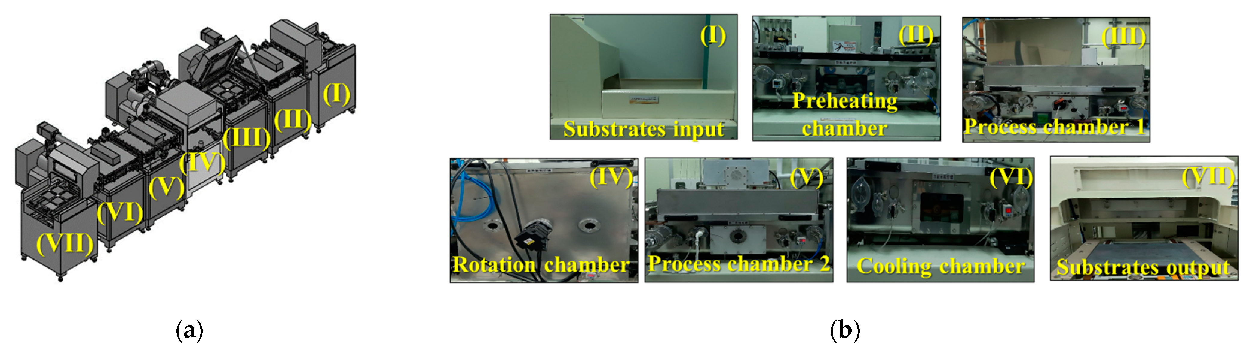
2. Materials and Methods

Figure 1 displays the schematic of the passivation layer of nc-Si:H deposited on a 300 μm thick n-type polished float zone (FZ) wafer with resistivity of 5 Ω-cm. The 20 nm intrinsic nc-Si:H was deposited on the top and bottom of the c-Si substrate. In applying the symmetric structure, the passivation layer of nc-Si:H played a crucial role in reducing the surface recombination and defects at an interface between the highly doped crystalline thin film and the c-Si substrate [40]. The 40.68 MHz VHFPECVD process is illustrated in Figure 2.
Figure 3 displays the deposition of nc-Si:H on the n-type crystalline silicon substrates. Here, nc-Si:H was deposited through VHFPECVD at a ratio (H2/SiH4) of 23%; a total flow rate of 50 sccm; a substrate temperature of 150 °C; chamber pressures of 0.2, 0.4, 0.6, and 0.8 Torr; and a power density of 40 mW/cm2. The electrode area was 1681 cm2, and the electrode–substrate distance was 15 mm. The c-Si substrate was cleaned first using a standard Radio Corporation of America (RCA) cleaning technique [41]. Immediately before the nc-Si:H deposition, the native oxide was removed from the c-Si substrate by dipping the c-Si substrate into 5% hydrofluoric acid (HF) for 30 s. VHFPECVD was performed to deposit the nc-Si:H at a c-Si substrate temperature of 150 °C. The top nc-Si:H was 20 nm thick. The deposition completed nc-Si:H/c-Si upside down through the rotation chamber and repeated the deposition step. The thickness of the bottom nc-Si:H was 20 nm. MWA was used in the last step.
The properties of the deposited symmetric structures are summarized in Table 1. Figure 4a displays the thermal image of the samples and various MWA times, as well as corresponding operating temperatures. The use of MWA on the prepared thin films was performed in a 2.45 GHz microwave annealing system with RF power of 100–1320 W. The in situ temperature of each sample was monitored by a Fluke Ti10 infrared camera. A Renishaw Invia Raman microscope was used to study the crystalline volume fraction of the film (with a 514 nm laser). To avoid the influence of signal from the c-Si substrate, the 20 nm nc-Si:H thin film/glass substrate was used to measure the Raman spectrum. The microwave annealing system (PYRO 260 Microwave System, purchased from Milestone Inc. in Milan, Italy) was used for sample microwave annealing. The FTIR spectra were recorded using an Agilent 660 spectrometer. The FTIR measurement signal was weak due to the nc-Si:H’s thickness, so we increased the thickness to about 1 μm and deposited it on the glass. Thus, we were able to observe the difference in FTIR spectra after microwave annealing. Wavenumbers were scanned from 670 to 4000 cm−1 at a scan rate of 0.4 cm s−1.
The variations of surface morphology and root mean square (RMS) roughness as a function of before and after MWA were evaluated using an atomic force microscope (AFM, NT-MDT Solver P47 system). The wavelength-dependent ellipsometric parameters, refractive index, and extinction coefficient (n, k) were measured using spectroscopic ellipsometry (M2000-DI, J. A. Woollam Co., Lincoln, NE, USA) at three incident angles of 55°, 65°, and 75°, and a wavelength ranging from 350 to 1100 nm. The carrier lifetime for samples without contacts was measured with a Sinton WCT-120 lifetime tester.

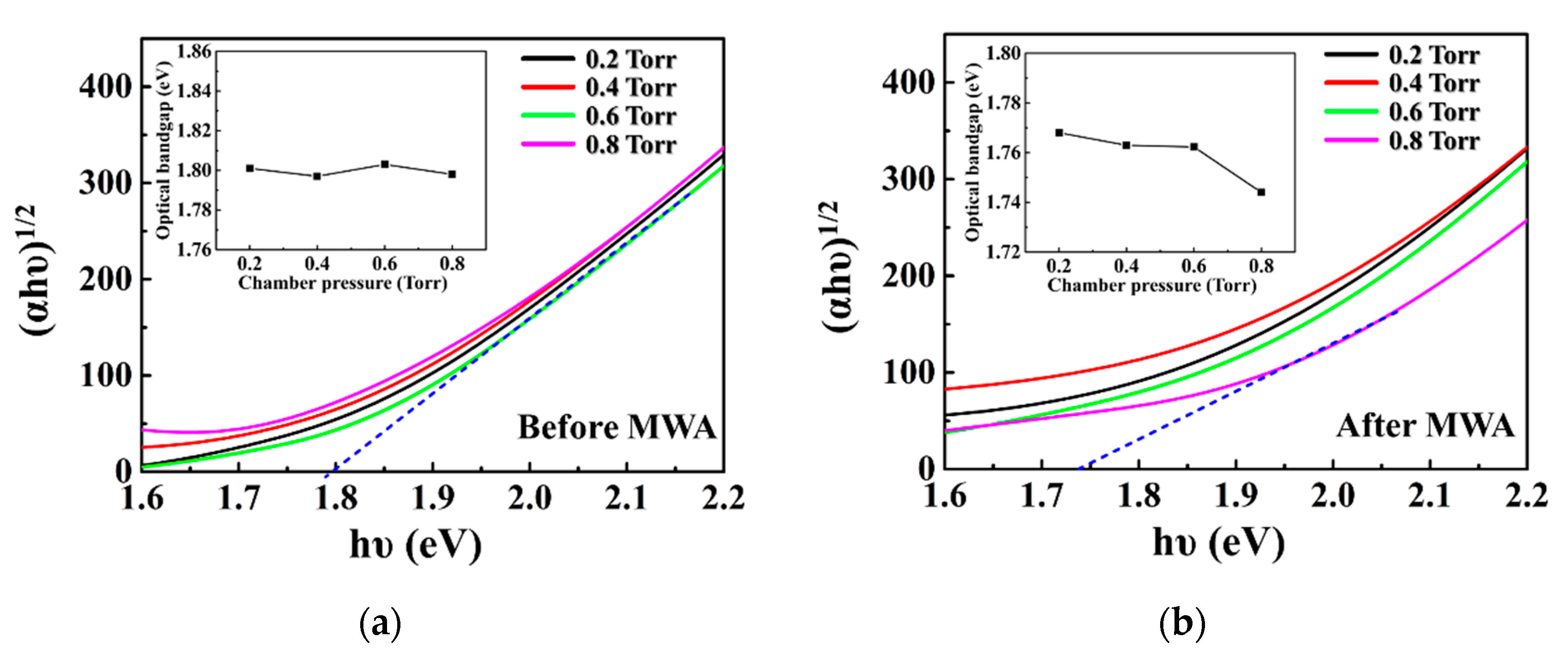
3. Results and Discussion

In the microwave annealing process, the collisions between the electrons (or holes) and silicon lattices induced resistivity heating inside the deposited Si thin films, which caused the realignment of the Si atoms [36]. MWA was rapid (9 °C/min), and uniformly (±6.8 °C/cm2) heated the thin films. This study provided a practical annealing approach to achieve a high-quality thin film of nc-Si:H. Figure 4b displays MWA at various powers and operating temperatures. The MWA temperature increased with an increase in microwave power. Low-temperature annealing is beneficial for the interface passivation quality, and an annealing temperature of 180 °C can yield interface recombination activity [42].
Figure 5 displays the deposition rate of the thin film as a function of chamber pressures of 0.2 to 0.8 Torr. The deposition rate was proportional to the chamber pressure in the VHFPECVD process. By increasing the chamber pressures from 0.2 to 0.8 Torr, the surface mobility of the VHFPECVD plasma increased [43], which increased the possibility of collisions of H2/SiH4 molecules. The high chamber pressures resulted in the fast growth rate of the nc-Si:H in the VHFPECVD process because the ions’ and radicals’ molecule reactions in the VHFPECVD became frequent and achieved high energy, increasing the deposition rate of the thin films [44]. However, promoting gas-phase particle formation instead resulted in dust-particle generation at the substrate of the deposition chamber at a higher deposition pressure.
Figure 6 displays a comparison of deconvoluted Raman spectra of the crystalline volume fraction of the deposited nc-Si:H on the glass substrate before and after MWA. The crystalline volume fraction (Xc) can be found by [45]:
Xc = Ic/(Ic + yIa)
where Ic, Ia, and y are the amorphous integrated intensities of the crystallite volume fraction, and ∑c/∑a is the ratio of the Raman diffusion cross-section for c-Si over that of thin film [46] The scattering cross-section ratio was estimated to be 0.88, according to the results presented by R. Tsu [47]. When the chamber pressures of VHFPECVD increased from 0.2 to 0.8 Torr, the crystalline volume fraction of the nc-Si:H increased from 13.5 to 21.9%. Many hydrogen-vacuum regions were generated due to the chamber pressure increase, causing grain growth [48]. When the pressure was too low, the number of silicon atoms was too few to enable them as nucleation centers. At the same time, the number of silicon atoms at a higher pressure was too high, which produced too many nucleation centers, which was not favorable to an increase in the growth of grains in the amorphous phase [45]. Chaochao et al. [36] found that the key factors for microwave absorption are the high density of dipoles from the thin film (high density of defects). The high-density defects come from an amorphous phase in the mixed-phase thin film. After MWA, the crystalline volume fraction of the nc-Si:H (0.8 Torr) increased considerably, from 21.9 to 29.6%, and exhibited increased nano-crystalline structures inside the thin film [4,49].
Figure 7 displays the Fourier transform infrared spectroscopy (FTIR) with 950 to 2300 cm−1 variation before and after microwave annealing at a chamber pressure of 0.8 Torr. The spectra also exhibit peaks, with one centered at ~1050 cm−1. The Si-H2 intensity reduction after using MWA showed that the nc-Si:H hydrogen content of the nc-Si:H had decreased [50], and the nano-crystalline of the mixed-phase had increased [51]. Among these, there were more Si-H and Si-H2 in the nc-Si:H film after deposition, and the characteristics (high density of defects) of microwave annealing helped to achieve the recrystallization effect due to the rapid release of surface hydrogen. The reduced concentration of O impurity (O-Si-O) in the nc-Si:H seemed to be related to decreased defect density [52]. Therefore, the recrystallization and reduction in nc-Si:H defect density could be achieved simply and quickly through MWA.
Figure 8 displays the atomic force microscopy images of the nc-Si:H under a chamber pressure of 0.8 Torr before and after MWA. The crystalline volume fraction of the nc-Si:H was 29.6%, and for the root mean square (RMS), there was little difference after MWA. However, a major problem with this kind of crystallinity is only a nanometer-level change (≈10%), so the process did not affect changes in the film morphology.
The refractive index and extinction coefficient (n, k) of the nc-Si:H were measured through spectroscopic ellipsometry. The absorption coefficient (α) of the nc-Si:H was obtained using the following formula [53,54]:
α = 4πk/λ
where k indicates the extinction coefficient and λ is the wavelength of visible light at 300 to 1100 nm. The optical bandgap (Eg) and absorption coefficient (α) are given by [53,54]:
(αhυ)1/2 = B(hυ − Eg)
where B is the optical density of state, hυ is the energy of light, and Eg is the optical bandgap. Figure 9 displays the optical bandgap of the deposited nc-Si:H before and after MWA under different chamber pressures in the VHFPECVD process.
In this study, the deposited thin films had an optical bandgap exceeding 1.8 eV, confirming that they were mixed-phase silicon thin films. In some studies [55,56], the increase in the chamber pressure led to a reduction in the optical bandgap, suggesting an increment in the defect density. Consistent with previous findings, the film defect density was helpful for microwave absorption. The dielectric polarization and ohmic conduction losses generated during MWA changed the nanoclusters in the mixed-phase silicon thin films to produce uniform bonding reactions [36]. The nanoclusters had non-fully crystallized grain growth to the coalescence stage. With microwave annealing, the increase in nanoclusters led to a reduction in the optical bandgap in all cases. Many studies have shown that the influence of the mixed phase on the optical bandgap is related to the size ratio and nanoclusters of the amorphous phase to the nanocrystal phase [57,58,59]. Therefore, the quality of the film can be improved when the mixed-phase film, through microwave annealing, causes the amorphous phase to begin to produce the nanocrystal phase. Notably, based on these studies, we believe the use of nc-Si:H mixed-phase thin films in symmetric structures can be discussed in more depth.
Figure 10 displays the carrier lifetime of the thin film (symmetric structures) after microwave annealing at 0.2 to 0.8 Torr chamber pressures in the VHFPECVD process. The microwave annealing treatment on the deposited symmetric structures resulted in a high carrier lifetime of 2942.36 µs and a crystalline volume fraction of 29.6%. In addition, the crystalline surface effectively reduced defect density [60]; therefore, it can be seen that the best carrier lifetime was achieved at a chamber pressure of 0.8 Torr and after annealing. It is known that the recrystallization effect will occur after microwave annealing. Notably, although the recrystallization effect will increase crystallinity, a significant problem of crystallinity is nanometer-level change (≈10%). Studies of the size ratio and distribution of the amorphous phase to the nanocrystals phase showed the importance of the mixed-phase thin film. This result suggested that when the mixed-phase thin film was microwave-annealed, the optical bandgap would be from 1.8 to 1.76 eV when the nanophase was grown, resulting in only a nanometer-level change. Thus, the method gave a more realistic estimate of the actual merit of the nc-Si:H thin films for symmetric structures. Table 2 compares the current and previous study results.

4. Conclusions

In this paper, an approach to depositing nc-Si:H using VHFPECVD under different chamber pressures and treating by microwave annealing to achieve the high-quality nc-Si:H was proposed. The relationships between the chamber pressures of the VHFPECVD and MWA on the nc-Si:H depositions were investigated. The chamber pressures (0.2, 0.4, 0.6, and 0.8 Torr) of the VHFPECVD process were critical factors in controlling the nc-Si:H carrier lifetime. Microwave annealing at a power of 440 W, a temperature of 180 °C, and a duration of 20 min were used to further improve the deposited nc-Si:H. The deposited nc-Si:H with a crystalline volume fraction of 29.6%, an optical bandgap of 1.744 eV, and a carrier lifetime of 2942.36 μs was well achieved. This study provided an effective method to accomplish the passivation layer of nano-crystalline silicon mixed-phase thin film in the applications of symmetric structures.

Author Contributions

Conceptualization, J.-H.L. and H.-W.W.; methodology, J.-H.L. and W.-C.T.; formal analysis, J.-H.L.; investigation, J.-H.L., W.-C.T. and C.-Y.H.; resources, W.-C.T. and C.-Y.H.; writing—original draft preparation, J.-H.L. and H.-W.W.; writing—review and editing, J.-H.L., H.-W.W. and S.-K.L.; visualization, J.-H.L., H.-W.W. and S.-K.L.; supervision, H.-W.W. All authors have read and agreed to the published version of the manuscript.

Funding

This study was supported by Taiwan’s Ministry of Science and Technology (MOST) under contract number MOST 107-2622-E-168-002-CC3 and MOST 107-2221-E-168-012-MY2.

Data Availability Statement

Experimental data is available upon request.

Acknowledgments

The authors would like to acknowledge the help they received from the Metal Industries Research & Development Centre (MIRDC) in Taiwan.

Conflicts of Interest

The authors declare no conflict of interest.

References

  1. Rahman, M.Z.; Khan, S.I. Advances in Surface Passivation of C-Si Solar Cells. Mater. Renew. Sustain. Energy. 2012, 1, 1. [Google Scholar] [CrossRef]
  2. Aberle, A.G. Surface Passivation of Crystalline Silicon Solar Cells: A Review. Prog. Photovolt. Res. Appl. 2000, 8, 473–487. [Google Scholar] [CrossRef]
  3. Anna Selvan, J.A.; Delahoy, A.E.; Guo, S.; Li, Y.-M. A New Light Trapping TCO for Nc-Si:H Solar Cells. Sol. Energy Mater. Sol. Cells. 2006, 90, 3371–3376. [Google Scholar] [CrossRef]
  4. Shim, J.-H.; Im, S.; Cho, N.-H. Nanostructural Features of Nc-Si:H Thin Films Prepared by PECVD. Appl. Surf. Sci. 2004, 234, 268–273. [Google Scholar] [CrossRef]
  5. Wen, C.; Xu, H.; Liu, H.; Li, Z.; Shen, W. Passivation of Nanocrystalline Silicon Photovoltaic Materials Employing a Negative Substrate Bias. Nanotechnology 2013, 24, 455602. [Google Scholar] [CrossRef] [PubMed]
  6. Zhang, Q.; Zhu, M.; Liu, F.; Zhou, Y. The Optimization of Interfacial Properties of Nc-Si:H/c-Si Solar Cells in Hot-Wire Chemical Vapor Deposition Process. J. Mater. Sci. Mater. Electron. 2007, 18, 33–36. [Google Scholar] [CrossRef]
  7. Sharma, M.; Panigrahi, J.; Komarala, V.K. Nanocrystalline Silicon Thin Film Growth and Application for Silicon Heterojunction Solar Cells: A Short Review. Nanoscale Adv. 2021, 3, 3373–3383. [Google Scholar] [CrossRef]
  8. Zhang, R.; Chen, X.Y.; Zhang, K.; Shen, W.Z. Photocurrent Response of Hydrogenated Nanocrystalline Silicon Thin Films. J. Appl. Phys. 2006, 100, 104310. [Google Scholar] [CrossRef]
  9. Chen, X.Y.; Shen, W.Z.; He, Y.L. Enhancement of Electron Mobility in Nanocrystalline Silicon∕crystalline Silicon Heterostructures. J. Appl. Phys. 2005, 97, 024305. [Google Scholar] [CrossRef]
  10. Keppner, H.; Meier, J.; Torres, P.; Fischer, D.; Shah, A. Microcrystalline Silicon and Micromorph Tandem Solar Cells. Appl. Phys. 1999, A 69, 169–177. [Google Scholar] [CrossRef] [Green Version]
  11. Edelberg, E.; Bergh, S.; Naone, R.; Hall, M.; Aydil, E.S. Visible Luminescence from Nanocrystalline Silicon Films Produced by Plasma Enhanced Chemical Vapor Deposition. Appl. Phys. Lett. 1996, 68, 1415–1417. [Google Scholar] [CrossRef]
  12. Zaknoon, B.; Bahir, G.; Saguy, C.; Edrei, R.; Hoffman, A.; Rao, R.A.; Muralidhar, R.; Chang, K.-M. Study of Single Silicon Quantum Dots’ Band Gap and Single-Electron Charging Energies by Room Temperature Scanning Tunneling Microscopy. Nano Lett. 2008, 8, 1689–1694. [Google Scholar] [CrossRef] [PubMed]
  13. Gonçalves, C.; Charvet, S.; Zeinert, A.; Clin, M.; Zellama, K. Nanocrystalline Silicon Thin Films Prepared by Radiofrequency Magnetron Sputtering. Thin Solid Films 2002, 403–404, 91–96. [Google Scholar] [CrossRef]
  14. Fonrodona, M.; Soler, D.; Escarré, J.; Villar, F.; Bertomeu, J.; Andreu, J.; Saboundji, A.; Coulon, N.; Mohammed-Brahim, T. Low Temperature Amorphous and Nanocrystalline Silicon Thin Film Transistors Deposited by Hot-Wire CVD on Glass Substrate. Thin Solid Films 2006, 501, 303–306. [Google Scholar] [CrossRef] [Green Version]
  15. Takatsuka, H.; Noda, M.; Yonekura, Y.; Takeuchi, Y.; Yamauchi, Y. Development of High Efficiency Large Area Silicon Thin Film Modules Using VHF-PECVD. Sol. Energy 2004, 77, 951–960. [Google Scholar] [CrossRef]
  16. Dutta, J.; Kroll, U.; Chabloz, P.; Shah, A.; Howling, A.A.; Dorier, J.-L.; Hollenstein, C. Dependence of Intrinsic Stress in Hydrogenated Amorphous Silicon on Excitation Frequency in a Plasma-enhanced Chemical Vapor Deposition Process. J. Appl. Phys. 1992, 72, 3220–3222. [Google Scholar] [CrossRef] [Green Version]
  17. Surendra, M.; Graves, D.B. Capacitively Coupled Glow Discharges at Frequencies above 13.56 MHz. Appl. Phys. Lett. 1991, 59, 2091–2093. [Google Scholar] [CrossRef]
  18. Kitajima, T.; Takeo, Y.; Nakano, N.; Makabe, T. Effects of Frequency on the Two-Dimensional Structure of Capacitively Coupled Plasma in Ar. J. Appl. Phys. 1998, 84, 5928–5936. [Google Scholar] [CrossRef]
  19. Takagi, T.; Takechi, K.; Nakagawa, Y.; Watabe, Y.; Nishida, S. High Rate Deposition of A-Si:H and a-SiNx:H by VHF PECVD. Vacuum 1998, 51, 751–755. [Google Scholar] [CrossRef]
  20. Curtins, H.; Wyrsch, N.; Favre, M.; Shah, A.V. Influence of Plasma Excitation Frequency Fora-Si:H Thin Film Deposition. Plasma Chem. Plasma Process. 1987, 7, 267–273. [Google Scholar] [CrossRef]
  21. Batey, J.; Tierney, E. Low-temperature Deposition of High-quality Silicon Dioxide by Plasma-enhanced Chemical Vapor Deposition. J. Appl. Phys. 1986, 60, 3136–3145. [Google Scholar] [CrossRef]
  22. Matsui, T.; Kondo, M.; Matsuda, A. Origin of the Improved Performance of High-Deposition-Rate Microcrystalline Silicon Solar Cells by High-Pressure Glow Discharge. Jpn. J. Appl. Phys. 2003, 42, L901. [Google Scholar] [CrossRef]
  23. Gordijn, A.; Vanecek, M.; Goedheer, W.J.; Rath, J.K.; Schropp, R.E.I. Influence of Pressure and Plasma Potential on High Growth Rate Microcrystalline Silicon Grown by Very High Frequency Plasma Enhanced Chemical Vapour Deposition. Jpn. J. Appl. Phys. 2006, 45, 6166. [Google Scholar] [CrossRef]
  24. Sobajima, Y.; Nishino, M.; Fukumori, T.; Kurihara, M.; Higuchi, T.; Nakano, S.; Toyama, T.; Okamoto, H. Solar Cell of 6.3% Efficiency Employing High Deposition Rate (8 nm/s) Microcrystalline Silicon Photovoltaic Layer. Sol. Energy Mater. Sol. Cells 2009, 93, 980–983. [Google Scholar] [CrossRef]
  25. Klein, S.; Repmann, T.; Brammer, T. Microcrystalline Silicon Films and Solar Cells Deposited by PECVD and HWCVD. Sol. Energy 2004, 77, 893–908. [Google Scholar] [CrossRef]
  26. Yang, H.J.; Ji, K.; Choi, J.; Lee, H.M. Annealing Effect on Surface Passivation of A-Si:H/c-Si Interface in Terms of Crystalline Volume Fraction. Curr. Appl. Phys. 2010, 10, S375–S378. [Google Scholar] [CrossRef]
  27. Ai, Y.; Yuan, H.-C.; Page, M.; Nemeth, W.; Roybal, L.; Gedvilas, L.; Wang, Q. Process Optimization for High Efficiency Heterojunction C-Si Solar Cells Fabrication Using Hot-Wire Chemical Vapor Deposition. In Proceedings of the 2012 38th IEEE Photovoltaic Specialists Conference, Austin, TX, USA, 3–8 June 2012; pp. 988–991. [Google Scholar]
  28. De Wolf, S.; Demaurex, B.; Descoeudres, A.; Ballif, C. Very Fast Light-Induced Degradation of $a$-Si:H/$c$-Si(100) Interfaces. Phys. Rev. B 2011, 83, 233301. [Google Scholar] [CrossRef] [Green Version]
  29. Luo, Y.; Sui, X.; He, Y.; Huang, H.; Zhou, N.; Zhou, L. The Influence of Annealing Temperature upon the Structure of A-Si:H/c-Si Thin Films. J. Non-Cryst. Solids 2017, 471, 379–383. [Google Scholar] [CrossRef]
  30. Stöhr, M.; Aprojanz, J.; Brendel, R.; Dullweber, T. Firing-Stable PECVD SiOxNy/n-Poly-Si Surface Passivation for Silicon Solar Cells. ACS Appl. Energy Mater. 2021, 4, 4646–4653. [Google Scholar] [CrossRef]
  31. Schulze, T.F.; Beushausen, H.N.; Hansmann, T.; Korte, L.; Rech, B. Accelerated Interface Defect Removal in Amorphous/Crystalline Silicon Heterostructures Using Pulsed Annealing and Microwave Heating. Appl. Phys. Lett. 2009, 95, 182108. [Google Scholar] [CrossRef]
  32. Lu, Y.-L.; Lee, Y.-J.; Chao, T.-S. Simultaneous Activation and Crystallization by Low-Temperature Microwave Annealing for Improved Quality of Amorphous Silicon Thin-Film Transistors. ECS Solid State Lett. 2012, 1, P1. [Google Scholar] [CrossRef]
  33. Lee, Y.-J.; Cho, T.-C.; Chuang, S.-S.; Hsueh, F.-K.; Lu, Y.-L.; Sung, P.-J.; Chen, H.-C.; Current, M.I.; Tseng, T.-Y.; Chao, T.-S.; et al. Low-Temperature Microwave Annealing Processes for Future IC Fabrication—A Review. IEEE Trans. Electron Devices 2014, 61, 651–665. [Google Scholar] [CrossRef]
  34. Hu, H.-H.; Huang, H.-P. High-Frequency Performance of Trigate Poly-Si Thin-Film Transistors by Microwave Annealing. IEEE Electron Device Lett. 2015, 36, 345–347. [Google Scholar] [CrossRef]
  35. Shih, T.-L.; Su, Y.-H.; Kuo, T.-C.; Lee, W.-H.; Current, M.I. Effect of Microwave Annealing on Electrical Characteristics of TiN/Al/TiN/HfO2/Si MOS Capacitors. Appl. Phys. Lett. 2017, 111, 012101. [Google Scholar] [CrossRef]
  36. Fu, C.; Wang, Y.; Xu, P.; Yue, L.; Sun, F.; Zhang, D.W.; Zhang, S.-L.; Luo, J.; Zhao, C.; Wu, D. Understanding the Microwave Annealing of Silicon. AIP Adv. 2017, 7, 035214. [Google Scholar] [CrossRef] [Green Version]
  37. Lihui, G.; Rongming, L. Studies on the Formation of Microcrystalline Silicon with PECVD under Low and High Working Pressure. Thin Solid Films 2000, 376, 249–254. [Google Scholar] [CrossRef]
  38. Wang, Y.; Liu, H.; Shen, W. A Convenient and Effective Method to Deposit Low-Defect-Density Nc-Si:H Thin Film by PECVD. Nanoscale Res. Lett. 2018, 13, 234. [Google Scholar] [CrossRef]
  39. Suzuki, S.; Kondo, M.; Matsuda, A. Growth of Device Grade Μc-Si Film at over 50Å/s Using PECVD. Sol. Energy Mater. Sol. Cells 2002, 74, 489–495. [Google Scholar] [CrossRef]
  40. Wei, C.-Y.; Lin, C.-H.; Hsiao, H.-T.; Yang, P.-C.; Wang, C.-M.; Pan, Y.-C. Efficiency Improvement of HIT Solar Cells on P-Type Si Wafers. Materials 2013, 6, 5440–5446. [Google Scholar] [CrossRef] [Green Version]
  41. Liang, X.; Sperling, B.A.; Calizo, I.; Cheng, G.; Hacker, C.A.; Zhang, Q.; Obeng, Y.; Yan, K.; Peng, H.; Li, Q.; et al. Toward Clean and Crackless Transfer of Graphene. ACS Nano 2011, 5, 9144–9153. [Google Scholar] [CrossRef]
  42. De Wolf, S.; Olibet, S.; Ballif, C. Stretched-Exponential a-Si:H/c-Si Interface Recombination Decay. Appl. Phys. Lett. 2008, 93, 032101. [Google Scholar] [CrossRef]
  43. Andújar, J.L.; Bertran, E.; Canillas, A.; Roch, C.; Morenza, J.L. Influence of Pressure and Radio Frequency Power on Deposition Rate and Structural Properties of Hydrogenated Amorphous Silicon Thin Films Prepared by Plasma Deposition. J. Vac. Sci. Technol. A 1991, 9, 2216–2221. [Google Scholar] [CrossRef] [Green Version]
  44. Matsuda, A. Growth Mechanism of Microcrystalline Silicon Obtained from Reactive Plasmas. Thin Solid Films 1999, 337, 1–6. [Google Scholar] [CrossRef]
  45. Bustarret, E.; Hachicha, M.A.; Brunel, M. Experimental Determination of the Nanocrystalline Volume Fraction in Silicon Thin Films from Raman Spectroscopy. Appl. Phys. Lett. 1988, 52, 1675–1677. [Google Scholar] [CrossRef]
  46. Droz, C.; Vallat-Sauvain, E.; Bailat, J.; Feitknecht, L.; Meier, J.; Shah, A. Relationship between Raman Crystallinity and Open-Circuit Voltage in Microcrystalline Silicon Solar Cells. Sol. Energy Mater. Sol. Cells 2004, 81, 61–71. [Google Scholar] [CrossRef] [Green Version]
  47. Tsu, R.; Gonzalez-Hernandez, J.; Chao, S.S.; Lee, S.C.; Tanaka, K. Critical Volume Fraction of Crystallinity for Conductivity Percolation in Phosphorus-doped Si:F:H Alloys. Appl. Phys. Lett. 1982, 40, 534–535. [Google Scholar] [CrossRef]
  48. Amrani, R.; Pichot, F.; Podlecki, J.; Foucaran, A.; Chahed, L.; Cuminal, Y. Optical and Structural Proprieties of Nc-Si:H Prepared by Argon Diluted Silane PECVD. J. Non-Cryst. Solids 2012, 358, 1978–1982. [Google Scholar] [CrossRef]
  49. Funde, A.M.; Bakr, N.A.; Kamble, D.K.; Hawaldar, R.R.; Amalnerkar, D.P.; Jadkar, S.R. Influence of Hydrogen Dilution on Structural, Electrical and Optical Properties of Hydrogenated Nanocrystalline Silicon (Nc-Si:H) Thin Films Prepared by Plasma Enhanced Chemical Vapour Deposition (PE-CVD). Sol. Energy Mater. Sol. Cells 2008, 92, 1217–1223. [Google Scholar] [CrossRef]
  50. Kroll, U.; Meier, J.; Shah, A.; Mikhailov, S.; Weber, J. Hydrogen in Amorphous and Microcrystalline Silicon Films Prepared by Hydrogen Dilution. J. Appl. Phys. 1996, 80, 4971–4975. [Google Scholar] [CrossRef]
  51. Shim, J.-H.; Cho, N.-H. Structural and Chemical Features of Silicon Nanocrystallites in Nanocrystalline Hydrogenated Silicon Thin Films. Glass Phys. Chem. 2005, 31, 525–529. [Google Scholar] [CrossRef]
  52. Lucovsky, G.; Nemanich, R.J.; Knights, J.C. Structural Interpretation of the Vibrational Spectra of $a$-Si:H Alloys. Phys. Rev. B 1979, 19, 2064–2073. [Google Scholar] [CrossRef]
  53. Peng, C.H.; Chang, J.-F.; Desu, S.B. Optical Properties of PZT, PLZT, and PNZT Thin Films. MRS Online Proc. Libr. OPL 1991, 243. [Google Scholar] [CrossRef]
  54. Yang, S.; Mo, D.; Tang, X. Determination of the Optical Properties of Sol-Gel-Derived Pb(Zr x Ti (1 − x ) )O 3 Thin Films by Spectroscopic Ellipsometry. Ferroelectrics 2003, 287, 35–46. [Google Scholar] [CrossRef]
  55. Li, W.; Xia, D.; Wang, H.; Zhao, X. Hydrogenated Nanocrystalline Silicon Thin Film Prepared by RF-PECVD at High Pressure. J. Non-Cryst. Solids 2010, 356, 2552–2556. [Google Scholar] [CrossRef]
  56. Jadhavar, A.; Pawbake, A.; Waykar, R.; Jadkar, V.; Kulkarni, R.; Bhorde, A.; Rondiya, S.; Funde, A.; Patil, D.; Date, A.; et al. Growth of Hydrogenated Nano-Crystalline Silicon (Nc-Si:H) Films by Plasma Enhanced Chemical Vapor Deposition (PE-CVD). Energy Procedia 2017, 110, 45–52. [Google Scholar] [CrossRef]
  57. Wang, Y.H.; Lin, J.; Huan, C.H.A. Structural and Optical Properties of A-Si:H/Nc-Si:H Thin Films Grown from Ar–H2–SiH4 Mixture by Plasma-Enhanced Chemical Vapor Deposition. Mater. Sci. Eng. B 2003, 104, 80–87. [Google Scholar] [CrossRef]
  58. Canham, L.T. Silicon Quantum Wire Array Fabrication by Electrochemical and Chemical Dissolution of Wafers. Appl. Phys. Lett. 1990, 57, 1046–1048. [Google Scholar] [CrossRef]
  59. Juneja, S.; Sudhakar, S.; Gope, J.; Kumar, S. Mixed Phase Silicon Thin Films Grown at High Rate Using 60MHz Assisted VHF-PECVD Technique. Mater. Sci. Semicond. Process. 2015, 40, 11–19. [Google Scholar] [CrossRef]
  60. Schulze, T.F.; Beushausen, H.N.; Leendertz, C.; Dobrich, A.; Rech, B.; Korte, L. Interplay of Amorphous Silicon Disorder and Hydrogen Content with Interface Defects in Amorphous/Crystalline Silicon Heterojunctions. Appl. Phys. Lett. 2010, 96, 252102. [Google Scholar] [CrossRef]
  61. Guo, C.-L.; Wang, L.; Zhang, Y.-R.; Zhou, H.-F.; Liang, F.; Yang, Z.-H.; Yang, D.-R. High-Pressure Water-Vapor Annealing for Enhancement of a-Si:H Film Passivation of Silicon Surface. Chin. Phys. Lett. 2014, 31, 108501. [Google Scholar] [CrossRef]
  62. Chu, Y.-H.; Lee, C.-C.; Chang, T.-H.; Hsieh, Y.-L.; Liu, S.-M.; Chang, J.-Y.; Li, T.T.; Chen, I.-C. Investigation of A-Si:H Films as Passivation Layer in Heterojunction Interface at Low Temperature. ECS Trans. 2014, 60, 1245. [Google Scholar] [CrossRef]
  63. Ruan, T.; Qu, M.; Wang, J.; He, Y.; Xu, X.; Yu, C.; Zhang, Y.; Yan, H. Effect of Deposition Temperature of A-Si:H Layer on the Performance of Silicon Heterojunction Solar Cell. J. Mater. Sci. Mater. Electron. 2019, 30, 13330–13335. [Google Scholar] [CrossRef]
  64. Gotoh, K.; Wilde, M.; Kato, S.; Ogura, S.; Kurokawa, Y.; Fukutani, K.; Usami, N. Hydrogen Concentration at A-Si:H/c-Si Heterointerfaces—The Impact of Deposition Temperature on Passivation Performance. AIP Adv. 2019, 9, 075115. [Google Scholar] [CrossRef] [Green Version]
  65. El Whibi, S.; Derbali, L.; Tristant, P.; Jaoul, C.; Colas, M.; Mayet, R.; Cornette, J.; Ezzaouia, H. Optimized Nc-Si:H Thin Films with Enhanced Optoelectronic Properties Prepared by Micro-Waves PECVD Used as an Effective Silicon Surface Passivation Layer. J. Mater. Sci. Mater. Electron. 2019, 30, 2351–2359. [Google Scholar] [CrossRef]
  66. Lu, C.-C.; Hsieh, Y.-L.; Wu, P.-S.; Lee, C.-C.; Chu, Y.-H.; Chang, J.-Y.; Chen, I.-C.; Li, T.T. Advances N-Type Nc-Si:H Layers Depositing on Passivation Layer Applied to the Back Surface Field Prepared by RF-PECVD. In Proceedings of the 2015 China Semiconductor Technology International Conference, Shanghai, China, 15–16 March 2015; pp. 1–3. [Google Scholar]
  67. De Vrijer, T.; Smets, A.H.M. Advanced Textured Monocrystalline Silicon Substrates with High Optical Scattering Yields and Low Electrical Recombination Losses for Supporting Crack-Free Nano- to Poly-Crystalline Film Growth. Energy Sci. Eng. 2021, 9, 1080–1089. [Google Scholar] [CrossRef]
Figure 1. Schematic structure of the passivation layer of nc-Si:H deposited on an n-type crystalline silicon substrate.
Electronics 10 02199 g001
Figure 2. The use of the in-line 40.68 MHz VHFPECVD in this study: (a) equipment diagram; (b) entity diagram. (I) The substrates input; (II) the preheating chamber; (III) process chamber 1 for depositing the nc-Si:H; (IV) the rotation chamber for depositing the thin film on the back of the substrate; (V) process chamber 2 for depositing the nc-Si:H on the back of substrates; (VI) the cooling chamber; and (VII) the substrate output.
Electronics 10 02199 g002
Figure 3. Fabrication process flow of the deposition of nc-Si:H on an n-type crystalline silicon substrate.
Electronics 10 02199 g003
Figure 4. (a) Thermal image and (b) surface temperature of the thin film through microwave annealing.
Electronics 10 02199 g004
Figure 5. The deposition rate of the thin film as a function of chamber pressures of 0.2 to 0.8 Torr, with a power density of 40 mW/cm2, a substrate temperature of 150 °C, and a H2/SiH4 flow of 50 sccm for all cases.
Electronics 10 02199 g005
Figure 6. (a) The crystalline volume fraction of the deposited nc-Si:H as a function of chamber pressures before and after treating with MWA. (b) Deconvoluted Raman spectra after treating with MWA of nc-Si:H deposited on the glass substrate at a chamber pressure of 0.8 Torr. In all cases, the power density was 40 mW/cm2, the substrate temperature was 150 °C, and the H2/SiH4 flow was 50 sccm.
Electronics 10 02199 g006
Figure 7. Fourier transform infrared spectroscopy (FTIR) of the thin film at a 0.8 Torr chamber pressure before and after using microwave annealing.
Electronics 10 02199 g007
Figure 8. AFM images of the thin film under 0.8 Torr chamber pressure (a) before microwave annealing and (b) after microwave annealing. A microwave annealing power of 440 W, an annealing temperature of 180 °C, and an MWA time of 20 min were used in all cases.
Electronics 10 02199 g008
Figure 9. Optical bandgap of the thin film (a) before using microwave annealing and (b) after microwave annealing at different chamber pressures. in all cases, the MWA power was 440 W, the annealing temperature was 180 °C, and the MWA time was 20 min.
Electronics 10 02199 g009
Figure 10. Carrier lifetime of the thin film (symmetric structures) after microwave annealing. In all cases, the c-Si substrate size was 2.5 cm2, the MWA power was 440 W, the annealing temperature was 180 °C, and the MWA time was 20 min.
Electronics 10 02199 g010
Table 1. Properties of the deposited nc-Si:H mixed-phase thin films. Note: MWA = microwave annealing.
Chamber
Pressure (Torr)
Power Density (mW/cm2)Substrate
Temperature (°C)
H2/SiH4 (sccm)MWA
Temperature (°C)
Carrier Lifetime (µs)
before
Passivation
without MWAafter MWA
0.240150501804.3225.43688.03
0.440150501804.0127.531140.95
0.640150501806.2911.831228.35
0.840150501805.08131.292942.36
Table 2. Comparison of carrier lifetime, annealing method, annealing temperatures, and annealing time performance between the previous research and the current study. Note: a-Si:H = amorphous silicon; c-Si = crystalline silicon; HWA = high-pressure water-vapor annealing; MWA = microwave annealing; x = not reported in the reference; PDA = post-deposition annealing; SHJ = silicon hetero junction; BSF = back surface field.
Ref.StructuresAnnealing MethodAnnealing
Temperatures (°C)
Annealing
Time (min)
Optical
Bandgap (eV)
Carrier Lifetime (µs)
[61]a-Si:H/c-Si/a-Si:HHWA21060x72
[62]a-Si:H/c-Si/a-Si:HAnnealing2702x883
[63]SHJ (a-Si:H)xxx1.811774
[64]a-Si:H/c-SiPDA20030x~2000
[65]nc-Si:H/c-Sixxxx1987
[66]BSF (nc-Si:H)xxx1.76~1500
[67]a-Si:H/c-Si/a-Si:HAnnealing18030x~1000
This worknc-Si:H/c-Si/nc-Si:HMWA180201.7442942.36
Publisher’s Note: MDPI stays neutral with regard to jurisdictional claims in published maps and institutional affiliations.

