
GaN-Based PCSS with High Breakdown Fields

Abstract
:1. Introduction
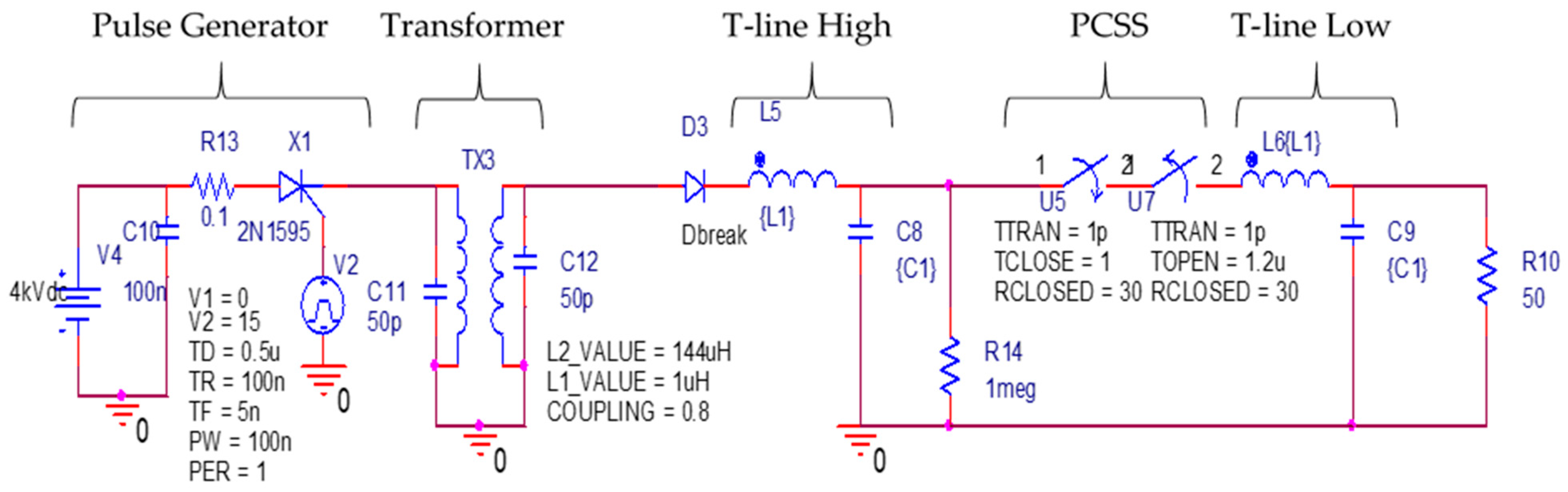
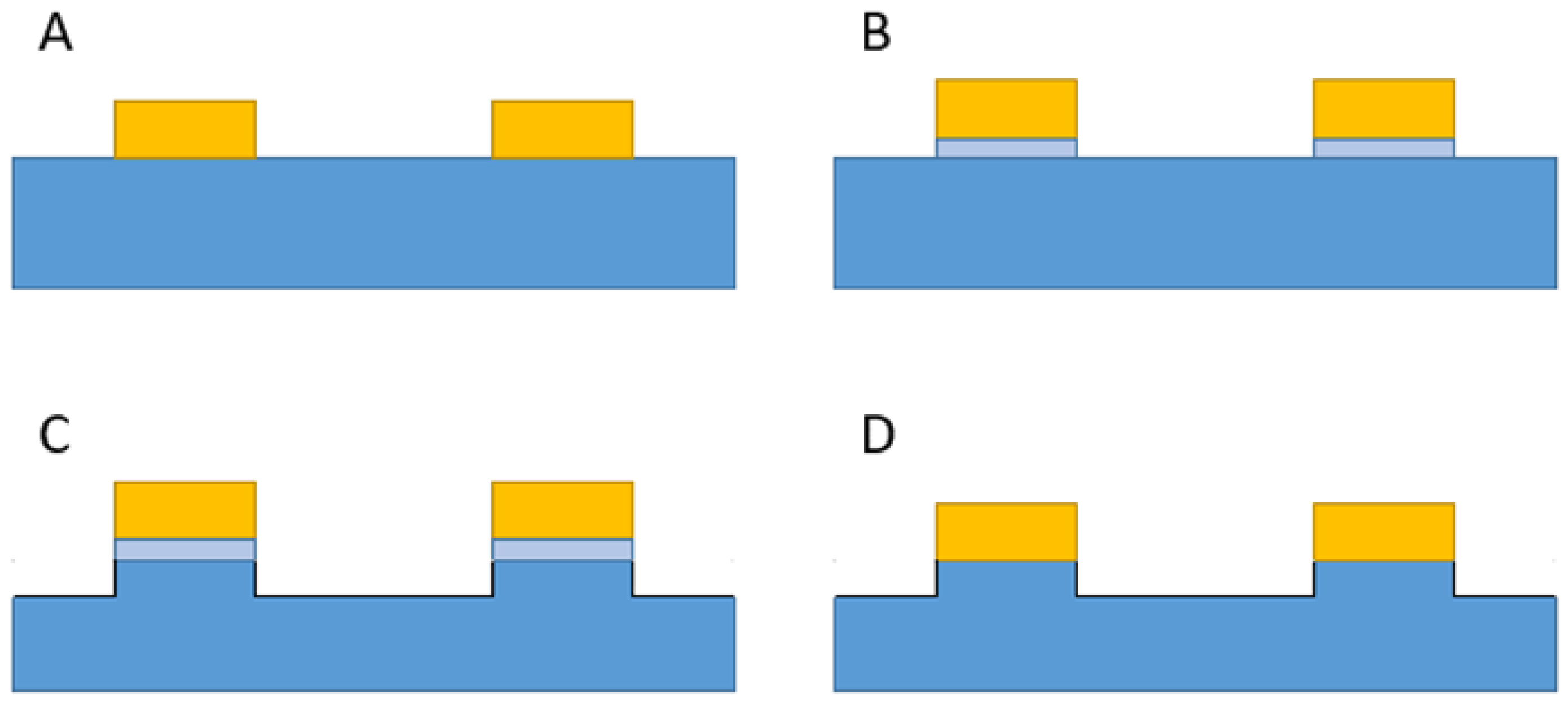
2. Processing
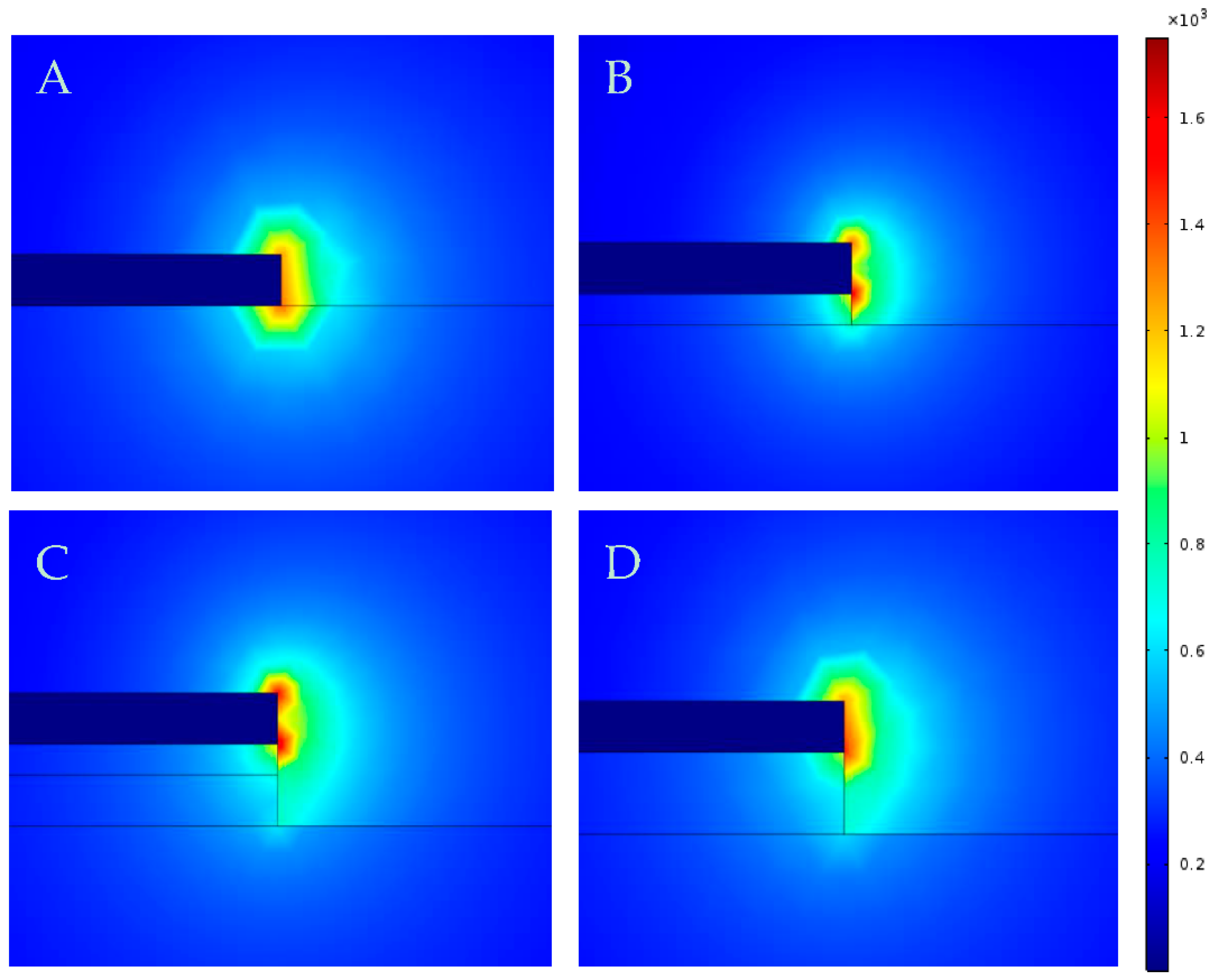
3. Design
4. Discussion
5. Conclusions
Author Contributions
Funding
Data Availability Statement
Conflicts of Interest
References
- Loubriel, G.M.; Zutavern, F.J.; Hjalmarson, H.P.; O’Malley, M.W. Closing photoconductive semiconductor switches. In Proceedings of the 7th Pulsed Power Conference, Monterey, CA, USA, 11–14 June 1989; pp. 365–367. [Google Scholar]
- Zutavern, F.J.; Loubruel, G.M.; O′Malley, M.W.; Shanwald, L.P.; Helgeson, W.D.; McLaughlin, D.L.; McKenzie, B.B. Photoconductive semiconductor switch experiments for pulsed power applications. IEEE Trans. Electron Devices 1990, 37, 2472–2477. [Google Scholar] [CrossRef]
- Rais-Zadeh, M.; Gokhale, V.J.; Ansari, A.; Faucher, M.; Théron, D.; Cordier, Y.; Buchaillot, L. Gallium Nitride as Electromechanical material. J. Microelectromech. Syst. 2014, 23, 1252–1271. [Google Scholar] [CrossRef]
- Iwinska, M.; Zajac, M.; Lucznik, B.; Fijalkowski, M.; Amilusik, M.; Sochacki, T.; Litwin-Staszewska, E.; Piotrzkowski, R.; Grzegory, I.; Bockowski, M. Iron and manganese as dopants used in the crystallization of highly resistive HVPE-GaN on native seeds. Jpn. J. Appl. Phys. 2019, 58, SC1047. [Google Scholar] [CrossRef]
- Mar, A.; Hirsch, E.; Zutavern, F.; Pickrell, G.; Delhotal, J.; Gallegos, R.; Bigman, V.; Struve, K.; Teague, J.; Lehr, J.; et al. High-Gain Persistent Nonlinear Conductivity in High-Voltage Gallium Nitride Photoconductive Switches. In Proceedings of the 2018 IEEE International Power Modulator and High Voltage Conference, Jackson, WY, USA, 3–7 June 2018. [Google Scholar]
- Gaddy, M.; Kuryatkov, V.; Meyers, V.; Mauch, D.; Dickens, J.; Neuber, A.; Nikishin, S. Structural, morphological, optical and electrical properties of bulk (0001) GaN:Fe wafers. MRS Adv. 2018, 3, 179–184. [Google Scholar] [CrossRef]
- Chowdhury, A.R.; Nikishin, S.; Dickens, J.; Neuber, A.; Joshi, R.P.; Ness, R. Numerical srudies into the parameter space conductive to “lock-on” in a GaN photoconductive switch for high power applications. IEEE Trans. Dielectr. Electr. Insul. 2019, 26, 469. [Google Scholar] [CrossRef]
- Meyers, V.; Mauch, D.; Kuryatkov, V.; Nikishin, S.; Dickens, J.; Neuber, A.; Ness, R. Toward the development of an efficient bulk semi-insulating GaN photoconductive switch. In Proceedings of the 2017 IEEE 21st International Conference on Pulsed Power, Brighton, UK, 18–22 June 2017. [Google Scholar]
- Fen, W.; Kuryatkov, V.; Nikishin, S.; Holtz, M. Selective area epitaxy of InGaN quantum well triangular microrings with a single type of sidewall facets. J. Cryst. Growth 2010, 312, 1717–1720. [Google Scholar]


| Sample Geometry | Gap Spacing | Applied Voltage | Average Field | Simulated Peak Field |
|---|---|---|---|---|
| Metal Contacts | 3 mm | 39 kV | ~130 kV/cm | ~2.1 MV/cm |
| Conductive GaN Layer | 3 mm | 45 kV | ~150 kV/cm | ~2.1 MV/cm |
| Conductive GaN Layer with Mesa | 3 mm | 52.5 kV | ~175 kV/cm | ~2.2 MV/cm |
| Metal Contacts | 600 µm | 12.2 kV | ~200 kV/cm | ~3.2 MV/cm |
| Mesa | 600 µm | 15.6 kV | ~260 kV/cm | ~2.9 MV/cm |
Publisher’s Note: MDPI stays neutral with regard to jurisdictional claims in published maps and institutional affiliations. |
© 2021 by the authors. Licensee MDPI, Basel, Switzerland. This article is an open access article distributed under the terms and conditions of the Creative Commons Attribution (CC BY) license (https://creativecommons.org/licenses/by/4.0/).
Share and Cite
Gaddy, M.; Kuryatkov, V.; Wilson, N.; Neuber, A.; Ness, R.; Nikishin, S. GaN-Based PCSS with High Breakdown Fields. Electronics 2021, 10, 1600. https://doi.org/10.3390/electronics10131600
Gaddy M, Kuryatkov V, Wilson N, Neuber A, Ness R, Nikishin S. GaN-Based PCSS with High Breakdown Fields. Electronics. 2021; 10(13):1600. https://doi.org/10.3390/electronics10131600
Chicago/Turabian StyleGaddy, Matthew, Vladimir Kuryatkov, Nicholas Wilson, Andreas Neuber, Richard Ness, and Sergey Nikishin. 2021. "GaN-Based PCSS with High Breakdown Fields" Electronics 10, no. 13: 1600. https://doi.org/10.3390/electronics10131600