1. Introduction
Meander structures are used in many microwave devices [
1,
2,
3]. The most common application areas for meander structures are antennas [
4], antenna arrays [
5], phase shifters [
6], filters [
7], and slow-wave structures. Meander structures are also used in resonator designs [
8], pulse-forming lines [
9], meandered superinductors [
10], and others. One of the main reasons for using meander structures is the ability to miniaturize a microwave device. Meander structures also have other specific advantages that are specific to the field of application.
For example, the task of antenna miniaturization was solved in [
11]. The authors presented a compact and broadband coplanar waveguide-fed meander-slot antenna. A size of 30 × 20 mm
2 was achieved using a modified meander slot, which was combined with a Y-shape monopole and trident-shaped feed strip. The antenna was designed for WiFi, WiMax, and 5G applications and could work in a 2.33–3.56 GHz frequency range. A 1.6 mm thick FR4 dielectric
εr = 4.4 and tanδ = 0.02 substrate was used for the design. The width of the meander conductor varied between 0.5 mm and 0.9 mm at different locations. The meander structure allowed for reducing the dimensions of the antenna and increasing the external slot current path length and, as a result, for shifting the first resonance frequency to lower frequencies. The maximum gain value of the proposed antenna was about 2 dBi around 3.4 GHz. The gain did not fall below 0.6 dBi over the entire bandwidth of interest. The dimensions of the microstrip patch IoT antenna were reduced using the s-shape meander line in [
12]. The overall dimensions of the antenna were 40 × 10 × 1.6 mm
3. The resonant frequency of the antenna was 2.4 GHz. FR4 dielectric was used for the substrate. The authors focused on the selection of construction parameters to obtain optimal antenna performance characteristics, such as antenna peak gain, efficiency, and higher fractional bandwidth. The chosen structure of the antenna also allowed for getting higher efficiency and gain in comparison with a conventional meander shape antenna. Miniaturization is also relevant in devices, which work in lower frequency ranges. A traditional monopole antenna for a 140 MHz central frequency is huge and inconvenient to use. A 46% reduction in size using a meander line monopole was presented in [
13]. Fifteen meander sections had an overall footprint of 293 × 64.5 mm
2. The width of a meander conductor was 2.9 mm. The gap between adjacent conductors was equal to 5.9 mm. FR4 was used for the substrate. The antenna was designed for specific low-frequency electromagnetic surveying systems. The bandwidth of the antenna was 13 MHz, the directivity was 1.68 dBi, and the radiation efficiency was 80.2%.
Meander structures are also popular in filter design. Meander lines as symmetrical shunts were used in a vialess compact metamaterial band pass filter in [
14]. The filter was designed on an FR4 epoxy glass substrate with a dielectric constant of 4.4, a loss tangent of 0.02, and a thickness of 1.6 mm. The length of the meander line influenced the operating frequency range of the filter and the group delay time, which varied from 0.5 ns to 0.75 ns within the passband from 1.93 GHz to 4.3 GHz. The length of the meander conductor was 9.6 mm, the width of the conductor was 0.4 mm, and the gap between adjacent conductors was also 0.4 mm. A measured insertion loss of 0.70 dB and a return loss higher than 25 dB with a 3 dB fractional bandwidth of 50.4% at a central frequency of 2.62 GHz were obtained. A microstrip line filter with band stop characteristics is presented in [
15]. The miniaturization was achieved with a meander structure. The authors showed that the increasing order of the filter improves the band rejection characteristics. A second-order meander filter with a 2.4 GHz central frequency was fabricated and verified. The size of the meander structure was 2 × 16.3 mm
2. The width of the meander conductor was 0.7 mm. FR4 was used for the substrate.
Another big group of devices, which include meander structures, are slow-wave structures. A novel configuration of a Ka-band slow-wave structure is presented in [
16]. The presented structure includes a V-shaped microstrip meander line. The authors paid great attention to the shape of the meander due to peculiarities of the manufacture. An even greater focus on the manufacture was given in [
17]. The presented slow-wave structure was designed for a miniaturized traveling wave tube amplifier, which works in a V-band or 50–70 GHz frequency range. The focus on the manufacture was relevant due to the small size of the meander line. The width of the conductor and the gap between adjacent conductors was only 50 µm. The thickness of the metalized conductor was only 1 µm. The quartz
εr = 3.75 substrate had only a 0.5 mm thickness. The authors discussed the methods of magnetron sputtering and laser ablation for the manufacture. The presented slow-wave structure provided a high slow-down factor (
c/
vph ~ 7–9); therefore, it could be used for compact low-voltage traveling wave tubes.
Despite the positive properties of the meander structures, the structure of the meander itself and the used materials may lead to negative features, such as higher fluctuation of frequency characteristics and undesired pass or stop bands. For example, an extra size reduction was achieved by combining meander line and Minkowski fractal techniques in [
18]. The central frequency of the designed filter was 2.4 GHz with a 429 MHz bandwidth. The FR4 dielectric substrate was used in the design. The thickness of the substrate was 1.6 mm. The authors achieved a 1.6 dB insertion loss and a 17 dB return loss. The meander structure allowed the reduction of the size by 52.77% in comparison with the initial design of the filter. On the other hand, the appearance of multi-undesired bands was a negative feature of the usage of the meander line. In this case, the undesired bands were eliminated with Minkowski fractal geometries. The overall dimensions of the miniaturized filter were 14.18 × 13.01 mm
2.
Some authors do not focus on a specific application, but investigate the influence of the design parameters of the meander on the frequency characteristics. A possible improvement of the delay time characteristics by varying the constructive characteristics is presented in [
19]. The authors presented a multilayered meander line with additional shields, which were grounded in the shielding conductor through vias. The authors claim that additional shields and position of vias are very important to the operation of a meander delay line. The additional configuration reduced the coupling between the parallel lines in the turn-up or in other word edge sections. The overall dimension of the delay line was 50 mm. The length of the central adjacent conductors was 24.85 mm. The width of the conductor was 0.3 mm. The gap between conductors varied from 0.15 to 1.2 mm. The thickness of the dielectric substrate was 0.15 mm, and permittivity was
εr = 4.6. According to the authors, the additional shields helped to reduce the coupling between adjacent conductors, which led to the reduction of fluctuation of the frequency characteristics. The authors also presented models of the multilayered meander and multilayered hyper-shielded meander lines. The idea was to move every second parallel conductor to the bottom layer and to keep the shields between parallel conductors both in the top and bottom layers. The new configuration allowed for increasing the shielding efficiency and the passband of the structure. Various meander geometries were investigated in [
20]. The authors presented a monolithic planar spin-valve sensor for high-sensitivity compass applications. For a good signal-to-noise ratio, the authors used a bridge, which consisted of a group of meanders. The focus of the study was to investigate how meander geometry influences the electromagnetic properties of a sensor and sensor sensitivity.
There are many different meander structures investigated already. Meander structures can also have a hybrid construction when the central electrode is planar and the connecting electrodes are replaced with 3D coils, such as in [
20]. A meander structure with 3D coils allows the increase of the values of input impedance and delay time and the reduction of the fluctuation of the phase velocity. The biggest disadvantage of meander structures with 3D coils is the quite large occupied area. A solution was proposed to replace the spiral coils with contact plates in the PCB and to solder the inductors to the contact plates in order to simulate the spiral coils [
21]. These changes made it possible to reduce the dimensions but maintain similar parameters of the hybrid meander structure. The delay time and input impedance could be adjusted by varying the values of the inductors in the peripheral parts of the meander structure. On the other hand, the coupling between adjacent conductors had an impact on the passband of the hybrid meander structure. The passband decreased when the inductance increased in the peripheral parts of the meander electrode.
A possible solution is to use additional shields. The additional shields in planar meander structures have already been investigated in detail [
22]. The additional shields and their grounding positions allowed for configuring the passband and making it wider. On the other hand, the investigations were usually performed using computer-based modeling. Partial cases were investigated more often with lossless conductors.
There is still lack of information about hybrid meander structures with additional shields. Therefore, the influence of the additional shields and their grounding positions on the operation of a hybrid meander structure is investigated in this paper. We do not focus on a specific application. The main goal is to clarify whether additional shields and their grounding positions could be used in order to adjust the frequency characteristics of the hybrid meander structures. The novelty of this work is the quantitative analysis of the computer-based and experimental results of a hybrid meander structure with additional shields. A hybrid meander structure without additional shields as a base model is taken from our previous research studies [
21]. The computer-based modeling results will be compared with the results of a physical experiment.
2. Materials and Methods
Models of the hybrid meander structures with additional shields were investigated using the Sonnet
® (13.52, Sonnet Software, Inc., Syracuse, NY, USA, 2011) and CST Microwave Studio
® (CST 2010, Dassault Systèmes, Paris, France) software packages. Sonnet
® is based on the method of moments (MoM), while CST Microwave Studio
® is based on the finite-difference time-domain (FDTD) method. Both methods have differences but allow the achievement of the same goal. MoM belongs to a family of techniques that use an integral form of Maxwell’s equations, while FDTD belongs to a family of techniques that use a differential form of Maxwell’s equations. MoM is a frequency-based technique, while FDTD is a time-domain technique. Ideas can be found in the scientific literature that more reliable results will be achieved if the computer-based modeling is performed with two different methods, which belong to different families, based on the differentiation or integration of Maxwell’s equations [
23]. Therefore, two different software packages were used in order to obtain more reliable results of the computer-based modeling and better prepare for the physical experiment. We did not single out any method as superior in our case, and we did not analyze the MoM and FDTD methods themselves.
The simulation results were also verified by the results of the physical experiment.
2.1. Models of the Hybrid Meander Structure
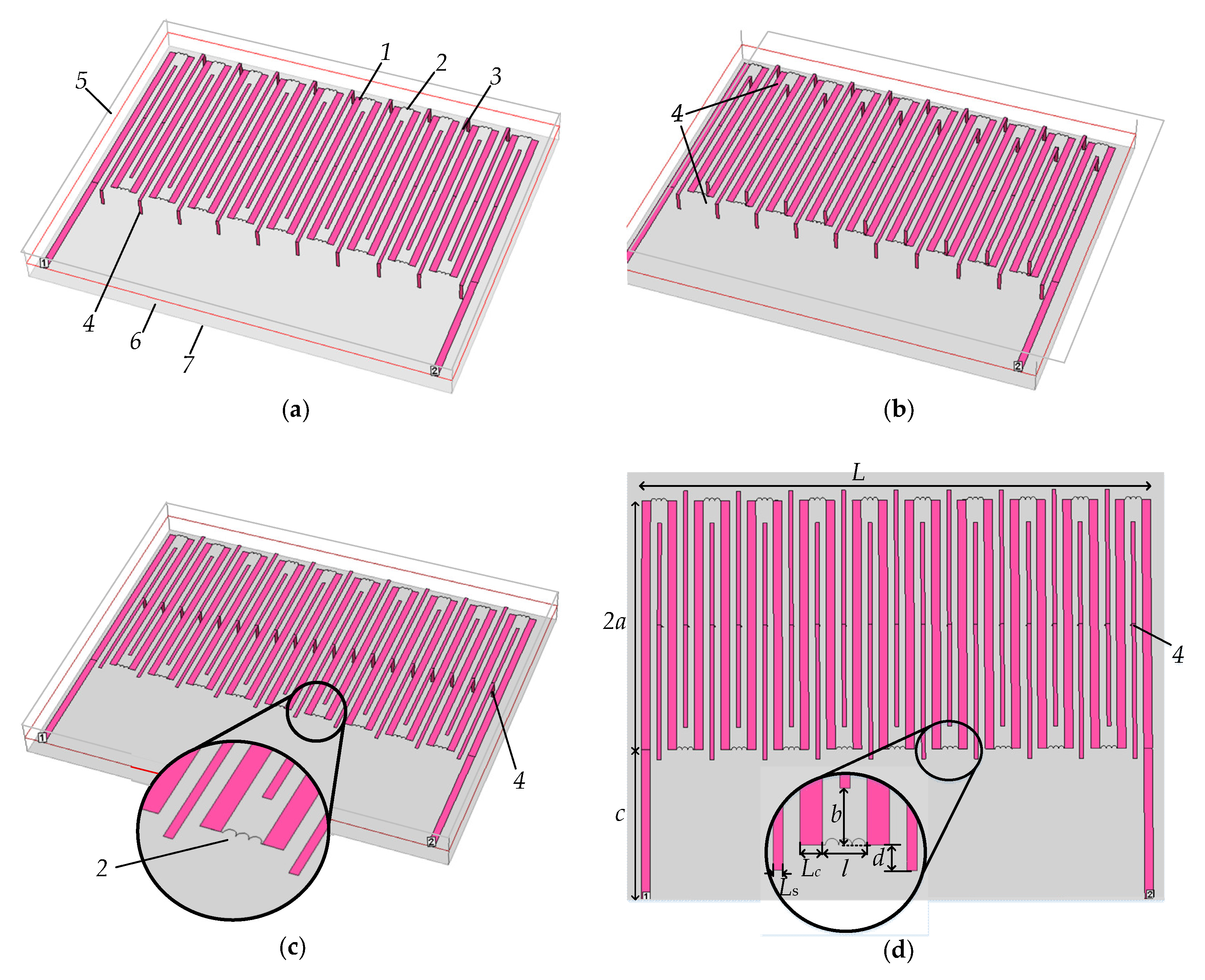
Models of the hybrid meander structure with additional shields and different grounding positions are presented in
Figure 1. First of all, these models were designed in the Sonnet
® commercial software package. The main dimensions of the meander structure with additional shields were as follows: the length of the hybrid meander structure,
L = 20.28 mm; the width of the hybrid meander structure, 2
a = 10 mm; the length of the additional electrodes,
c = 6 mm; the width of the meander electrode,
Lc = 0.35 mm; the gap between adjacent conductors,
l = 0.7 mm; the width of the shields,
Ls = 0.15; the thickness of the substrate,
hs = 0.2 mm; the thickness of the conductors,
hc = 0.035 mm. An FR4 material was used for the substrate where
εr = 4.8 and tanδ = 0.02. Copper was used for the conductor, whose inductivity was equal to 5.8 × 10
7 S/m.
A model of the hybrid meander structure with grounding in one end of the additional shields is presented in
Figure 1a. The grounding in both ends of the additional shields is presented in
Figure 1b. The grounding only in the middle of the additional shields is presented in
Figure 1c. A 2D top view of the hybrid meander structure with additional shields, which are grounded in the middle, is presented in
Figure 1d. The connecting electrodes of the meander were replaced with the lumped inductive elements in the peripheral parts of the meander. A zoomed lumped inductive element is shown in
Figure 1d.
The hybrid meander structure was estimated based on the S21 transmission and S11 reflection parameters. In addition, input impedance ZIN and delay time td characteristics were presented during the investigation. The values of the inductive components were changed from 1 to 10 nH with a step of 1 nH.
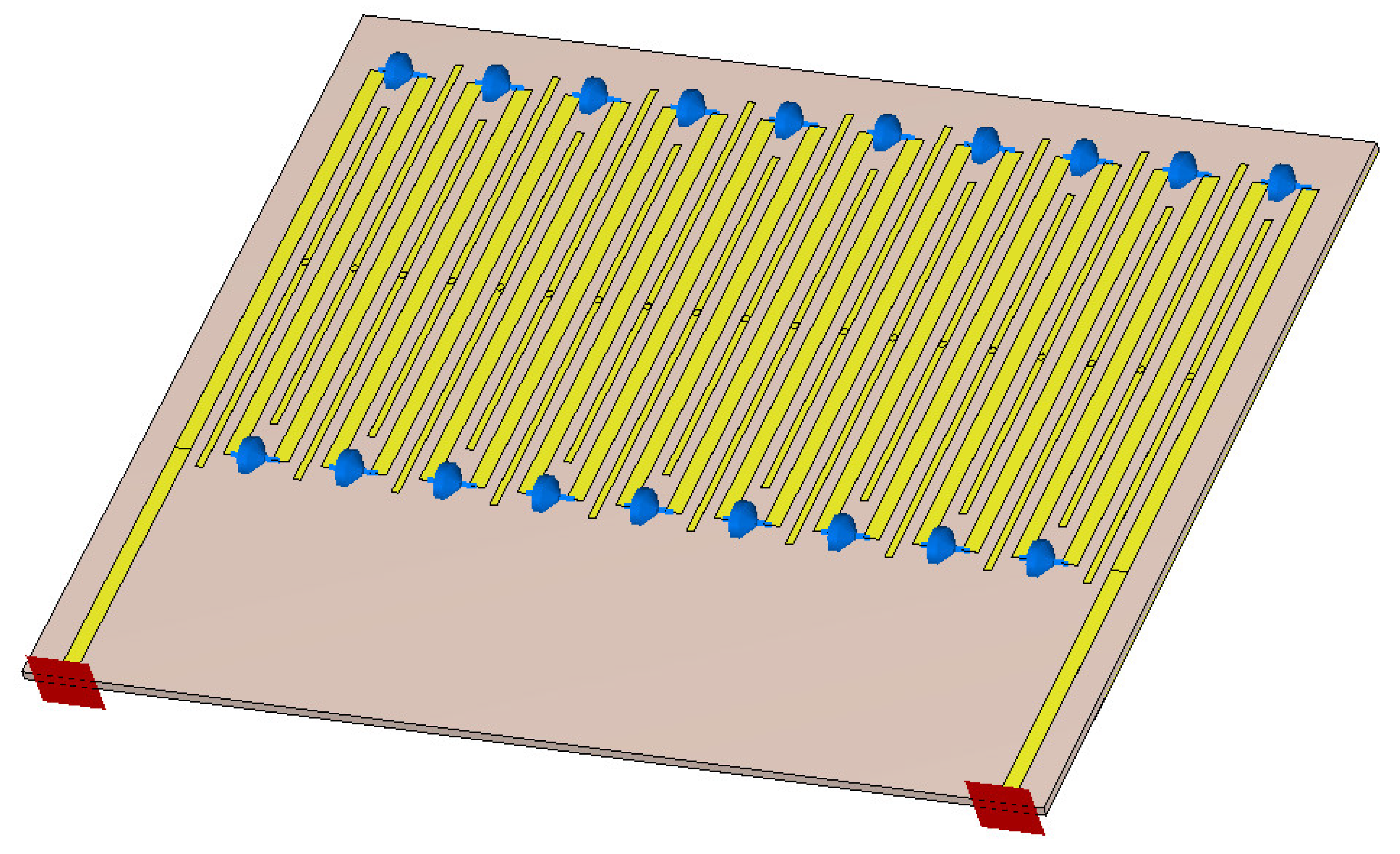
The computer-based modeling was also repeated in the CST Microwave Studio
® commercial software package, which is based on the finite-difference time-domain method. The hybrid meander structure with additional shields, which are grounded in the middle, is presented in
Figure 2.
The same design and material parameters were maintained as in the Sonnet® software package. All the design and material parameters during the computer-based modeling were selected based on the ability to repeat the experiment physically.
2.2. Models for Experimental Investigation
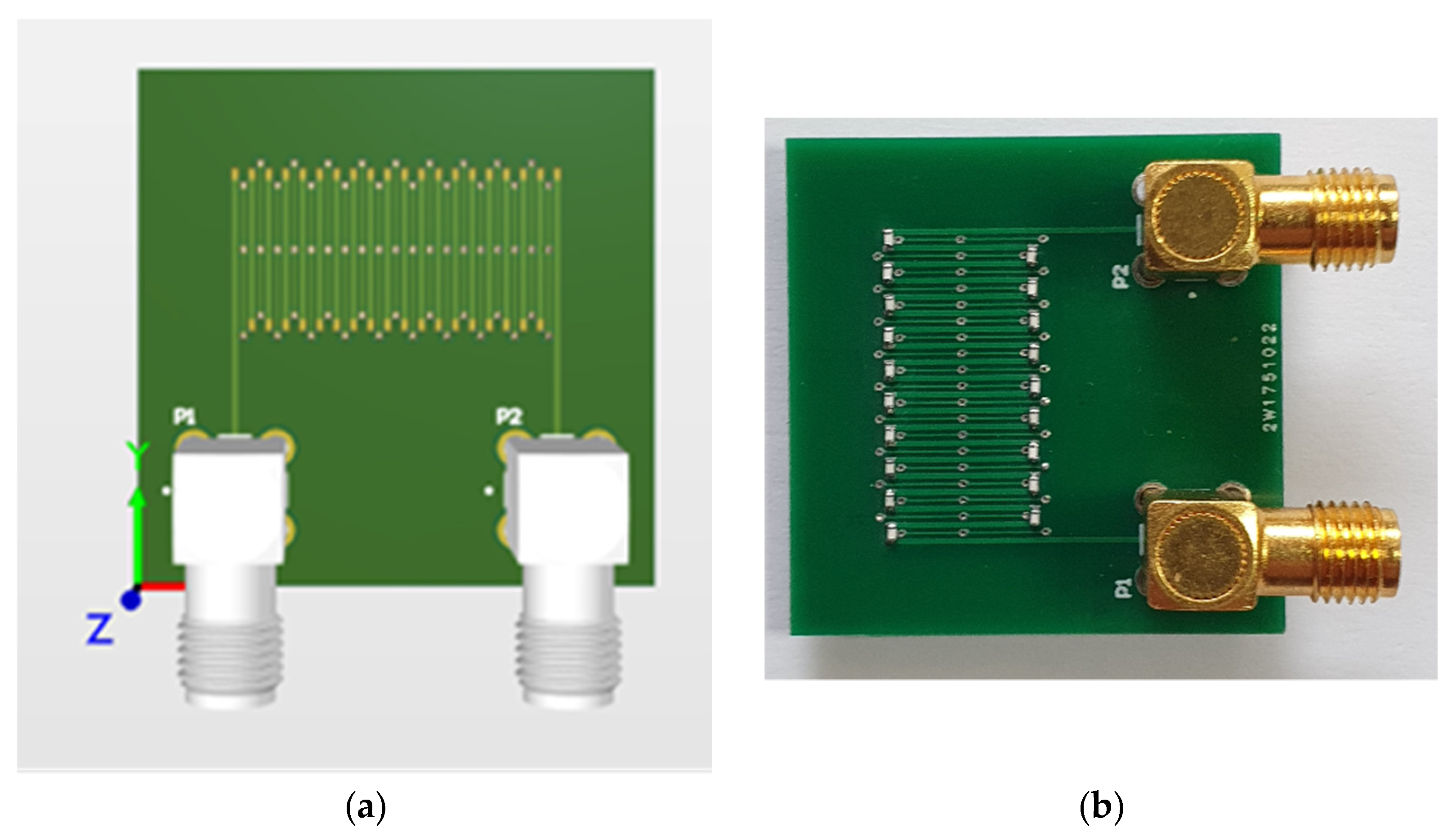
The PCB of the hybrid meander structure was designed in the Altium Designer® (Altium Designer 2010, Altium, La Jolla, CA, USA, 2010) software package. The design parameters were used similarly as in the modeling procedure. To be more precise, the design parameters were taken into account during the computer-based modeling stage according to recommendations from the manufacturer about minimal possible sizes and materials.
The contact plates, which represent the positions of the lumped inductive elements, are presented in
Figure 3a. Positions of vias in the middle and ends of the additional shields are drilled and visible in the top-view PCB image. The universal PCB is prepared with all holes already drilled in the factory.
The overall dimensions of the prototype plate were 32 × 32 mm
2. All other parameters were the same as in the modeling procedure. The length of the hybrid meander structure was
L = 20.28 mm, the width 2
a = 10 mm, the length of the additional electrodes
c = 6 mm, the width of the meander electrode
Lc = 0.35 mm, the gap between adjacent conductors
l = 0.7 mm, the width of the shields
Ls = 0.15, the thickness of the substrate
hs = 0.2 mm, and the thickness of the conductors
hc = 0.035 mm. An FR4 Kingboard tg150 material was used for the substrate where
εr = 4.8 and tanδ = 0.02. Copper was used for the conductor, whose inductivity was 5.8 × 10
7 S/m. The diameter of the drilled holes was 0.3 mm. The manufactured prototype of the hybrid meander structure is presented in
Figure 3b. SMA connectors were used for the connection.
Two different types of ground metallization were used during the physical investigation. The first variant was made when the grounding was in the middle of the additional shields. The second variant was when the grounding was in both ends of the additional shields of the hybrid meander structure.
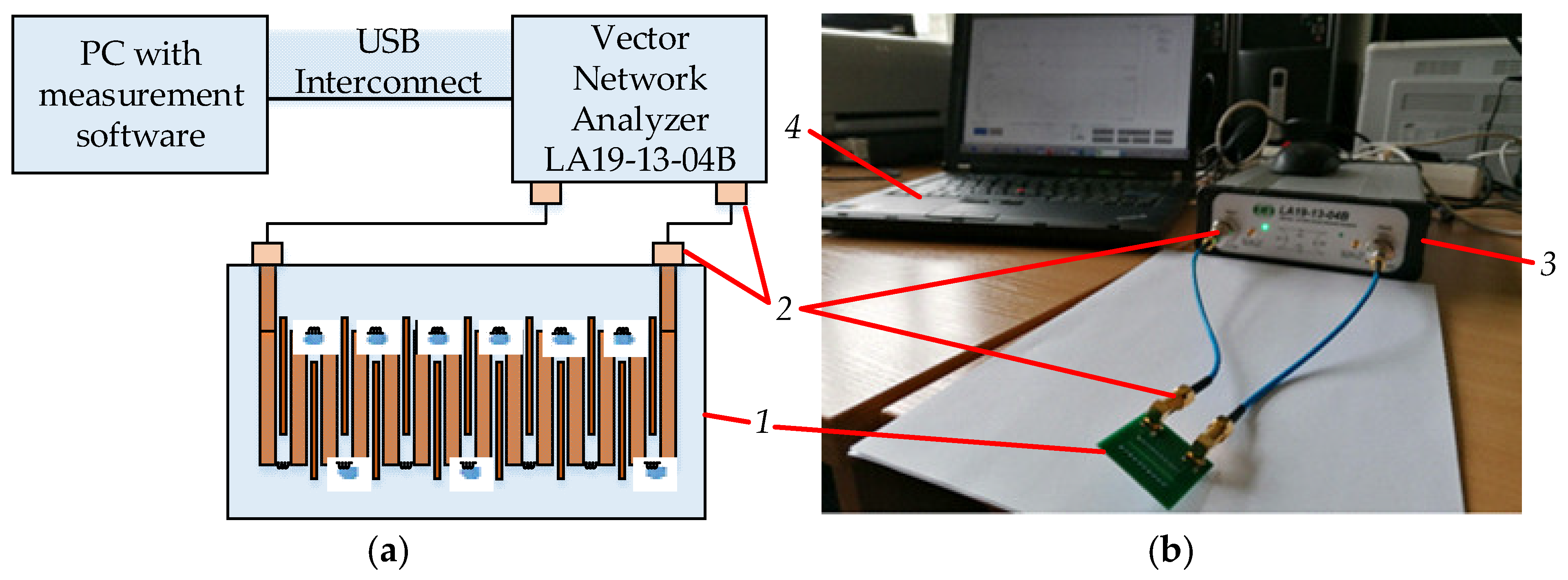
Prototypes with different values of the lumped inductive elements were made. Prototypes with 1 nH, 5.1 nH, and 10 nH elements are presented for discussion. SMD inductors of a 0402 case were used. The S
11 reflection and S
21 transmission parameters were measured using an LA19-13-04A vector network analyzer (VNA). The delay time
td characteristic was calculated from S
21 phase characteristics. A block diagram of an experimental measurement of the hybrid meander structure is presented in
Figure 4a. A general photograph of the experiment is presented in
Figure 4b.
An LA19-13-04A vector analyzer has an 8.5 GHz frequency range and is capable of measuring the required S parameters. The calibration phase and obtaining of the results were performed using the recommendations of the manufacturer.
3. Results
Models of the hybrid meander structures were investigated by computer-based modeling using the Sonnet® and CST Microwave Studio® commercial software packages. The results of the computer-based modeling were compared with the results of the physical experiment.
3.1. Results of Computer-Based Modelling
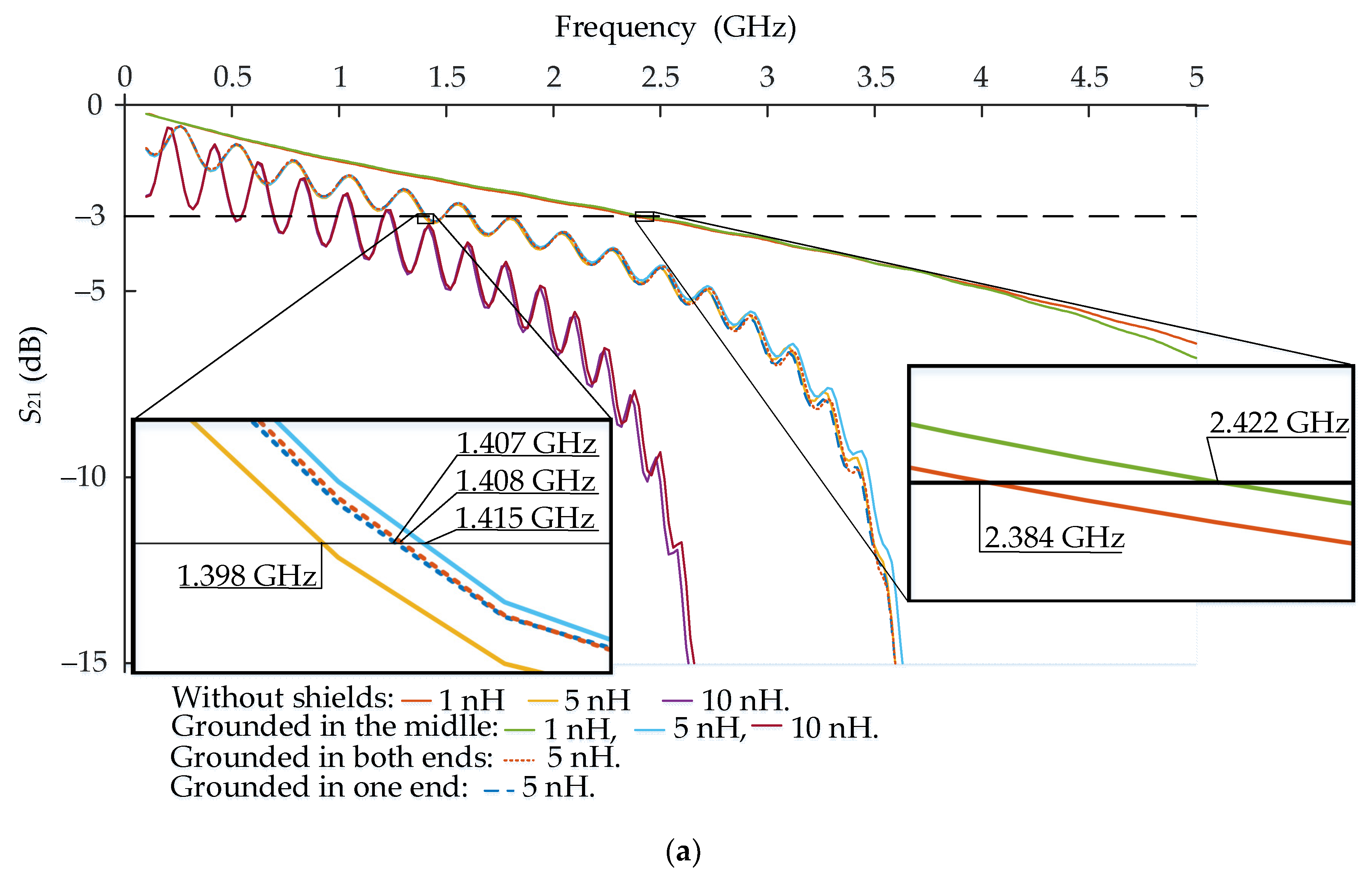
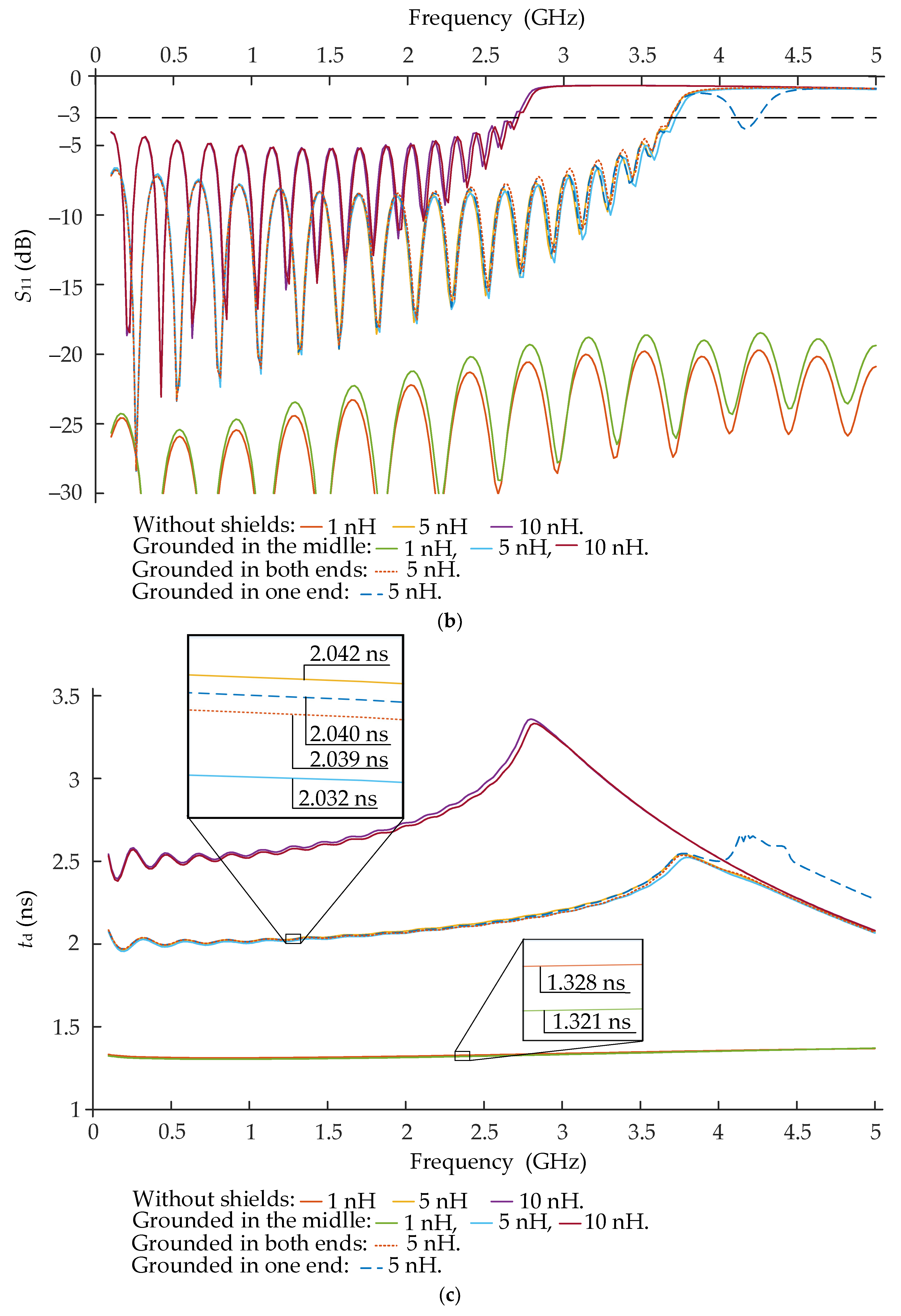
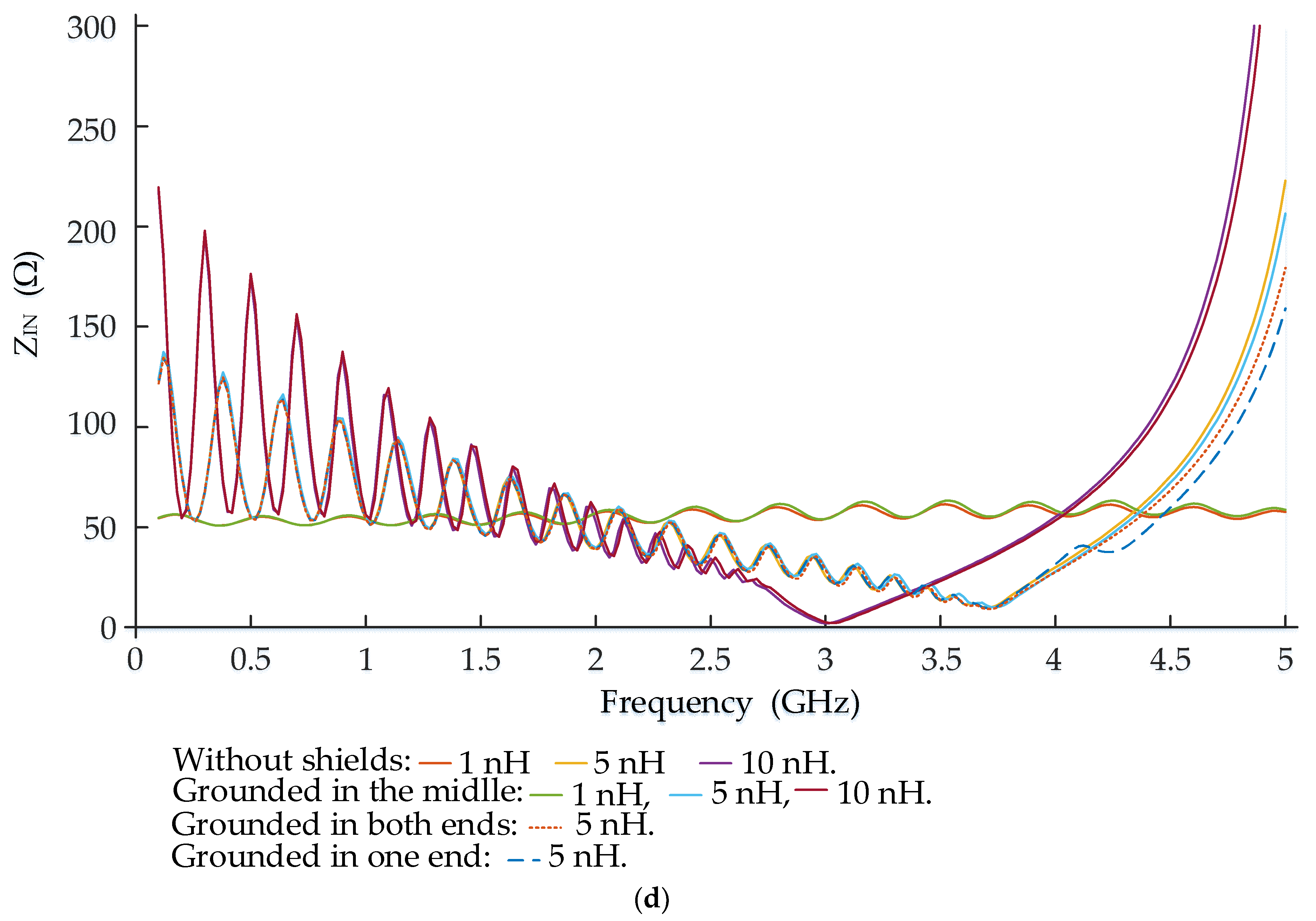
A comparison of the results of the hybrid meander structures without and with additional shields is presented in
Figure 5. The results of the S
11, S
21,
td, and
ZIN characteristics were obtained using the computer-based modeling in the Sonnet
® software package.
First, a comparison was performed when the values of the lumped inductive elements varied and were equal to 1 nH, 5 nH, and 10 nH, while the grounding position was in the middle. Second, the influence of the grounding positions was investigated with the constant 5 nH lumped elements and grounding positions in the middle, one end, and both ends of the additional shields.
First of all, the results confirm that the inductance of lumped elements affects the passband of the hybrid meander structure. The cutoff frequency is 2.384 GHz when 1 nH lumped inductive elements are used. The passband is 1.398 GHz when 5 nH lumped inductive elements are used. The passband decreases to 0.508 GHz when 10 nH lumped inductive elements are used. These changes are clearly visible in the 5 GHz frequency range in
Figure 5a. The curves without and with additional shields and with the same inductance of lumped elements almost overlap. Therefore, the groups of curves with the same 1 nH and 5 nH inductances of lumped elements are zoomed near the cutoff frequencies for better visibility.
Moreover, the passband varied by no more than 38 MHz when models of the hybrid meander structures with and without additional shields were compared. For example, the passband was increased by 38 MHz up to 2.422 GHz when the additional shields were added to the hybrid meander structure with 1 nH lumped elements. This is an improvement of about 1.6% when compared with the overall passband of the hybrid meander structure. The improvement of the passband decreases when the inductance of lumped elements increases. The passband was increased only by 17 MHz up to 1.415 GHz when 5 nH lumped elements were used. This is an improvement of about 1.2%. The case with 10 nH lumped elements showed an improvement of only 7 MHz, but this variant is not zoomed in
Figure 5a.
The influence of the grounding positions of the additional shields on the passband of the hybrid meander structure was investigated when 5 nH lumped elements were used. The best results with a 17 MHz improvement up to 1.415 GHz were obtained when the additional shields were grounded in the middle. The grounding in both ends of the additional shields gave a 10 MHz improvement. The worst result with a 9 MHz improvement was obtained when the additional shields were grounded only in one end.
The results also confirm that the delay time td depends on the value of the inductivity of lumped elements. A positive feature is that the inductive lumped elements allow for changing the delay time without changing the dimensions of the hybrid meander structure. In this particular case study, if the delay time is equal to 1.321 ns, then the inductivity is equal to 1 nH. The delay time increases more than twice to 2.5 ns when the inductivity increases to 10 nH. The delay time is almost constant in the entire frequency range when 1 nH lumped elements are used.
The additional shields also effected the delay time characteristic. The td decreased by 7 ps at a 2.422 GHz cutoff frequency when 1 nH lumped elements were used. The td decreased by 10 ps at a 1.412 GHz cutoff frequency when 5 nH lumped elements were used. In both cases, the shields were grounded in the middle. The grounding position in one or both ends of the additional shields gave decreases of delay time by 3 and 2 ps, respectively, when 5 nH lumped elements were used.
To sum up, the additional shields and their grounding positions had an impact on the frequency characteristics of the hybrid meander structure. On the other hand, the impact was very small and not as clearly visible as in the planar meander structures. The computer-based modeling using Sonnet® showed that a variation in the inductance of lumped elements in the range of 1 to 10 nH allows for changing the width of the passband only in the range of 1.6%.
We think that the main reason for this is that the lumped inductive elements affect the characteristic impedance of the line, and there is no more matching between the meander line, generator, and load resistors. With the initial design parameters without the lumped elements, the characteristic impedance was matched to the generator and load resistors and was 50 Ω. The broken matching condition can be seen from the
S11 reflection parameter in
Figure 5b and the input impedance parameter in
Figure 5d. The input impedance is higher in lower frequencies up to 2 GHz. The input impedance decreases with an increase in frequency until the stop band appears. The fluctuation of the input impedance is bigger in lower frequencies.
3.2. Results of Physical Experiment
The computer-based modeling was also repeated in the CST Microwave Studio
® software package before moving to the physical experiment. The experimental investigation was made according to the PCB and prototype, which are presented in
Figure 3. The procedure for the measurements is discussed in the previous section in
Figure 4.
The computer-based modeling and measurements were repeated many times with different initial parameters of lumped elements and grounding positions of the additional shields. Results, which were obtained using the computer-based modeling in Sonnet
® and CST Microwave Studio
®, were verified by the physical experiment. For clarity, the computer-based modeling and experimental results are compared by presenting only one separated case in
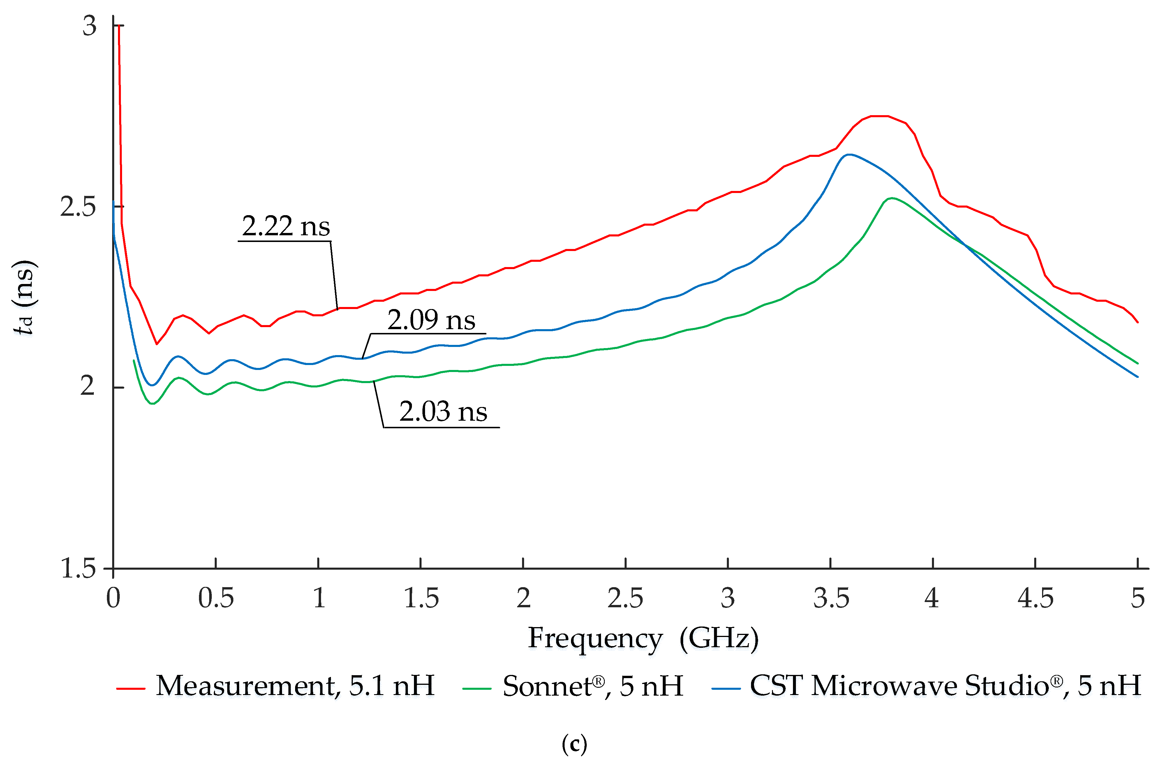
Figure 6. The inductivity of lumped elements was 5 nH, and the additional shields were grounded in the middle position in this separated case. This case summarizes and perfectly reflects all the other cases during the investigation.
The results of S
21 are presented in
Figure 6a. The cutoff frequency of the physical experiment with 5 nH lumped elements is 1.17 GHz. This is less by 180 MHz in comparison with the results obtained using CST Microwave Studio
® and less by 240 MHz in comparison with the results obtained using Sonnet
®. The differences between the results become smaller when the inductance of lumped elements increases.
The results of the delay time characteristic are presented in
Figure 6c. The
td was 2.22 ns at a 1.17 GHz cutoff frequency during the physical experiment. The
td = 2.09 ns was obtained in CST Microwave Studio
® at a 1.35 GHz cutoff frequency and the
td = 2.03 ns in Sonnet
® at a 1.41 GHz cutoff frequency.
ZIN was not included in the comparison because the influence of the additional shields and their grounding positions on the frequency characteristics of the hybrid meander structure was seen from the S
11 and S
21 parameters and
td characteristic.
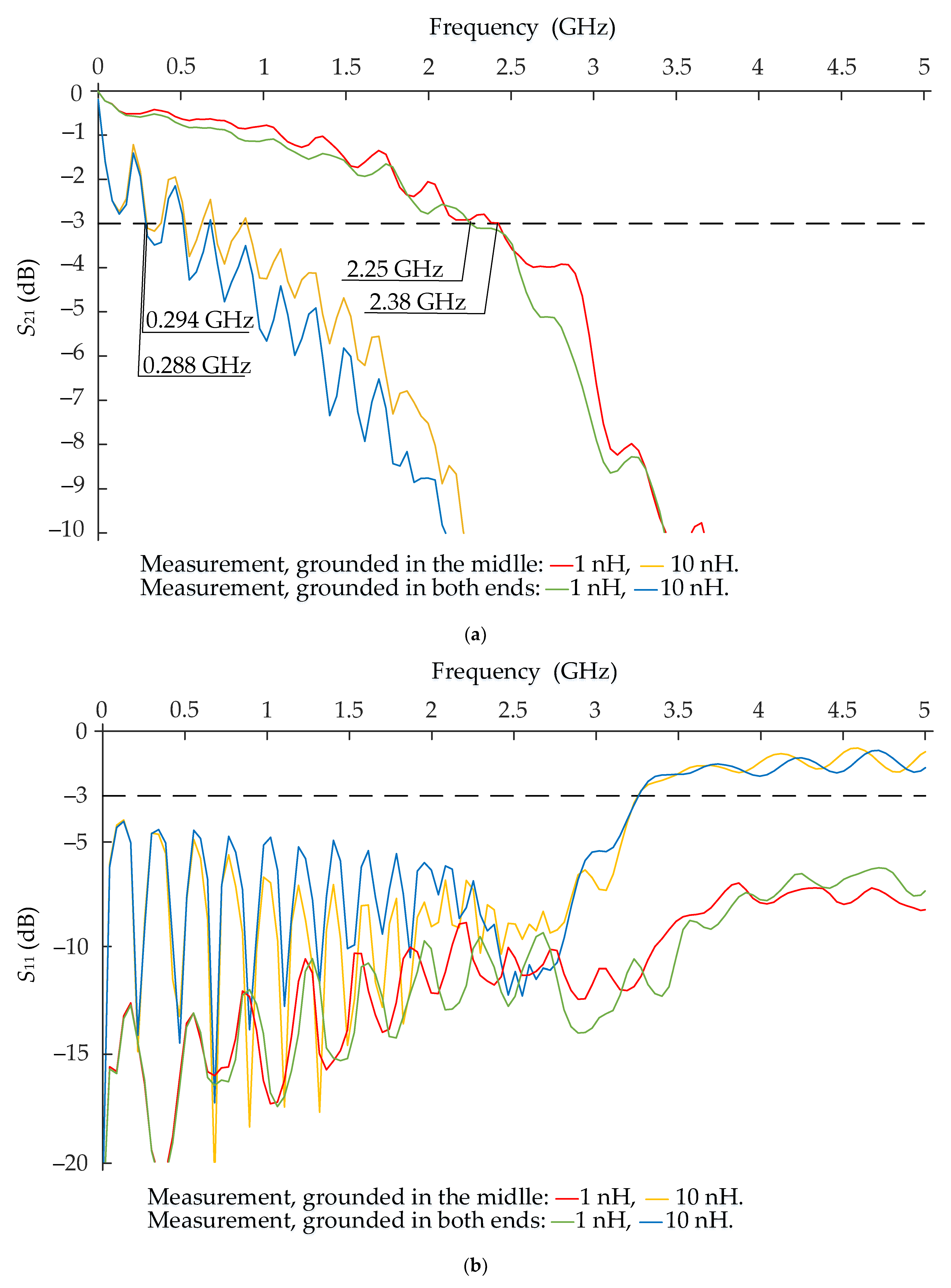
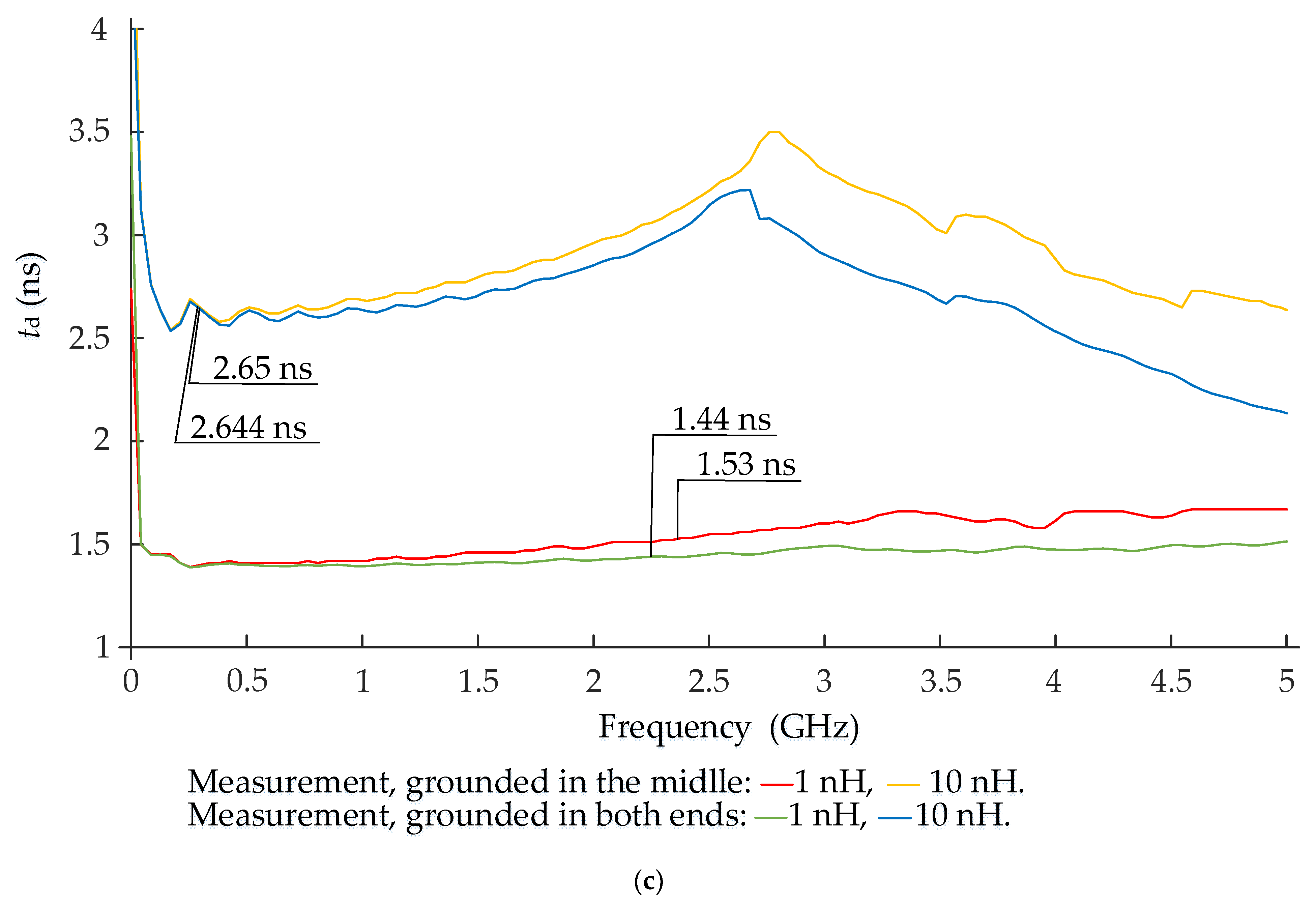
All the results that were obtained with the computer-based modeling and the physical experiment correlate with each other. Only the additional two cases with the results of the measurement are presented in
Figure 7 in order to reveal the influence of grounding positions on the additional shields.
The results of S
21 when the grounding position is in the middle or in both ends of the additional shields are presented in
Figure 7a. The cutoff frequency is higher by 130 MHz and is 2.38 GHz when the additional shields are grounded in the middle in the case with 1 nH lumped element. The difference is only 6 MHz in the case when 10 nH lumped elements are used. The
td is higher by 90 ps and is 1.53 ns when the grounding position of the additional shields is in the middle when 1 nH lumped elements are used. The results of the measurements confirmed the results of the computer-based modeling. The higher the inductance is in the lumped elements, the lower the influence of the additional shields and their grounding positions is.
4. Discussion
Our previous research showed positive features where lumped inductive elements allow the increase of the values of the input impedance and delay time without changing the dimensions of the overall structure. On the other hand, such hybrid systems would also have negative properties. Increasing the inductance at the edges of the meander line reduces the passband because of the matching issues between the line impedance and the generator and load resistors. In some cases, for example, in planar meander structures, the coupling between adjacent conductors could be reduced by using additional shields. Therefore, it was necessary to research the influence of additional shields and their grounding positions on the frequency characteristics of the hybrid meander structures.
The results, which were presented in the previous section, showed that it is possible to adjust the operation of the hybrid meander structure by replacing the connecting electrodes with lumped inductive elements. The delay time could be controlled by varying the inductance of lumped elements without the need to change the dimensions of the hybrid meander structure. In our experiment, the delay time varied by approximately 1.2 ns in the range of 1.3 to 2.5 ns when the inductance was changed from 1 to 10 nH.
On the other hand, the increase in inductance in lumped elements decreased the passband. The additional shields had an impact and increased the passband, but the increase was not significant. The improvement of the passband was no more than 1.6% when compared with the overall passband of the hybrid meander structure in our measurements. The grounding position of the additional shields also had a small impact on the operation of the hybrid meander structure. The greatest impact was obtained when the grounding was in the middle. The grounding in one end only showed the worst results.
In summary, the properties of the hybrid meander structure with additional shields were revealed. The results of the computer-based modeling and the physical experiment correlated both qualitatively and quantitatively.


