1. Introduction
Modern high-performance microprocessors feature tens of processor cores [
1], operate with clock frequencies up to
[
2], and, with this, achieve previously unmatched computational performance. However, this performance increase is accompanied by an increase of the required power, which can exceed
per device [
3]. In this context, the concept of Dynamic Voltage and Frequency Scaling (DVFS), in combination with a granular power delivery system that features independent Voltage Domains (VDs) for different cores or parts of cores, can achieve an effective reduction of the power demand [
4]. By way of example, it was found in [
5] that a video decoder test chip, which employs multiple different VDs with configurable supply voltages (two defined voltages:
and
), can achieve a reduction of the supplied power by 55% to 61%. In addition, it is desirable to reduce the high package currents of modern microprocessors. Reduced package current and adjustable supply voltages for the different VDs can be achieved with buck-type Integrated Voltage Regulators (IVRs) that are located in the package of the microprocessor or on the microprocessor die [
6].
Table 1 summarizes the main specifications of the considered IVR.
Common topologies for IVRs are Switched Capacitor Converters (SCCs) and buck converters with output inductors. Numerous examples of SCCs are documented in the literature, e.g., a standalone SCC topology with regulated output voltage (using pulse frequency modulation) [
7], an SCC with a low dropout regulator in parallel to achieve low output voltage ripple [
8], and a hybrid DC–DC converter, which comprises a 2:1 SCC and a
output inductor to achieve soft switching in order to increase the efficiency of the SCC [
9]. The absence of inductors renders SCC topologies attractive with regard to chip integration, to avoid the challenges related to magnetic components (losses and required footprint area [
10], the integration of magnetic materials [
11], and, depending on the realization, the need for through silicon vias [
12]). However, the topologies of SCCs are subject to a predefined voltage conversion ratio and generate increased losses when operated with input-to-output voltage ratios that deviate from the predefined ratio (for example, this can be observed in Figure 6 in [
7], which depicts efficiency curves for an input voltage of
and output voltages ranging from
down to
). Accordingly, inductor-type buck converters are often preferred if the ratio of input-to-output voltage is variable. Documented realizations include multi-phase buck converters with on-die inductors with a magnetic core [
12], on-package air core inductors [
13], and discrete inductors [
6]. In addition, numerous improvements have been presented in the literature, e.g., the use of discontinuous conduction mode [
14] and the implementation of a small SCC that is connected in parallel to the output of the buck converter [
15], to achieve increased efficiencies under medium- and light-load conditions, respectively.
This paper presents an evaluation of an inductor-based buck-type IVR, whose power stage is comprised of four converter phases (half-bridges) that are operated in parallel with interleaving. The power stage was implemented in the high-end
CMOS technology node of the microprocessor, in order to allow for on-die integration, and employed short-channel transistors, instead of long-channel devices, to take advantage of their low conduction and switching losses [
16]. With this, a high switching frequency of up to
can be achieved, which enables a fast transient response that is needed for microprocessor applications [
17]. However, short-channel transistors are subject to a reduced breakdown voltage. For this reason, the power switches of each half-bridge were realized with stacked transistors (CMOS Half-Bridges with Stacked Transistors (HBSTs)) [
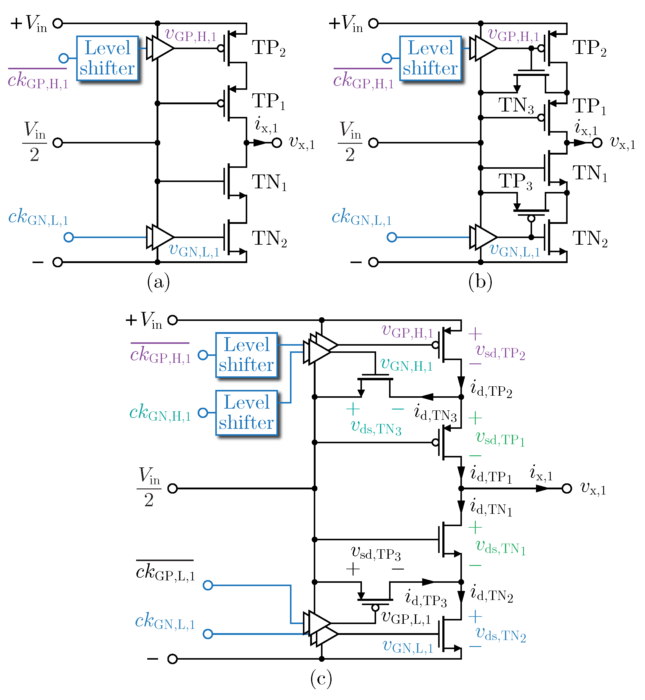
18], depicted in
Figure 1a, in order to reduce the voltage applied to each power transistor to half of the input voltage of the CMOS HBST. (Please note that all circuits depicted in
Figure 1 refer to Phase 1 of the four-phase IVR and include level-shifters, which are needed to provide the correct voltage levels for the gate drivers connected to
and
.)
The CMOS HBST has been used in IVRs of commercial microprocessors in modern technology nodes built in the most recent tri-gate technology nodes, e.g.,
[
13] and
[
19]. Although, high efficiencies are achievable using the CMOS HBST, e.g., 88% in [
14], the blocking voltages of the stacked transistors can be unequal, which leads to reduced reliability and increased losses [
20]. To achieve equal blocking voltages, the CMOS HBST with Active Neutral Point Clamping (CMOS ANPC HBST), depicted in
Figure 1b, was considered, which adds clamp switches to the CMOS HBST to actively clamp the potential between the stacked transistors to a middle potential [
21]. The CMOS ANPC HBST uses common gate drivers for the main switches and the respective clamp switches. Therefore, the clamp switches
and
are both turned on if
and
are both turned off. In addition,
starts to conduct if its gate-to-drain voltage is less than
and
starts to conduct for a gate-to-drain voltage higher than
, which is found in
Section 2, in the course of the investigation of the simulation results. For this reason, the output of the power stage cannot be switched to high impedance. Accordingly, phase shedding, which is used to increase part-load efficiency in multi-phase converters [
22], is not possible. The CMOS ANPC HBST with Independent Clamp Switches (ICSs) of
Figure 1c eliminates this shortcoming by using separate gate drivers for the clamp switches [
20]. Please note that
Figure 1c defines all currents and voltages of the waveforms discussed in
Section 2. Furthermore, the symbols
,
,
, and
in
Figure 1c refer to digital gate signals that stem from the circuitry explained in
Section 3.
The three investigated topologies, HBST, ANPC HBST, and ANPC HBST with ICS, mainly differ with regard to their behavior during switching. Accordingly, the switching operations are inspected in a first step in
Section 2 based on simulation results in order to gain a deeper understanding of the different topologies. However, the conducted simulations disregard different loss components, e.g., due to the Power Distribution Network (PDN) and the metal layers of the chip. In order to provide a robust comparison of the three topologies, experimental efficiency results are used to assess the topologies. In this regard,
Section 3 summarizes the implementation details of the realized IVR.
Section 4 presents the results of the experimental evaluation.
Section 5 provides a final discussion. With this, the paper provides the two key contributions listed below.
- (1)
first, the experimental validation of a CMOS ANPC HBST with ICS that is realized in CMOS technology;
- (2)
a comparative evaluation of the conventional CMOS HBST, the conventional CMOS HBST ANPC, and the CMOS HBST ANPC with ICS based on measured efficiencies.
2. Investigation of the Switching Operations
This section investigates the switching operations of the three considered circuit topologies, i.e., the CMOS HBST in
Section 2.1 and the CMOS ANPC HBST, as well as the CMOS ANPC HBST with ICS in
Section 2.2, using simulated waveforms, and presents a related discussion of the main findings in
Section 2.3. All simulations were conducted with the circuit simulator that is part of the Virtuoso Custom IC Design Environment by Cadence (Version ICADV12.1), which, for the employed
CMOS technology, was the only software tool for simulation that was available to our research group in the scope of this work. By way of example, Converter Phase 1 of the four-phase IVR was selected for this purpose. With this, it provides a knowledge basis for the discussions presented in the subsequent sections of this paper. This section summarizes the findings of a previous conference publication [
20].
Figure 2 presents typical gate voltages that are used to generate an output voltage,
, with a defined duty cycle at the switching node of the buck converter.
Figure 2a depicts the gate voltages
and
that are applied to the transistors
and
, respectively. These waveforms are valid for all three topologies shown in
Figure 1.
Figure 2b shows the additional gate voltages,
and
, for the clamping switches
and
of the CMOS ANPC HBST with ICS. The presented gate voltages are measured with respect to the minus terminal of the power stage. (Please note that
,
, and
are p-type MOSFETs; for this reason, negative gate-to-source voltages are needed to turn on
,
, and
. In addition, the gate voltages of
and
,
and
, feature an offset of
, which is needed to keep the transistors’ gate-to-source voltages within the allowable voltage range.) In the case of the CMOS HBST, solely the switching states of
and
determine the switching states of
and
, respectively, e.g., if
is in the on-state and
in the off-state (with an assumed drain-to-source voltage of
), the gate-to-source voltages of
and
are equal to
and zero, respectively. Accordingly,
is in the on-state and
in the off-state.
Figure 2a,b reveals the dead times between subsequent turn-off and turn-on events, to avoid short-time short circuits in the HBST, and
Figure 2c illustrates the waveform of the voltage at the switching node,
, that results for the gate voltages of
Figure 2a (and
Figure 2b in the case of the CMOS ANPC HBST with ICS) and a positive output current,
. During the voltage transitions between zero and
, the actual waveform of the switched voltage depends on the topology as explained in
Section 2.1 and
Section 2.2.
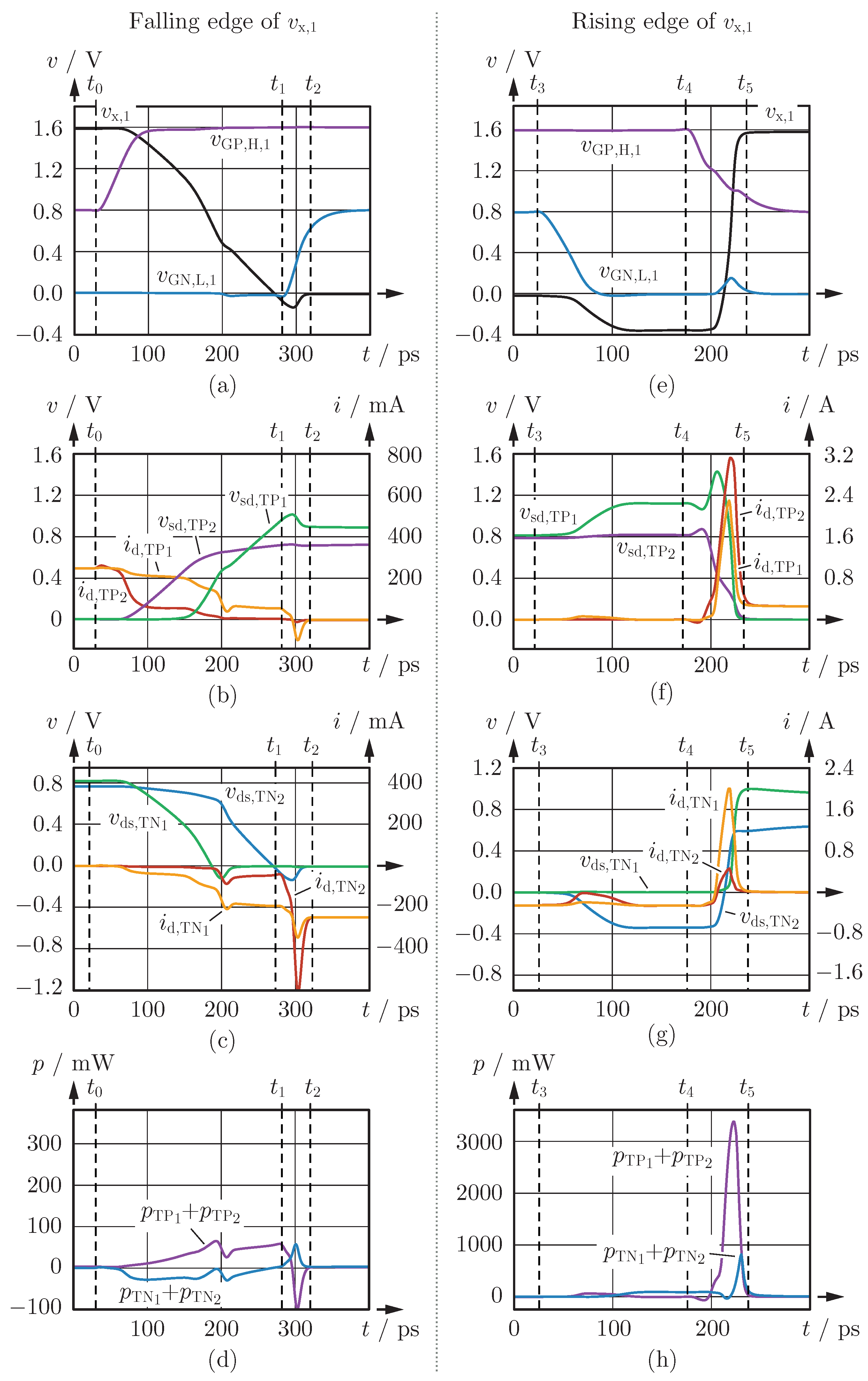
The simulated waveforms of the transistor currents and drain-source voltages during the time intervals where
changes from
to zero and vice versa are presented in
Figure 3,
Figure 4 and
Figure 5 for the CMOS HBST, the CMOS ANPC HBST, and the CMOS ANPC HBST with ICS topologies, respectively. All simulations considered the settings of
Table 1 and a constant output current of
(i.e., a negligible output current ripple was assumed) and disregarded the implications of the metal layers and the power distribution network of the IVR’s Power Management IC (PMIC) on the waveforms.
2.1. Conventional HBST
The conventional
CMOS HBST is considered in a first step. In the case of a falling edge of
, first,
is commanded to switch off at
, as shown in
Figure 3a (please note that the definitions of all currents and voltages used in
Figure 3 are given in
Figure 1c). The constant output current charges the output capacitance of
, and
increases, which is depicted in
Figure 3b. As a consequence, the gate-to-source capacitance of
is discharged, and subsequently,
is turned off. With increasing source-to-drain voltages of
and
, the drain-to-source voltages of
and
decrease, as shown in
Figure 3c, in order to keep the sum
equal to the input voltage. Accordingly, very small turn-on losses can be achieved during
, if the dead time is sufficiently large, such that
and
reach zero before
is commanded to turn on at
.
Figure 3d depicts the instantaneous losses of the four power transistors, that is the products of drain-source voltages and drain currents (not considering the gate driver losses). This result reveals that a large part of the stored energy can be recycled, leading to low total switching losses. However, after the switching operation has elapsed, for
, the simulation computes unequal source-to-drain voltages for
and
, i.e.,
applies.
The rising edge of
is initiated by commanding
to turn off at
, which is depicted in
Figure 3e. During the dead time interval,
,
remains in the on-state, and the high-side transistors
and
remain off. As a consequence,
conducts the output current,
, which charges the output capacitance of
until
reaches approximately
; cf.
Figure 3g. With this, the gate-to-drain voltage of
,
, reaches approximately
, which leads to a turn-on of
, i.e.,
conducts the output current. As a result, increased conduction losses occur in
during the dead time. Furthermore, the negative value of
leads to an overvoltage condition for
. (The current that charges the output capacitance of
,
in
Figure 3g, finds a low impedance path (to
) in the large input capacitance of
. For this reason, only negligible charging current remains for
, leading to a negligible overvoltage across
during the dead time interval.) At
,
is commanded to turn on. The associated turn-on processes force
and
to decrease to zero, as shown in
Figure 3f. During turn-on, large spikes are observed in the drain currents of
,
, and
.
Figure 3h depicts the instantaneous losses in the transistors, which are particularly high for
and
. According to
Figure 3g,
and
are subject to unequal drain-to-source voltages after the switching operation has elapsed, i.e., for
.
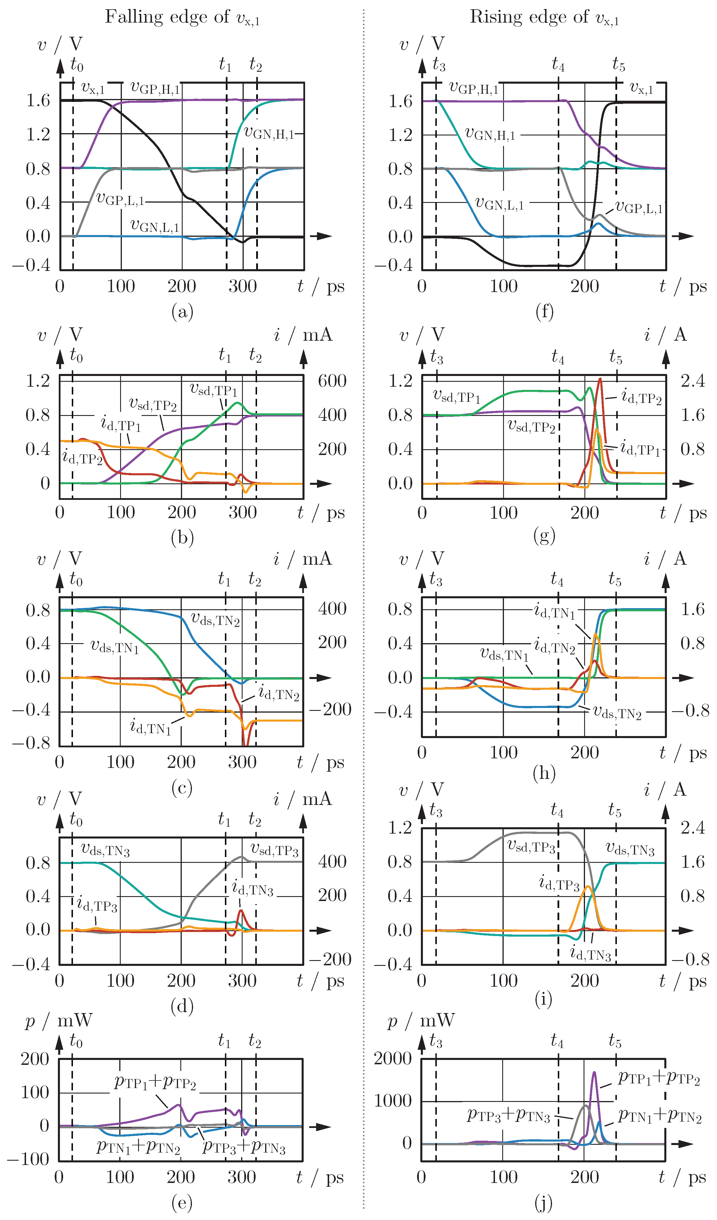
2.2. ANPC HBST without and with ICS
Figure 4 depicts the transistors’ currents and voltages that result for the
CMOS ANPC HBST for a falling edge of
in
Figure 4a–e and a rising edge of
in
Figure 4f–j.
Figure 4 depicts the waveforms of the same physical variables as
Figure 3 and, in addition, also shows the drain-to-source voltages and the drain currents of the clamping switches,
and
in
Figure 4d,i. Compared to the CMOS HBST, the clamping switches
and
are both turned on during the dead time and define the drain potentials of
and
during this time.
In case of a negative slope of
, the turn-on of
leads to increased switching losses during
and the turn-on of
to increased switching losses during
. In addition, an increased forward voltage drop across
, which conducts the output current during the dead time, of
, is found during
, which leads to increased conduction losses during this time interval. (The constant output current charges the output capacitance of
until
applies, which increases the gate-to-drain voltage of
to approximately
, since
is turned on. As a consequence,
is forced to conduct the output current (via
) during the dead time interval,
.) In the case of a positive slope of
, the turn-on losses are found to be less than for the HBST topology, because the active clamp switches enforce a reduction of
during the dead time
, which also decreases the value of
during the turn-on time interval,
, as shown in
Figure 4g. Furthermore, equal blocking voltages are achieved after both switching operations, i.e.,
for
in
Figure 4b and
for
in
Figure 4h.
The waveforms of the transistor voltages and currents simulated for the
CMOS ANPC HBST with ICS are depicted in
Figure 5. Compared to the CMOS ANPC HBST without ICS, the main switches and the clamp switches are commanded to turn off during every dead time. This can be seen in
Figure 5a,f, which presents the transistors’ gate signals for a falling and a rising edge of
, respectively. For this reason, the switching operations are the same as for the conventional HBST described in
Section 2.1 during
and
. However, at the end of the dead time interval, either
(at
in
Figure 5a) or
(at
in
Figure 5f) is turned on in addition to the two main switches (
and
or
and
, respectively). With this, equal drain-to-source voltages of the main power switches are enforced as soon as the respective clamp switch is in the on-state, i.e., for
in
Figure 5b and for
in
Figure 5h.
2.3. Discussion
A comparison of the instantaneous switching losses during the rising edge of
of the ANPC HBST without and with ICS revealed lower losses of
for the ANPC HBST without ICS, compared to
for the ANPC HBST with ICS (for the instantaneous power waveforms depicted in
Figure 4j and
Figure 5j). However, in the case of a falling edge of
, the ANPC HBST without ICS is subject to higher losses of
(
Figure 4e), compared to
for the ANPC HBST with ICS (
Figure 5e). In addition, the switching losses depend on the dead times,
and
. Accordingly, it is not directly possible to draw a meaningful conclusion. For this reason, the characteristics of the overall simulated efficiencies of the three investigated topologies are compared to each other in
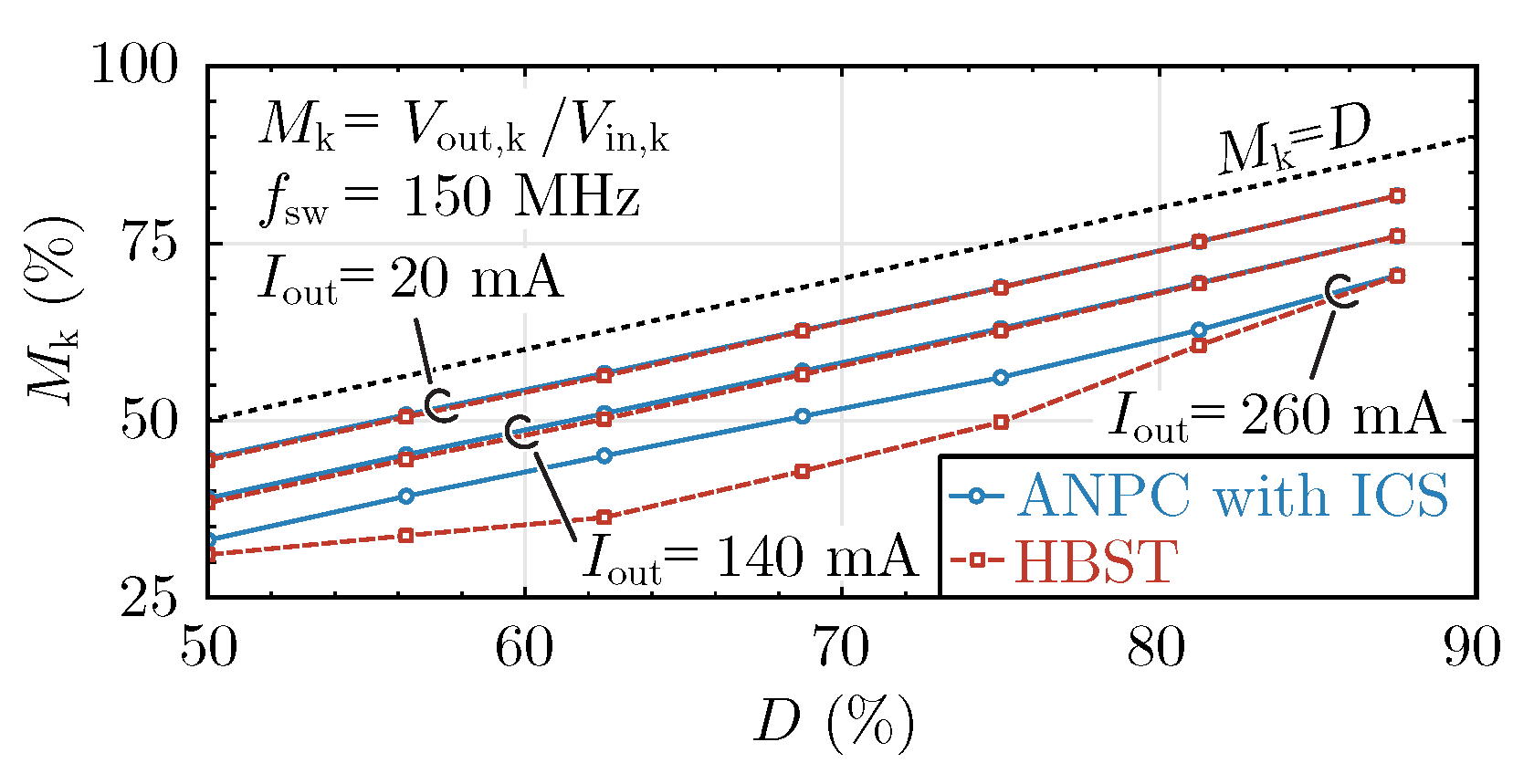
Figure 6. The efficiencies were determined for different dead times during the falling edge of
,
, for the settings listed in
Table 1,
,
,
, and the minimum configurable dead time during the rising edge of
,
, of
, which leads to minimum switching losses during the rising edge of
. As expected, the conventional ANPC HBST featured the best results for very small values of
, due to the additional losses during the dead time, as shown in
Figure 4. The efficiency characteristics of the conventional HBST and the ANPC HBST with ICS were approximately parallel, which was attributed to the similar processes that occur during the corresponding dead times. However, the conventional HBST generated higher losses in
and
than the ANPC HBST with ICS during the rising edge of
; cf.
Figure 3h and
Figure 5j. In summary, the ANPC HBST with ICS achieved the highest efficiency for
overall; for
, the efficiency decreased due to increasing turn-on losses (during
in
Figure 5) and for
due to increased conduction losses during the dead time.
3. Realized IVR
The realized hardware demonstrator was a four-phase IVR, which was comprised of the Power Management IC (PMIC) that was bonded to a PCB.
Figure 7a shows a picture of the hardware demonstrator. The PCB contains the PMIC, four discrete output inductors (one PFL1005-36NMR device, manufactured by Coilcraft, for each converter phase), and additional buffer capacitors. The PMIC contains four power stages, all gate drivers (each gate driver consists of a three-stage gate driver circuit, as explained in [
6]), a high-frequency digital PWM, a configurable load resistor that emulates the power dissipation of a microprocessor, and limited internal buffer capacitances to stabilize the voltages at the input terminal (
) and the mid-point terminal (
), both with respect to the ground.
Figure 7b depicts the chip layout of the power stage of one converter phase. The Front-End-Of-Line (FEOL) area of the HB is 0.0081 mm
. The switching frequency,
, can be adjusted between 50 MHz and 150 MHz. A detailed explanation of the realized demonstrator was given in [
6].
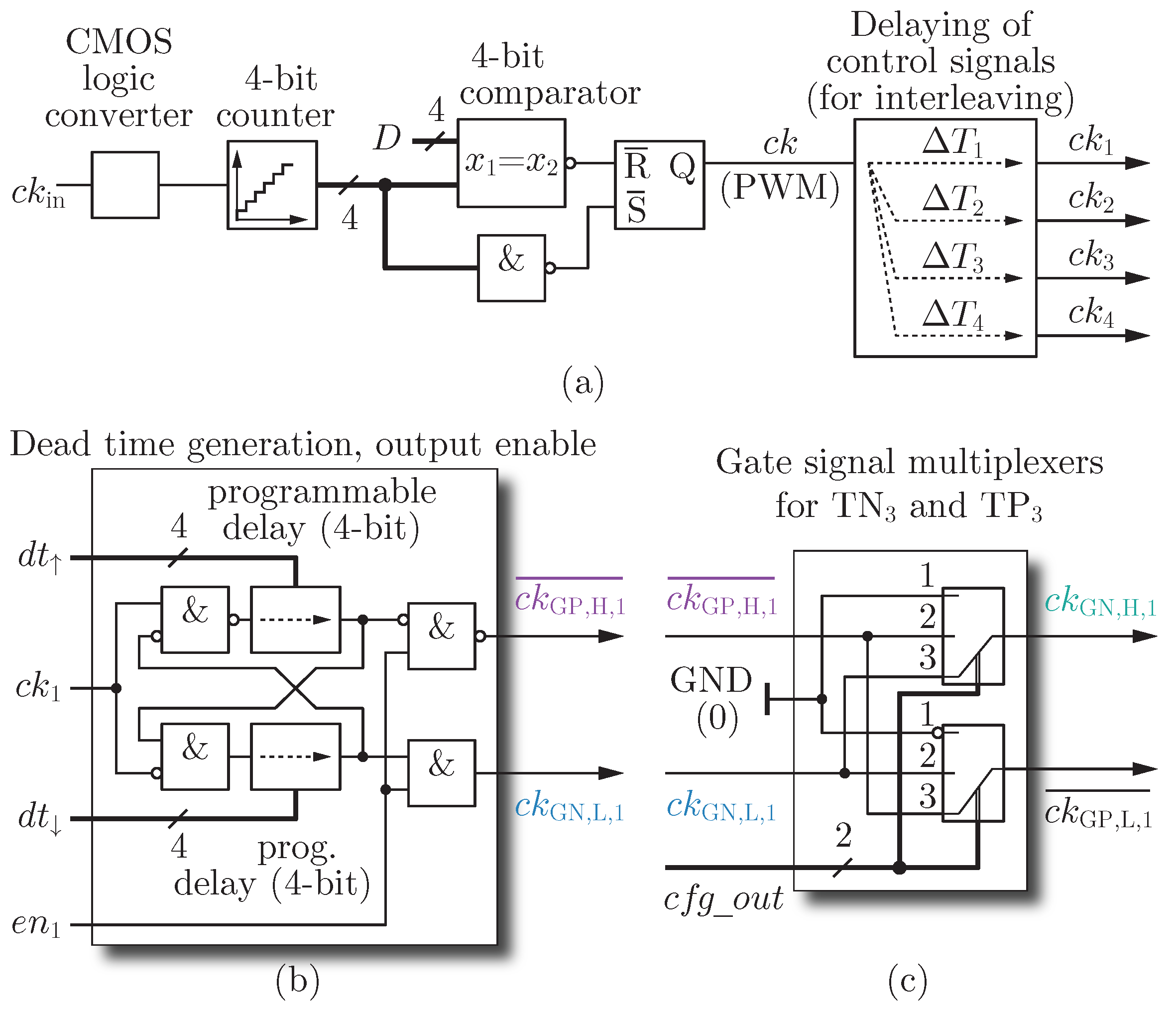
Figure 8 depicts the functional blocks that generate the gate signals for the power transistors, i.e., the digital PWM unit (
Figure 8a), configurable dead time generation units (
Figure 8b), and gate signal multiplexers (
Figure 8c). The circuitries shown in
Figure 8b,c were separately implemented for each converter phase. The PWM unit receives the input clock from the clock signal
and generates a PWM signal,
, that features 16 discrete duty cycles. The output of the PWM unit is connected to the configurable delay block, which realizes the phase-shifted gate signals
, in order to enable interleaving. Each dead time generation unit uses one output signal of the configurable delay block, e.g.,
in the case of Converter Phase 1, to generate the gate signals depicted in
Figure 8a and includes an output enable logic that is controlled by
to allow for the deactivation of selected converter phases (phase shedding). Two four-bit values, which represent
and
, are used to configure the respective dead times. Finally, the multiplexer circuit employs the two-bit configuration signal
to configure how the gate signals for the clamp switches are generated. With this, the three investigated topologies can be emulated: HBST (Position 1), ANPC HBST (Position 2), and ANPC HBST with ICS (Position 3).
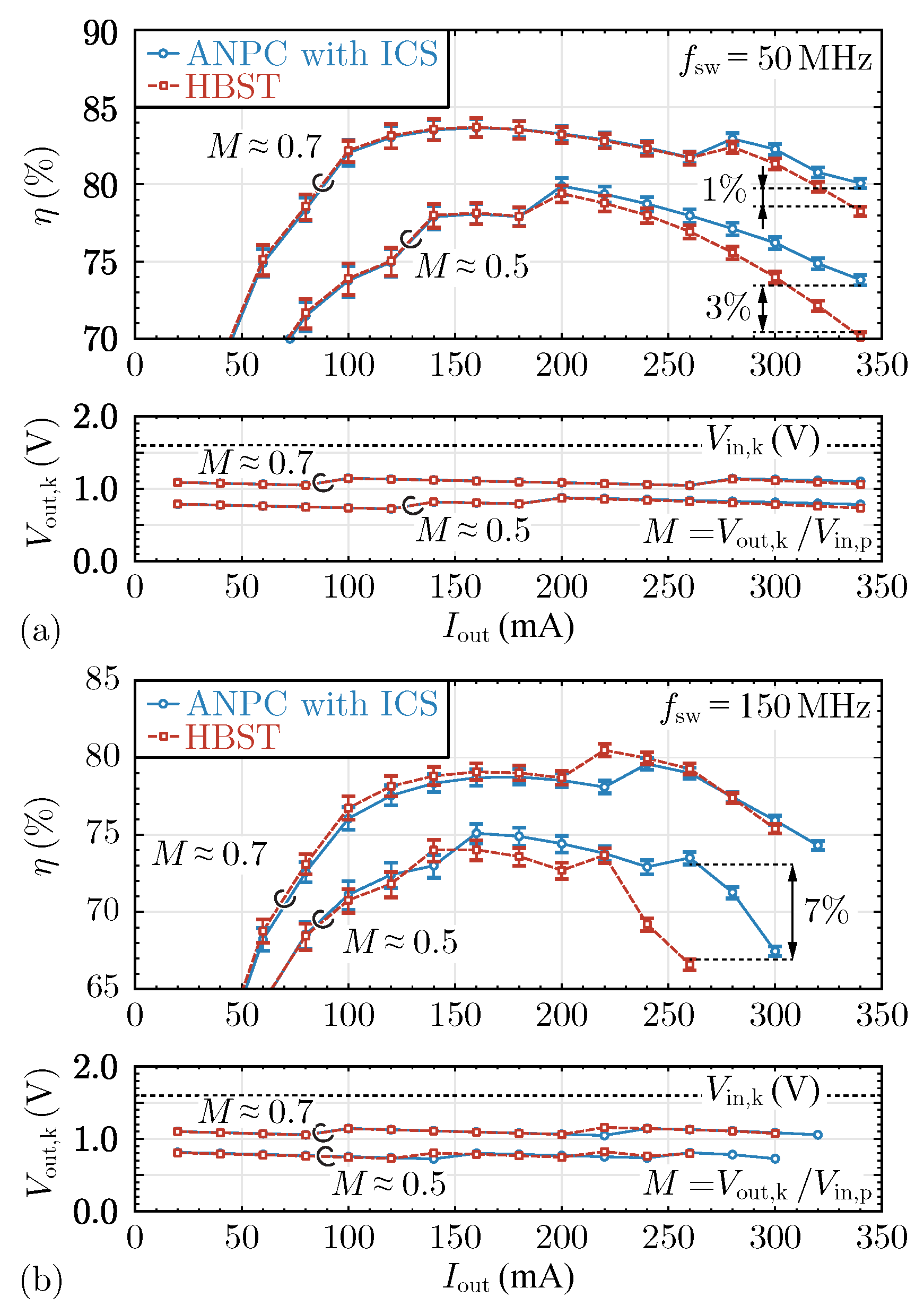
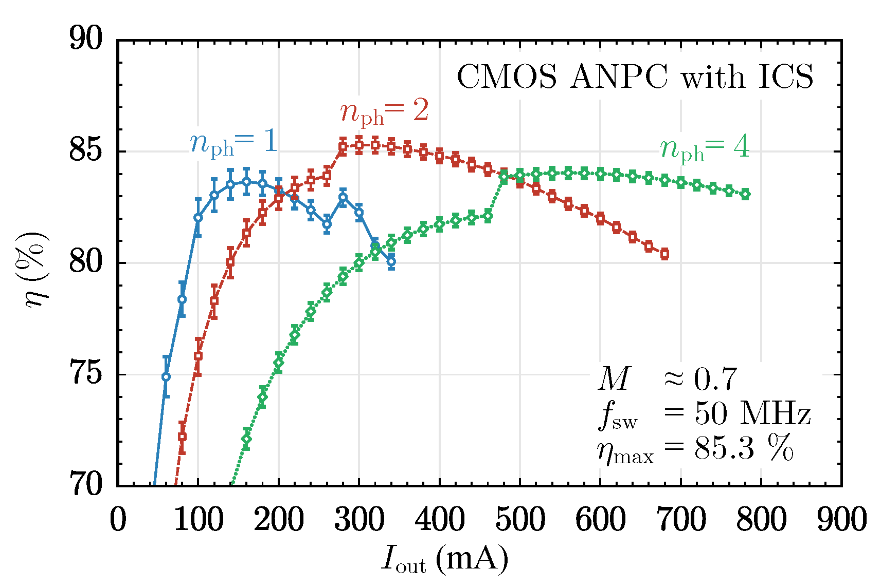
5. Discussion
The footprint area of the Power Management IC (PMIC) of the investigated IVR is comparably small, which enables a very high current density of 24.7 A/mm
. (In this paper, the current density of the PMIC was defined as the maximum output current of the IVR divided by the area of the enabled power switches, gate drivers, and level shifters.) In comparison, the realization presented in [
14], which is also based on a
CMOS technology and operates the buck converter in discontinuous conduction mode, reveals a current density of approximately 10 A/mm
(estimated based on Figure 8.5.7 in [
14]).
The maximum achieved efficiency of
is in a similar range as the efficiencies achieved in [
11,
12,
14] (84% for 1.5 V:1.15 and
in [
11], 80% for 1.2 V:0.93 V and
in [
12], and 88% for 1.6 V:1.2 V and
in [
14]). The decreased efficiency values are due to substantial conduction losses in the thin conductors of the metal layers and the power distribution network of the 14 nm CMOS technology node [
6]. Accordingly, IVRs realized in more mature CMOS technology nodes can achieve higher maximum efficiencies, e.g., in [
25], a peak efficiency of 91.5% was reported for an IVR realized in a 40 nm technology (3.3 V:2.4 V,
). Conversely, the interconnects in CMOS nodes with higher integration levels, e.g., 7 nm, will be even thinner and, thus, more prone to generate even higher conduction losses. For this reason, future research is expected to increasingly address alternative realizations of the IVR’s PMIC that are not directly integrated into the die of the microprocessor, e.g., 3D realizations as presented in [
26].


 ,
, 


