Article

Extending the Input Voltage Range of Solar PV Inverters with Supercapacitor Energy Circulation

1
Department of Electrical and Electronic Engineering, Auckland University of Technology, Auckland 1010, New Zealand
2
Department of Electronic Engineering, School of Engineering, The University of Waikato, Hamilton 3216, New Zealand
*
Author to whom correspondence should be addressed.
Electronics 2021, 10(1), 88; https://doi.org/10.3390/electronics10010088
Submission received: 17 November 2020 / Revised: 14 December 2020 / Accepted: 28 December 2020 / Published: 4 January 2021
(This article belongs to the Section Power Electronics)

Abstract

:
Cleaner and greener energy sources have proliferated on a worldwide basis, creating distributed energy systems. Given the unreliable nature of the renewable sources such as solar and wind, they are traditionally based on inverters interfaced with legacy AC grid systems. While efficiency, output waveform quality and other technical specifications of inverters keep improving gradually, only limited attention is given to widening the input range of inverters. This paper presents a new supercapacitor assisted (SCA) technique to widen the input range of an inverter without modifying the inverter itself. Developing a prototype version of a 24 V DC input capable supercapacitor-assisted wide input (SCASWI) inverter using a supercapacitor circulation front end and a commercial 12 V DC line frequency inverter is detailed in the article, explaining how the SCASWI inverter technique doubles the input voltage while maintaining the useful characteristics of the commercial inverter. The new technique has the added advantage of DC-UPS capability based on a long-life supercapacitor module.

1. Introduction

Minimizing emissions, moving away from fossil fuels, and developing more environment-friendly alternative energy resources have become the modern trend of energy-related research on a worldwide basis. Along with this trend, the distributed generation of clean renewable energy technologies has emerged widely, helping to address geographical and socio-economic challenges in developing countries, considering that around 20% of the world’s population have no access to electricity [1,2]. One of the renewable sources that receives much attention in this context of solving both environmental and accessibility concerns is solar photovoltaic (PV) power. With the steadily increasing penetration of residential and small commercial PV generation, interest has grown in utilizing this renewable generation source to support clean power generation. The output of a solar photovoltaic generator is DC and hence it requires an inverter to interface with the normal AC utility supply in a building or a complex of buildings. The inverter is an essential piece of equipment that converts the direct current (DC) power from the PV array to alternating current (AC) both in grid-connected generation and stand-alone applications [3].
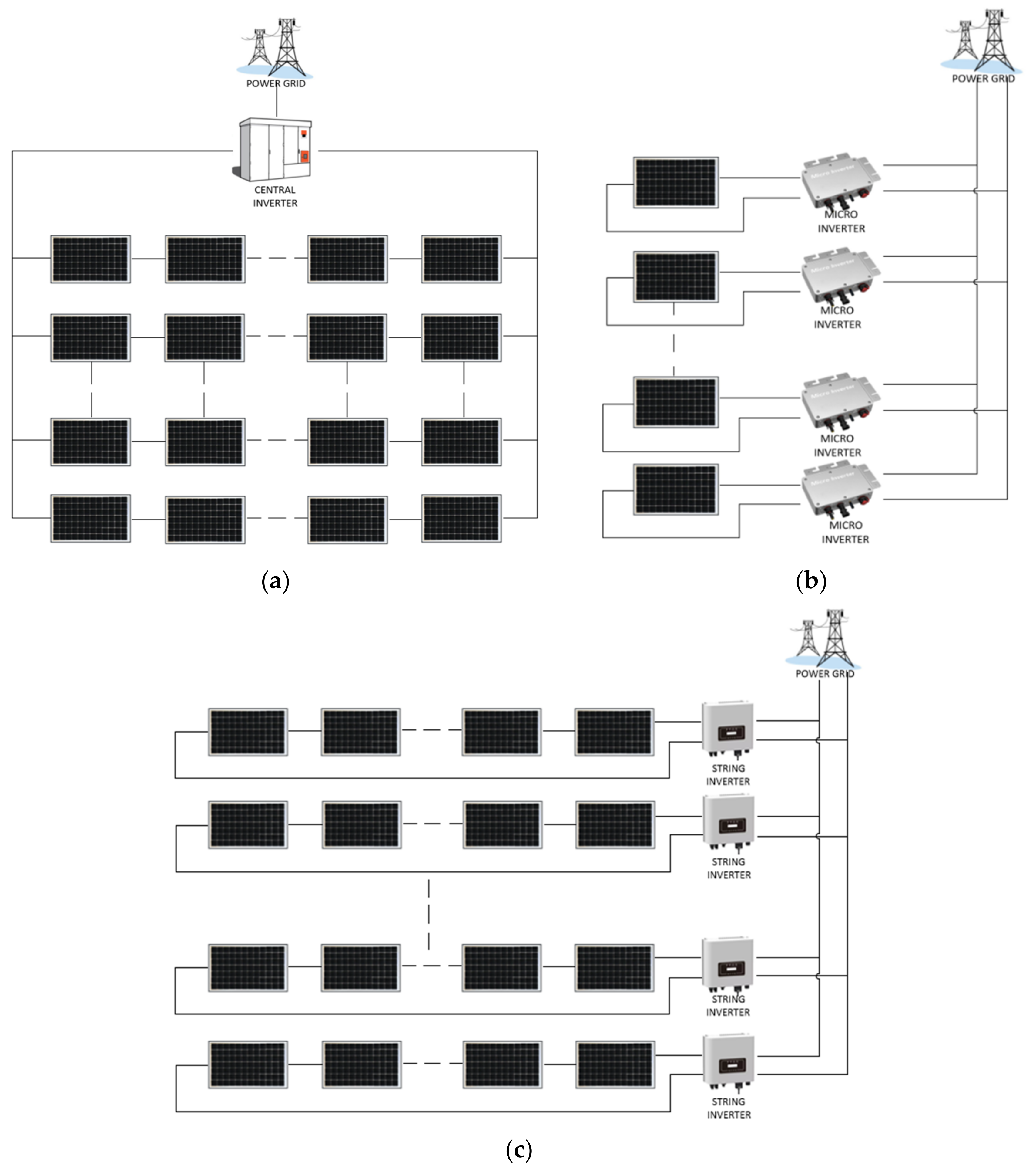
An inverter is a critical component in PV generation and there are different energy extraction characteristics for different inverter configurations. At present, typical inverter configurations used in a solar PV system include central, string and micro inverter-based PV systems. Figure 1 shows the conceptual block diagrams of these three inverter configurations [4].
A central inverter is a high-capacity inverter designed for use with large commercial or utility (power station) sized solar systems as shown in Figure 1a. A string inverter is connected to a series of solar panels and converts the power from DC into AC, for the entire solar system as shown in Figure 1c.
A string inverter will usually be located a short distance away from the PV array in a sheltered location between the solar array and the switchboard. This is the most common type of inverter used in residential and small /medium commercial systems. Micro-inverters are attached to each panel in the solar panel system and DC to AC conversion is done individually as shown in Figure 1b. Micro-inverters best suit partially shaded roofs so that shade affecting one panel will not affect other unshaded panels and is useful on roofs that are too small to enable a string of panels to be installed. Over the past few years, the solar energy has become a feasible solution wherever solar radiation is accessible and the number of residential-scale photovoltaic (PV) generators is rapidly increasing [5,6]. As investment in solar energy rapidly increases worldwide, so does the market share of the various inverter configurations [7].
In the context of current inverter research, improving the efficiency of inverters has received much attention for utilizing all possible extracted solar power generation. Google’s little box challenge in 2014 [8] was a classic example that showed how the interest among power electronics research communities led to thinking outside the box about developing high power density inverters while reducing power losses to increase the efficiency. Nevertheless, only limited attention for such research is reported in the published literature investigating and improving other important characteristics of PV inverters. Currently, individual Micro PV inverter designs are available in specific input ranges such as 12 V, 24 V, and 48 V for various application purposes [9]. There are practical and economic limitations which motivate having a limited input voltage range so as to standardize inverter designs as far as possible.
However, according to the literature, only a limited number of inverter configurations are available having wider input ranges and providing the feasibility of using a single inverter for a wider range of applications [10]. ABSOPULSE Electronics [11] has developed a microprocessor-controlled inverter delivering up to 100 VA sine wave output power which offers a wide operating input range of 20–60 VDC (24 VDC, 36 VDC, and 48 VDC input sources in a single unit). Since such an inverter works on all three input voltages, this also simplifies its use in numerous applications in electrical utilities, power plants, telecomms, and for industrial automation and control. The downside of these inverters is the typical efficiency being in the moderate range around 80% at full load and also, they are comparatively expensive. These research gaps motivated us to extend the supercapacitor assisted loss management (SCALoM) theory [12,13,14], developed by our wider research group in New Zealand to develop this SCAWI-PV inverter technique.
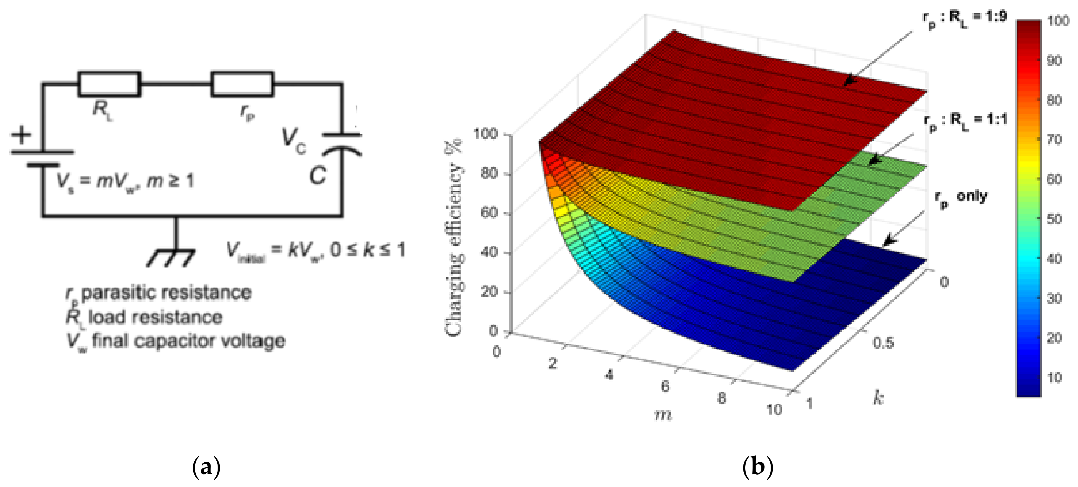
SCALoM theory is an extension of the traditional R-C circuit by (i) adding a power electronics building block (PEBB) into RC the loop, and (ii) replacing the capacitor with a device several orders of magnitude larger. Based on this concept, numerous supercapacitor assisted (SCA) power converter circuit topologies have already been successfully developed over the last 10 years by our two research groups jointly in New Zealand with multiple patents and publications. A few examples are SCA low dropout regulator (SCALDO) [14,15], SCA surge absorber (SCASA) [16], SCA wide input PV inverter (SCAWI-PV Inverter), and SCA light-emitting diodes (SCALED) [17].
In this research, the SCALoM operating principle is applied to the development of a SCAWI-PV inverter. New versions of supercapacitors come in capacitances from 0.2 F to 7500 F but have the limitation of very low DC voltage ratings from 0.7 V to 4 V [18,19,20]. Furthermore, these new developments and the availability of supercapacitors with higher capacitances in a small can size with low ESRs make compact versions of SCA applications a reality [21].
In this paper, the design and development of SCAWI-PV inverter are discussed along with the following structure. Section 2 provides a summary of SCALoM theory. Section 3 provides the conceptual background of the supercapacitor assisted wide input PV inverter (SCAWI-PV inverter) and its operational modes thereby extending the application scope of SCALoM theory. Section 4 illustrates the details of the integration of the DC-UPS capability into the SCAWI-PV inverter. Section 5 shows the prototype implementation of widening the input voltage range of a 12–120 V commercial inverter to be used as 24–120 V inverter with a supercapacitor circulation at the front end and shows the verification of the theoretical claims with the experimental results.

2. Supercapacitor Assisted Loss Management (SCALoM) Theory

The SCALOM theory is an extension of the traditional textbook Resistor-Capacitor (RC) circuit theory in a way to achieve higher charging efficiency in the charging loop using the advantage of a large time constant of a supercapacitor combined with partially charging state along with a useful resistive load in the loop. Starting from the traditional RC theory, the fundamental background of this theory is described in three stages (Section 2.1, Section 2.2 and Section 2.3) as follows:

2.1. Adding a Useful Load into Traditional RC Charging Loop

In a simple RC charging circuit as shown in Figure 2a, an uncharged capacitor starting from a zero-charge achieves an energy content of 1 2   C V S 2 after about 5RC time constants if the input source voltage is VS.
During this time, the resistive components (rp: parasitic circuit resistance) in the loop wastes an equal amount of energy ( E r p ) irrespective of the value of its resistance, so the charging process is 50% efficient. This loss can be written as in Equation (1).
E r p = 1 2 C V 2   ,
The simple RC circuit can be modified as shown in Figure 2b by inserting another resistive load in series with rp as a useful resistive load (RL) which is a power electronics building block (PEEB) such as, a loaded DC-DC converter, a loaded inverter, or any other “useful” resistive load (i.e., a heating element). When the circuit is modified by inserting RL, total loop resistance becomes (rp + RL) and the wasted energy due to rp is negligible if RL >> rp. Therefore, the energy loss due to rp is now reduced as defined in Equation (2).
E r p = 1 2 C V 2 r p r p   +   R L ,
Then, the overall charging efficiency of the system in Figure 2b, can be expressed as:
η = 1     1 2 r p r p   +   R L ×   100 %   ,

2.2. Inserting a Partially Charged Supercapacitor into the Charging Loop

Figure 3 depicts the second modification to the case in Figure 2a by inserting a supercapacitor into the charging loop, with a pre-charge voltage of kVW together with the supply voltage increased to Vs = mVw.
This is to take the advantages of a high charge/discharge capability of supercapacitors as well as the very long-life cycles of commercial supercapacitors (which are several orders larger than rechargeable batteries) [22]. For calculations, k is defined as the pre-charge factor and m is defined as the power supply over-voltage factor [13]. By adding a supercapacitor, which is almost 5–6 orders of a larger capacitance compared to a normal capacitor, the circuit becomes very slow and it allows easier changes from charge to discharge of the capacitor using low cost, low –speed switches.
In the partially charging curve of the SC displayed in Figure 3b, the capacitor voltage (Vc (t)) increases from kVW to VW, during the period t1 to t2, respectively: where k (0 < k ≤ 1) is the initial voltage fraction. The efficiency of the charging under these conditions can be determined as a function of k and m as below.
The increment in stored energy in the supercapacitor ( E C ) between time t1 and t2 is
E C t 1 , t 2 =   1 2 C   V w 2 1 2 C   k V w 2   = 1 2 C   V w 2 1 k 2 ,
The voltage across rp during the SC charging process as per Figure 3a is given in Equation (5).
m V w   V C t = m V w m V w   1   e t r p C   =   m V w e t r p C ,
while the energy loss in r p over t1 and t2 time interval is given by the integral as
E r p t 1 , t 2 =   t 1 t 2 i t 2 × r p × d t ,
where i t 2   r p = m V w     V C t 2 r p   =   m 2 V w 2 e 2 t r p C r p .
Integrating (6), and substituting leads to,
E r p t 1 , t 2 = C V w 2 2 k 2 2 k m + 2 m 1 ,
The charging efficiency (η) of partially charging process of SC from t1 and t2 is given by
η =   E C E r p   +   E C ×   100 % = 1     k 2 2 m 1     k × 100 %   =   1   +   k 2 m × 100 % ,
In the limit k → 0 (with no capacitor precharge) and m → 1 (no power supply overvoltage factor), the efficiency (η) > 1/2, giving the standard textbook result according to Figure 2a. Equation (8) shows that the efficiency is enhanced if the capacitor carries a percentage charge—so it is never allowed to fully discharge during a cycle: thus, avoiding the large energy losses that accrue when current is high. The optimum efficiency is achieved when (k, m) equals to (1:1).

2.3. Combining the Useful Load and the Partially Charged Supercapacitor in the Charging Loop

Figure 4 depicts the overall case with the resistive load, parasitic resistance and the partially charged supercapacitor working in a very long RC time constant circuit.
The charging efficiency defined in Equation (8) can be further improved for the case in Figure 4a as below.
E R L , the energy consumption of R L over t1 and t2 time interval is given by the integral as,
E R L t 1 , t 2 =   t 1 t 2 i t 2 × R L × d t ,
Given the case that the energy stored in SC is to be reused in a discharge operation with the energy source disconnected, efficiency expression of Equation (8) gets modified to
η =   E C     +   E R L E C   +   E R L   +   E r p   ,
After completing similar simplifications steps for Equation (9) as in Equation (7), this modifies the efficiency expression of Equation (10) to
η = 1 1   +   p p + 1 + k 2 m × 100 % ,
where p = R L / r p and p > 1.
The derivations of Equation (11) are given in Ariyarathna et al. [13]. The trends of Equation (11) are illustrated in Figure 4b which shows that when the ratio ( p = R L / r p ) is getting larger, the efficiency advantage increases significantly. The middle and upper traces of Figure 4b depict this claim for rp: RL= 1:1 and 1:9, respectively.
Given the above case of improving the overall charging efficiency of an R-C circuit loop by inserting a useful resistive load, a pre-charged supercapacitor, and an increased power source to suit the overall implementation, loss within the R-C loop can be managed effectively to achieve high- efficiency power converters and protection circuits [22]. This is now introduced as the SCALoM theory, making use of the basis of Equation (11). In a discharging phase of the circuit, based on low-speed switches inserted into the loop as appropriate, the input power source can be disconnected in the discharging phase, maintaining the energy balance of the supercapacitor. SCALDO [14] and SCALED techniques [23] are typical application examples of this SCALoM theory.
Fundamentally this concept is looking at the advantage of replacing the traditional microfarad order capacitor with one million times larger capacitance of a supercapacitor, based on the RC circuit theory extended by appropriate circuit modifications. It is important to note that, the primary use of (an ideal) supercapacitor in all SCALoM theory-based converter applications is equivalent to inserting a lossless voltage dropper element into the charging loop and re-using the excess charge in the load in the second phase of the cycle. The application scope of supercapacitors in SCALoM based non-traditional applications is completely different from traditional energy storage applications of supercapacitors which are complementary to other storage devices such as batteries. Table 1 summaries the comparison of characteristics of supercapacitors versus batteries which supports the selection of supercapacitor as an ideal candidate for developing SCALoM based converter applications due to its very low ESR, high cycle time, power density, and high charge/discharge efficiency.
In the next section, we demonstrate the development of useful application of the aforementioned SCALoM theoretical concept. Section 3 discusses an application of RC loop extension where a partial charging of a supercapacitor occurs with a loaded commercial inverter as the useful load in the charging loop.

3. Extending SCALoM Theory Specifically Towards Developing the Supercapacitor Assisted Wide Input PV Inverter (SCAWI-PV Inverter)

Here, the SCALoM theory discussed in 
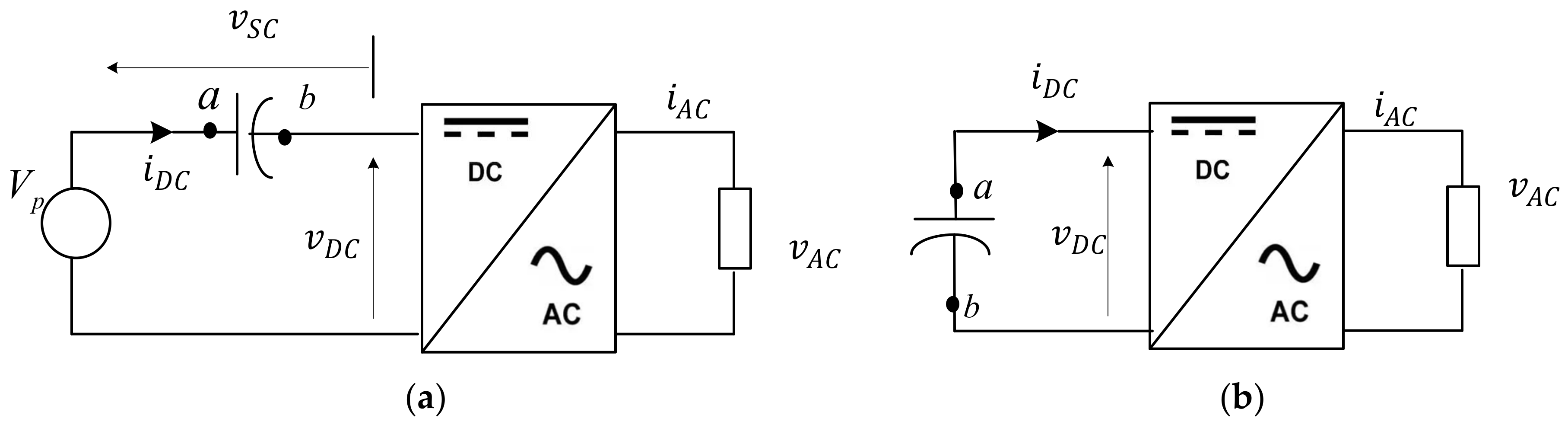
Section 2 is extended for a power electronics application, where the terms in partially charging RC loop is represented as a low voltage input commercial inverter (R) and a supercapacitor (C), as shown in Figure 5a. The theoretical background of utilising the charging efficiency advantage given in Equation (11) is described below for the inverter application.
In this design, a single-phase inverter is chosen with its VA rating such that,
V D C I D C × η i n v e r t e r   = V A C I A C ,
where V D C and I D C are the nominal values of voltage and current of the DC side of the inverter, η i n v e r t e r is the efficiency of the commercial inverter and V A C and I A C are the full load ratings of the AC output characteristics, respectively.
In the proposed inverter configuration shown in Figure 5a and satisfying the conditions of the SCALoM theory, the supercapacitor (SC), with capacitance of C S C , is pre-charged to V D C m i n and placed in series with the commercial inverter connected to an input DC voltage supply of V p in charging arrangement. At an any given time during the SC charging process:
V p =   V D C t + V S C t   ,
where V D C t and V S C t are the instantaneous voltages across the inverter and the SC, respectively. The SC voltage is allowed to charge up from V D C m i n to V D C m a x while the inverter input changes from V D C m a x down to V D C m i n by selecting the DC input supply V p to satisfy the relationship in Equation (14).
V p = V D C m i n + V D C m a x ,
As a result of adding the SC as a voltage dropper in the series path of an inverter, the input DC supply source required to drive the same inverter has changed to the new value V p which is obviously a higher value than the original inverter input voltage, V D C .
Furthermore, the average value of the inverter input is,
V D C a v g = V D C m i n   +   V D C m a x 2 = V p 2 ,
This shows that
V p = 2 V D C a v g ,
For example, if the original commercial inverter input voltage is 12 V, now the overall system is powered by a voltage supply of 24 V. These voltage levels are more commonly used in microinverter designs which use separate inverter modules for different application purposes.
The selection of the SC is based on the required voltage rating of the inverter. SC voltage rating should be greater than V D C m a x . With the limited voltage rating of single SC, the SCs available in the market would be selected to make a compact design by placing the SCs in series to match the required voltage rating.
The amount of energy supplied by the DC source during the charging phase is,
E c h a r g e   = V p i D C a v g t = 2   V D C a v g i D C a v g t ,
where I D C a v g = I D C m i n   +   I D C m a x 2 .
According to Equation (17), the total energy requirement in the charging phase is increased to 2 times the energy required by a single inverter for the charging phase simply because of the fact that the inverter and the supercapacitor both consume and store energy respectively in this phase. The supply should therefore be able to handle this additional energy requirement.
When the threshold condition V D C m i n is met, the charging phase ends, V p supply will be disconnected and the stored energy in the SC will be used to drive the inverter operation during the discharging phase as shown in 
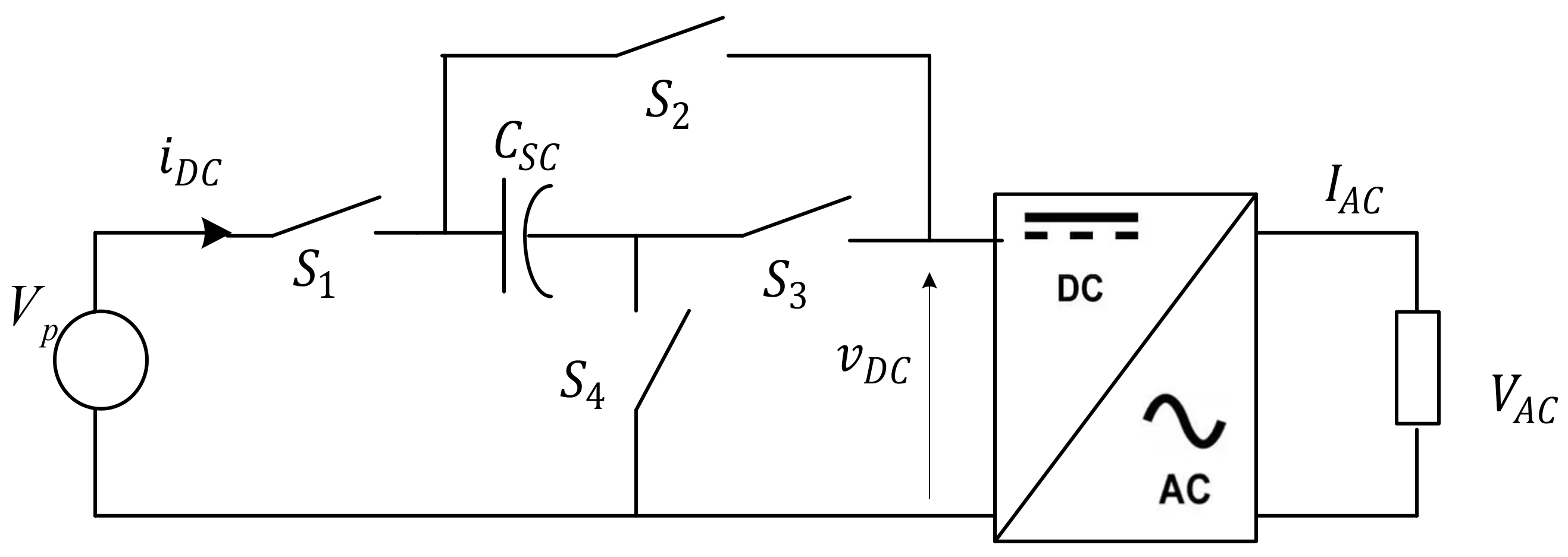
Figure 5b. The switching arrangement of the circuit is shown in Figure 6 and the switching scenarios are given in Table 2.
Energy drawn from the DC source for the inverter operation in the discharging phase is theoretically zero joules.
E d i s c h a r g e   = 0   J ,
P a v g   = 2   V D C a v g i D C a v g t   +   0   ×   t t   +   t = V D C a v g i D C a v g
As shown in Equation (19), the extra energy stored in the charging phase is compensated for in the discharge phase. The SC discharging phase is started with a voltage V D C m a x across the input of the SC and the inverters as shown in Figure 5b. The SC discharging process will be continued until the supercapacitor voltage reaches the minimum working input voltage of the inverter   V D C m i n . Then, the switching network will be activated again, and the circuit operation will be placed back into SC charging phase as shown in Figure 5a. This process will be continued cyclically.
Throughout the charging and discharging cycles, the SCASWI-PV inverter is in continuous operation and the efficiency ( η S C A ) in an ideal situation can be expressed as follows:
η S C A =   V A C I A C           V D C a v g   I D C a v g ,
The above efficiency figure in Equation (20) is close to the commercial inverter’s ideal efficiency as denoted in Equation (12), which can be rearranged as to show the original inverter’s efficiency as,
η i n v e r t e r =   V A C I A C           V D C I D C ,
Although the input voltage range of the inverter has been extended to a new value as per Equation (14) in the SCASWI-PV inverter, it can still maintain an efficiency very much closer to that of the original inverter. This effect removes the downside of using another new inverter for a higher input voltage application. The input voltage range can be further widened using a SC matrix and switching it in a switched-capacitor arrangement to achieve different types of voltage requirements of inverters. This arrangement is beyond the scope of this paper.
The above-mentioned inverter range extension scenario is applicable for any type of DC input and any inverter topology. It does not necessarily need to be a PV input to the inverter. However, in this paper, we primarily look at applying the scenario of microinverter design which is commonly used with PV inputs.

4. Integration of DC-UPS Capability

In the previous discussion, the selection of SCs was primarily limited to design a compact prototype. The major design constraint was to minimize the number of SCs to match the voltage ratings of the inverter while effectively choosing a low-cost SC to handle the maximum load current capability of the input side. The availability of SCs with larger capacitances in the range of a few thousand Farads in a single cell (e.g., 3,000 F) gives the design flexibility to select a relatively oversized SC as the series dropper element. This choice will not make the design excessively bulky as the SCs are a small physical size considering the million times larger capacitance they provide. By selecting an oversized SC with its new capacitance C S C o v e r s i z e , this capacitor can be used as an extra-energy-buffer to safeguard against short-term disruptions to the input DC power supply.
In this UPS capability integration approach, the minimum working voltage of the inverter is modified to a new value ( V D C U P S ) which is a slightly higher value than the previously selected   V D C m i n of the inverter. During normal operation, in the modified UPS enabled topology, the series SC charges until the inverter DC input voltage ( V D C t ) reaches,   V D C U P S . Then the inverter operation switches to the discharging mode where the SC takes the time to discharge until the UPS input voltage drops back to V D C U P S .
In a DC input power supply disruption during the charging phase of the SC, and if the input voltage of the UPS is disrupted at V p d i s t r u p t , then the voltage across the C S C o v e r s i z e , is reached and the amount of energy stored corresponds to the rise of change of ( V p - V p d i s t r u p t ) at that point. The stored energy in the oversized SC at this moment is substantially large, and it can be used to continue the UPS operation until the UPS input voltage drops back to V D C m i n for a significant time. By introducing an oversized SC and changing the minimum working voltage of the inverter to a slightly higher value, the DC-UPS feature can be integrated into the SCAWI-PV inverter design without using any additional hardware. Even if there is a disruption of DC power supply during the normal discharging operation of the new topology, the discharging mode can be further continued to until the inverter input voltage drops to its real minimum working voltage V D C m i n . An example of this DC UPS capability will be demonstrated with experimental results in the next section.

5. Experimental Validation

5.1. 24VDC-120VAC SCAWI-PV Inverter Prototype Implementation
With the use of a 12 VDC–120 VAC/50 Hz commercial sinewave inverter (Mdaoud Electrical Ltd, Shanghai, China), the SCAWI-PV inverter prototype was implemented to extend the input voltage of the inverter to 24 VDC. The input voltage range of the inverter is specified as 11–13 VDC by the manufacturer. Therefore, V D C m i n was maintained at 11 V. The selected SC bank (VInaTech VEM16R0606QG, Ropla Elektronik., Suchy Dwór, Poland) at the front end of the inverter for energy circulation is rated at 60 F with a maximum operating voltage of 16 V. The low-frequency SC energy recovery method was managed by five low-speed MOSFET switches as depicted in Figure 7a.
IPP120P04P4L-03 P-channel MOSFETs (VDS = 40 V, RDS(on) = 3.1 mΩ, ID = 120 A) were used for the S1, S2 and S3 switches. For S4 and S5, IRF740 N-channel MOSFETs (VDS = 400 V, RDS(on) = 0.55 Ω, ID = 10 A) were used. Switches S1 and S3 control supercapacitor charging, while S2 and S4 control the discharge phase. During the off state of S3, the body diode of a single MOSFET is forward biased with the SC bank voltage and this causes problems for proper operation. To eliminate this problem, S3 was made up of two back-to-back P-channel MOSFETs. At the initial startup of the circuit, to bring the SC bank voltage close to V D C m i n , an additional switch (S5) along with a series charging resistor (Rc) was used. The source voltage was kept fixed at 24V during the testing.
The switches were optically isolated and were controlled by digital outputs of an ATMEGA328P based embedded system. This controller continuously monitored the input voltage of the inverter and the voltage across the SC bank via its analogue inputs. The switching algorithm of the MCU satisfied that the inverter was operated within its rated input voltage range and the SC bank was charged below its maximum voltage. To keep the inverter powered during switching transitions, a buffer capacitor (1 mF/35 V) was connected across the input terminals of the inverter. The experimental setup of the prototype is shown in Figure 7b.

5.2. Steady-State Operation

The steady-state performance characteristics of the 24 VDC–120 VAC SCAWI-PV inverter was compared against the performance of the standalone 12 VDC–120 VAC inverter. Figure 8 shows the input/output voltage waveforms of the commercial inverter when running at 100 W output load before the SCAWI technique is applied.
Figure 9 depicts the input/output voltages of the SCAWI-PV inverter when the output was set to 100 W. As can be seen from these oscilloscope traces, the input voltage of the inverter varies between 11 V and 13 V with a very low switching frequency (<1 Hz) while the output is fixed at 120 V/50 Hz. The low-frequency ripple amplitude is very low compared to the fundamental 50 Hz component, and it can be further reduced by keeping the input voltage variation at a minimum level.

5.3. Power Losses and End-to-End Efficiency

The primary losses of the SCAWI-PV inverter are similar to the losses associated with primary SC-assisted topology [24]. These key implementation losses are estimated based on the maximum output power and the rated expanded voltage (24 V) and listed in Table 3.
This estimation is based on manufacturers’ specifications (for inverter block efficiency) and some operating conditions (e.g.: voltages /currents/capacitor size for switching losses and controller efficiency). The estimated total power loss is about 13 W when the above factors are concerned. The SCAWI-PV inverter prototype had approximately 87% efficiency at 24 V and 100 W output power for the worst-case scenario.
The chosen commercial inverter has an efficiency of 88%. As per Equation (20) and Equation (21), theoretically, in an ideal situation, the SCASWI PV inverter should have the same efficiency as the commercial inverter.
The efficiency of the SCAWI-PV inverter was compared with the standalone inverter for different levels of input power based on the experimental prototype design and the results tabulated in Table 4. The efficiencies are displayed in Figure 10.
This shows that the practical efficiency of the commercial inverter in use has an efficiency in the range from 83% to 89% for 25 W to 100 W input power, respectively. Conversely, when the SC energy circulation front approach (SCASWI design) is applied, the efficiency range margin has changed from 82% to 88% for 25 W to 100 W. This clearly verifies the theoretical claims given in Equation (20) and Equation (21). There is only a 1% loss increase for 25–100 W power range while gaining a wide input voltage range and added DC-UPS capability in the SCAWI-PV prototype. The efficiency of this technique can be maintained very much closer to the efficiency of the standalone inverter by reducing the major loss factors using SCs with low ESR, switches with low RDS(on) resistance and reducing the power consumption of control circuit with discrete low-quiescent current logic gates instead of an MCU.
The design of high input inverters requires MOSFET switches with higher voltage capability for input side switching, which have higher RDS(on) resistances. As a result, high input designs have high losses and low efficiency. On the other hand, in an inverter designed for low input voltage, input side switching transistors are generally low on-resistance MOSFETS, contributing to better efficiency. The 12 V input commercial inverter that was used for the SCASWI design is compared with 24 V input inverter from the same manufacturer as shown in Table 5.
The efficiency numbers clearly show the claimed lower efficiency for the high input inverter and its higher cost. Our technique described here is just an input range extender, without any modifications required within the inverter. All that we added is a set of 4 low-frequency switches with an affordable cost supercapacitor to achieve an inverter with twice the input range while maintaining efficiency closer to low input commercial inverter and having the added advantage of short-term energy buffer based on a long-life energy storage device. Instead of buying a new inverter with high input voltage for different applications, using a low voltage input commercial inverter and SC range extender gives the option to use one inverter and get a higher voltage input with advantages of lowest cost and high efficiency. The entire range extender circuit design cost is much cheaper than buying separate inverters for high voltage input application. The cost of building the prototype version of SC range extender circuitry was around NZD 70.

5.4. DC-UPS Integrated Operation

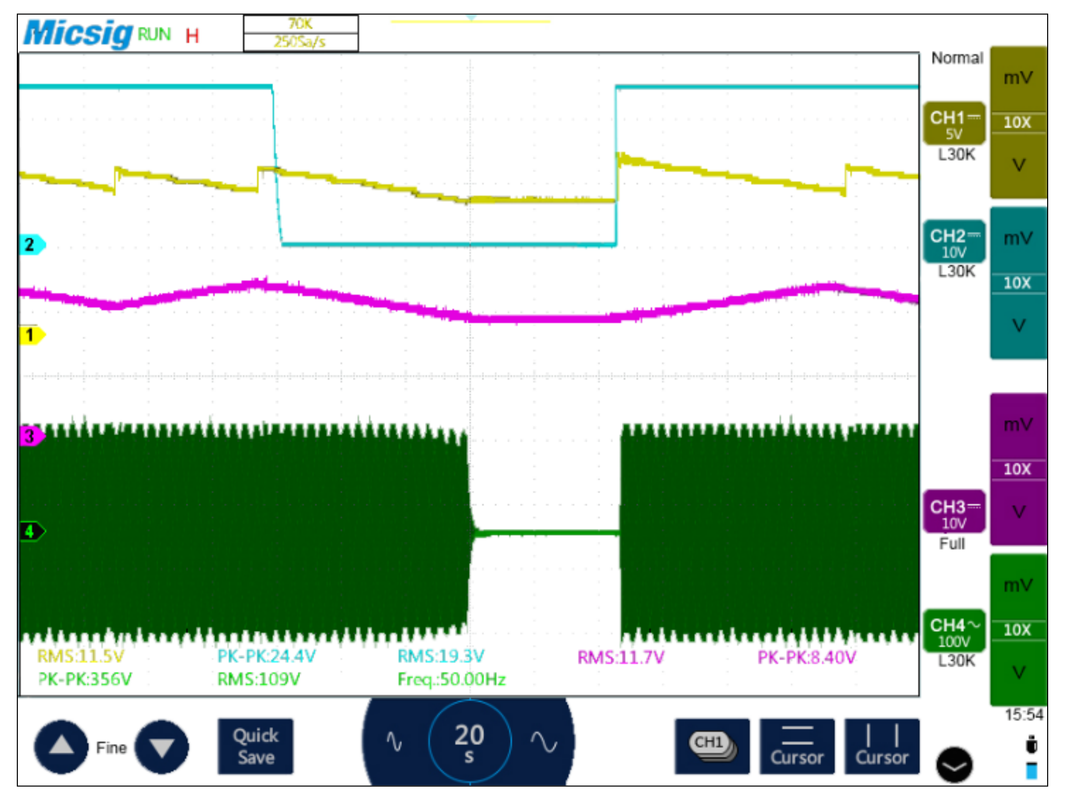
One of the advantages of SCAWI-PV inverter is its DC-UPS capability. When the input supply is disconnected, the stored energy in the SC is used to power the inverter during this period. Figure 11 displays a line interrupt event and how the SCAWI-PV inverter operates during this period. The V D C U P S was selected as 11.5 V, which is slightly higher than the minimum working voltage 11 V (   V D C m i n ) of the inverter in use.
As can be seen from Figure 11, the line interruption occurred during the discharge mode of the SC and its current mode was continued until the input voltage of the inverter diminished to 11 V. The stored energy of the SC was sufficient to keep the inverter running for at least 64 s. The time duration of DC-UPS in operation depends on the capacitance of the SC bank, the efficiency of the system and the output load. Since the input voltage source was not restored after the 64 s and the inverter voltage dropped to   V D C m i n , the inverter was shut down and the SC voltage remains constant. This operation can be seen from the capacitor voltage waveform in Figure 11 as it became a flat line during this deadtime of operation. When the DC source was connected back, the SC was switched to the charging mode and the inverter operation was begun. The deadtime of inverter output voltage during the line disruption can be minimized by increasing the capacitance of the SC bank.

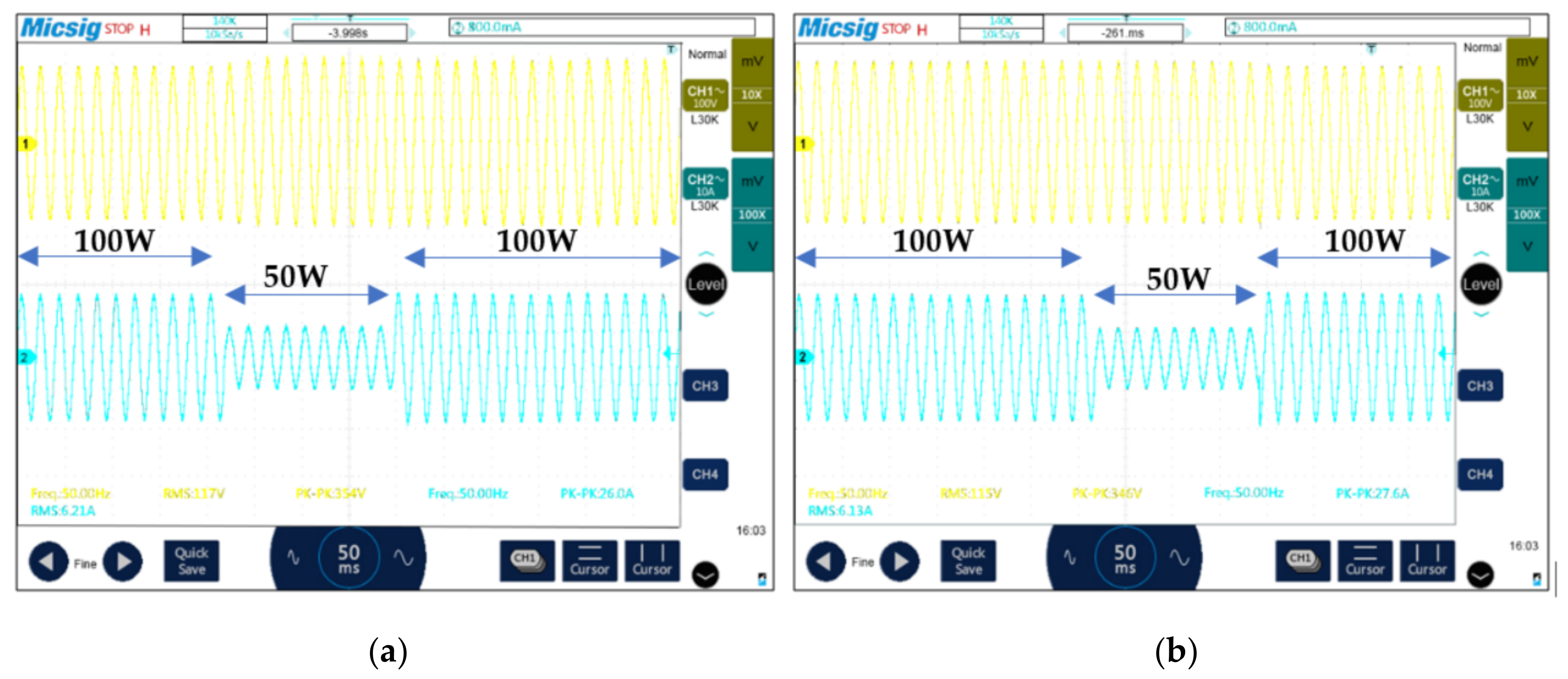
5.5. Load Transient Response

A step load was applied to the PV inverter before and after applying the SCAWI-PV technique and the corresponding output voltage response is displayed in Figure 12. These results imply that the inverter output transient characteristics are not affected even though the case of a SC switching configuration is used for energy recovery and voltage extension at the front end.

6. Conclusions

The SCALoM theory has been successfully applied in the SCASWI inverter design using a commercial inverter as the PEBB in the RC loop and replacing the capacitor with a several orders of magnitude larger capacitor (supercapacitor) to achieve a versatile inverter design to extend the input range of a commercial inverter. In this proof-of-concept project, without doing any modification to the internal circuits of a commercial off-the-self inverter, we have shown that a supercapacitor module can be used to double the input range, without significant deterioration of the efficiency and with no adverse transient effects. The SCASWI PV-inverter design maintains an efficiency range very much closer to the commercial inverter independent from the change made to the input voltage. The 12V–240 V, 100 W commercial inverter has an efficiency range from 83% to 88% whereas SCASWI-PV inverter efficiency ranges from 82% to 87% for the same loads. The 1% discrepancy is due to the losses in the resistive elements in the supercapacitor front end. This technique has the added advantage of a supercapacitor-based energy buffer (DC-UPS capability) for the inverter to overcome any negative effects of solar/ wind type input fluctuations. More elaborate applications of the same design approach using SCALoM theory are in progress into the area of microinverter research.

Author Contributions

Conceptualization, K.G. and N.K.; methodology, K.G. and K.S.; validation, N.B. and K.S.; formal analysis, K.G. and K.S.; data curation, N.B. and K.S.; writing—original draft preparation, K.G., K.S. and N.B.; writing—review and editing, K.G., K.S. and N.K.; supervision, K.G., K.S. and N.K. All authors have read and agreed to the published version of the manuscript.

Funding

This research was funded by Auckland University of Technology.

Institutional Review Board Statement

Not applicable.

Informed Consent Statement

Not applicable.

Data Availability Statement

Not applicable.

Conflicts of Interest

The authors declare no conflict of interest.

References

  1. Al-Hallaj, S. More than enviro-friendly: Renewable energy is also good for the bottom line. IEEE Power Energy Mag. 2004, 2, 16–22. [Google Scholar] [CrossRef]
  2. Veilleux, G.; Potisat, T.; Pezim, D.; Ribback, C.; Ling, J.; Krysztofiński, A.; Ahmed, A.; Papenheim, J.; Pineda, A.M.; Sembian, S.; et al. Techno-economic analysis of microgrid projects for rural electrification: A systematic approach to the redesign of Koh Jik off-grid case study. Energy Sustain. Dev. 2020, 54, 1–13. [Google Scholar] [CrossRef]
  3. Wai, R.; Lin, C.; Huang, Y.; Chang, Y. Design of High-Performance Stand-Alone and Grid-Connected Inverter for Distributed Generation Applications. IEEE Trans. Ind. Electron. 2013, 60, 1542–1555. [Google Scholar] [CrossRef]
  4. Zheng, H.; Li, S.; Challoo, R.; Proano, J. Shading and bypass diode impacts to energy extraction of PV arrays under different converter configurations. Renew. Energy 2014, 68, 58–66. [Google Scholar] [CrossRef]
  5. Silva, M.; Castro, R.; Batalha, M. Technical and Economic Optimal Solutions for Utility-Scale Solar Photovoltaic Parks. Electronics 2020, 9, 400. [Google Scholar] [CrossRef] [Green Version]
  6. Nassif, A.B.; Dong, M. Characterizing the Effect of Conservation Voltage Reduction on the Hosting Capacity of Inverter-Based Distributed Energy Resources. Electronics 2020, 9, 1517. [Google Scholar] [CrossRef]
  7. FUTURE OF SOLAR PHOTOVOLTAIC Deployment, Investment, Technology, Grid Integration and Socio-Economic Aspects. Available online: https://www.irena.org/publications/2019/Nov/Future-of-Solar-Photovoltaic (accessed on 9 November 2020).
  8. Little Box Challenge. Available online: https://en.wikipedia.org/wiki/Little_Box_Challenge (accessed on 9 November 2020).
  9. Ankit; Sahoo, S.K.; Sukchai, S.; Yanine, F.F. Review and comparative study of single-stage inverters for a PV system. Renew. Sustain. Energy Rev. 2018, 91, 962–986. [Google Scholar] [CrossRef]
  10. Caisheng, W.; Hashem, N. Power management of a stand-alone wind/photovoltaic/fuel-cell energy system. In Proceedings of the 2008 IEEE Power and Energy Society General Meeting—Conversion and Delivery of Electrical Energy in the 21st Century, Pittsburgh, PA, USA, 20–24 July 2008; p. 1. [Google Scholar]
  11. RSI 100-D1 Railway DC-AC Sine Wave Inverters. Available online: https://absopulse.com/wp-content/uploads/2019/05/RSI-100-IP66-D1-waterproof-railway-sine-wave-inverters.pdf (accessed on 7 November 2020).
  12. Kankanamge, K.; Kularatna, N. Improving the End-to-End Efficiency of DC–DC Converters Based on a Supercapacitor-Assisted Low-Dropout Regulator Technique. IEEE Trans. Ind. Electron. 2014, 61, 223–230. [Google Scholar] [CrossRef]
  13. Ariyarathna, T.; Jayananda, D.; Kularatna, N.; Steyn-Ross, D.A. Potential of supercapacitors in novel power converters as semi-ideal lossless voltage droppers. In Proceedings of the IECON 2017—43rd Annual Conference of the IEEE Industrial Electronics Society, Beijing, China, 29 October–1 November 2017; pp. 1429–1434. [Google Scholar]
  14. Gunawardane, K.; Kularatna, N. Supercapacitor-assisted low dropout regulator technique: A new design approach to achieve high-efficiency linear DC–DC converters. IET Power Electron. 2018, 11, 229–238. [Google Scholar] [CrossRef]
  15. Kularatna, N.; Fernando, L.J. High current voltage regulator. US7907430 B2, 15 March 2011. [Google Scholar]
  16. Fernando, J.; Kularatna, N.; Round, H.; Tálele, S. Implementation of the supercapacitor-assisted surge absorber (SCASA) technique in a practical surge protector. In Proceedings of the IECON 2014—40th Annual Conference of the IEEE Industrial Electronics Society, Dallas, TX, USA, 29 October–1 November 2014; pp. 5191–5195. [Google Scholar]
  17. Jayananda, D.; Kularatna, N.; Steyn-Ross, D.A. Performance Characteristics of Energy-Efficient LED Lamps Leading to Supercapacitor Assisted LED (SCALED) Technique for DC-Microgrid Applications. In Proceedings of the 2019 IEEE International Conference on Industrial Technology (ICIT), Melbourne, Australia, 13–15 February 2019; pp. 515–520. [Google Scholar]
  18. Yang, H. Estimation of Supercapacitor Charge Capacity Bounds Considering Charge Redistribution. IEEE Trans. Power Electron. 2018, 33, 6980–6993. [Google Scholar] [CrossRef] [PubMed]
  19. Yang, H. Peukert’s Law for Supercapacitors With Constant Power Loads: Applicability and Application. IEEE Trans. Ind. Appl. 2019, 55, 4064–4072. [Google Scholar] [CrossRef] [PubMed]
  20. Sengupta, A.S.; Satpathy, S.; Mohanty, S.P.; Baral, D.; Bhattacharyya, B.K. Supercapacitors Outperform Conventional Batteries. IEEE Consum. Electron. Mag. 2018, 7, 50–53. [Google Scholar] [CrossRef]
  21. Kularatna, N. Supercapacitor Assisted Low Dropout Regulators (SCALDO) for high efficiency DC-DC converters for DC microgrid applications. In Proceedings of the 2015 IEEE First International Conference on DC Microgrids (ICDCM), Atlanta, GA, USA, 7–10 June 2015; pp. 333–338. [Google Scholar]
  22. Kularatna, N.; Jayananda, D. Supercapacitor-Based Long Time-Constant Circuits: A Unique Design Opportunity for New Power Electronic Circuit Topologies. IEEE Ind. Electron. Mag. 2020, 14, 40–56. [Google Scholar] [CrossRef]
  23. Jayananda, D.; Kularatna, N.; Steyn-Ross, D.A. Supercapacitor-assisted LED (SCALED) technique for renewable energy systems: A very low frequency design approach with short-term DC-UPS capability eliminating battery banks. IET Renew. Power Gener. 2020, 14, 1559–1570. [Google Scholar] [CrossRef]
  24. Gunawardane, K.; Kularatna, N.; Steyn-Ross, D.A. Loss estimation and validation of the SCALDO implementation. In Proceedings of the 2015 IEEE 11th International Conference on Power Electronics and Drive Systems, Sydney, Australia, 9–12 June 2015; pp. 89–92. [Google Scholar]
  25. Subasinghage, K. Advanced Analysis of Supercapacitor-Assisted Low-Dropout (SCALDO) Regulator. Ph.D. Thesis, Auckland University of Technology, Auckland, New Zealand, 2019. [Google Scholar]
  26. Gunawardane, K.K. Analysis on Supercapacitor Assisted Low Dropout (SCALDO) regulators. Ph.D. Thesis, University of Waikato, Hamilton, New Zealand, 2014. [Google Scholar]
Figure 1. Configurations of PV system: (a) Centralised system; (b) Detached microinverter system; (c) String system [4].
Electronics 10 00088 g001
Figure 2. R-C circuit leading into SCA techniques: (a) The basic RC circuit, (b) RC circuit and added useful resistance RL.
Electronics 10 00088 g002
Figure 3. Modified Figure 2a by inserting a pre-charged supercapacitor: (a) longer time constant R-C circuit achieved by inserting a supercapacitor; (b) charging curve of the supercapacitor from pre-charge voltage (kVW) to working voltage (VW) which is below power supply voltage mVW.
Electronics 10 00088 g003
Figure 4. Insertion of a useful resistive load into the partially charging RC loop: (a) modified circuit with useful resistance RL (b) Graphical representation of the circuit behaviour in terms of efficiency versus variables m and k.
Electronics 10 00088 g004
Figure 5. The basic circuit diagram of the SCAWI-PV inverter: (a) SC charging phase; (b) SC discharging phase.
Electronics 10 00088 g005
Figure 6. The switching arrangement of the SCAWI-PV inverter.
Electronics 10 00088 g006
Figure 7. 24V-to-120V SCAWI-PV inverter prototype: (a) Informative schematic; (b) Test setup.
Electronics 10 00088 g007
Figure 8. The input/output waveforms of the commercial 12 VDC–120 VAC inverter when the output was set to 100W: Yellow—Input supply voltage, Blue—Input current, Green—Output current, Purple—Output AC voltage).
Electronics 10 00088 g008
Figure 9. The input/output waveforms of the SCAWI-PV inverter operating at 100W output load (Yellow—Input DC voltage, Blue—Input current, Purple—Output AC voltage, Green—Output current): (a) For waveform—duration =5 s; (b) For waveform duration =10 ms.
Electronics 10 00088 g009
Figure 10. Comparison of end-to-end efficiency of the SCAWI-PV technique and the standalone 12VDC-120VAC inverter.
Electronics 10 00088 g010
Figure 11. The operation of SCAWI-PV inverter during a line disruption (Yellow—input voltage of the inverter, Blue—12 V input source voltage, Purple—Voltage across the supercapacitor bank, Green—Output voltage of the inverter).
Electronics 10 00088 g011
Figure 12. Load-Transient response for 100 W to 50 W step load change (Yellow—Output AC voltage, Blue—Output current): (a) Standalone 12 V–120 V inverter; (b) After applying the SCAWI-PV technique.
Electronics 10 00088 g012
Table 1. Comparison of characteristics of supercapacitors versus batteries which supports the selection of supercapacitors in SCALoM-based converter applications.
CharacteristicsSupercapacitorsBatteries
Power density (W/kg)10,00050–200
Energy density (Wh/kg)1–2020–100
Charge/Discharge≈100 %Less than 85 %
Equivalent series resistanceTypically, in mΩ rangeFractional Ω to few Ω
Cycle time50,000–1,000,000500–2000
Charge time1–60 s3600–18,000 s
Discharge time0.1–30 min10–180 min
Table 2. Switching sequence of the SCAWI-PV inverter.
SwitchSC Charging PhaseSC Discharging Phase
S1ONOFF
S2OFFON
S3ONOFF
S4OFFON
Table 3. Estimated power losses in the 24VDC-120VAC SCAWI-PV inverter.
Loss FactorDescriptionEstimated Value
1Ohmic losses due to the ESR of the SC and the switches for 100 W load [25]700 mW
2Dynamic losses during switching [26]≈0 W
3The power consumption of the control unit300 mW
4Energy loss due to the paralleling of capacitors with different voltages [25,26]2 mW
5Power losses in the standalone inverter at 12 V input and for a 100 W load12 W
Table 4. End-to-End Efficiency of the SCAWI-PV technique compared to the standalone 12 VDC–120 VAC inverter.
Output Load Resistance (Ω)Standalone InverterSCAWI- PV Inverter
Input Power (W)Output Power (W)Efficiency (%)Input Power- SC Charging (W)Output Power - SC Charging (W)Input Power-SC Discharging (W)Output Power- SC Discharging (W)Average Efficiency (%)
144113.04100.8089.17114.11100.30104.8892.8088.19
160103.8092.4089.02102.9088.92105.8493.6087.43
180103.5692.4089.2292.2883.30100.7584.4987.07
20682.4473.8189.5382.6071.4084.4272.5986.21
24070.6861.7187.3174.9367.7675.8961.7185.87
28860.1251.1885.1362.4054.4565.5253.2484.26
36050.4041.1481.6350.3942.7051.5342.7083.80
48034.0829.6586.9944.6037.8245.2336.6082.85
72024.7320.5383.0232.2426.1830.2424.9981.92
Table 5. Comparison between 12 VDC–120 VAC Inverter, 24 VDC–120 VAC Inverter and 24 VDC–120 VAC SCASWI Inverter.
ModelMandaou TEP-300-121Mandaou TEP-300-241SCAWI 24VDC-120VAC Inverter
Rated Power300 W300 W300 W
DC input voltage12 V24 V24 V
AC output voltage120 V120 V120 V
No-load current0.5 A0.25 A0.5 A
AC output frequency50 Hz/60 Hz50 Hz/60 Hz50 Hz/60 Hz
AC output waveformPure SinePure SinePure Sine
Efficiency>88%>86%>87%
Unit Price NZD150NZD185Unit price of inverter + NZD 70 (Approximate cost of range extender)
Publisher’s Note: MDPI stays neutral with regard to jurisdictional claims in published maps and institutional affiliations.

