1. The Movement towards Programmable Analog Synthesis
The current lack of available analog synthesis tools makes constructing programmable analog systems, particularly energy-efficient analog and mixed-signal computing systems, significantly more difficult than digital systems. Analog computing typically is more energy efficient than digital computing, starting from Mead’s Hypothesis (1990) [
1] and its experimental verification (2004) [
2]. Analog computation and system designs (e.g., [
3,
4,
5]) demonstrate improved energy efficiency (>
) and area efficiency (>
) both in custom IC design and large-scale Field Programmable Analog Arrays (FPAA) [
2,
4] compared with digital solutions. The opportunities in any analog or physical computing space [
6], particularly for energy-efficient computations, require tools that empower engineers to practically deploy these techniques in commercial timescales.
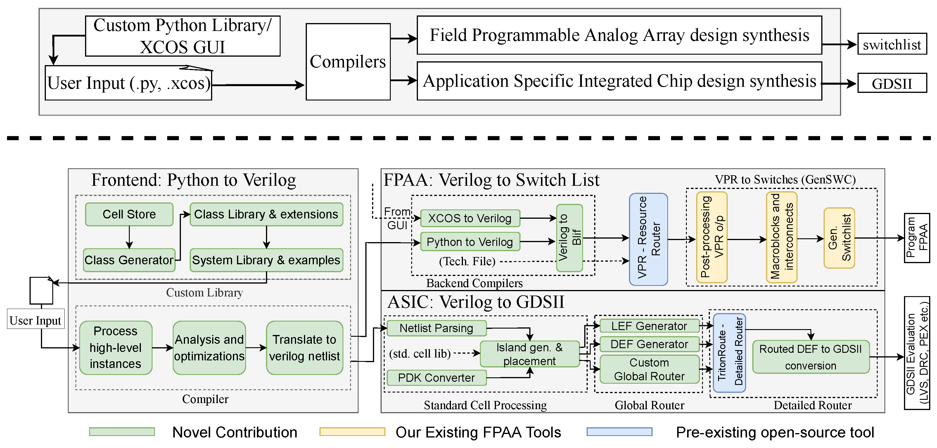
This effort looks to develop a high-level analog/mixed-signal synthesis tool (
Figure 1), utilizing the decades of development in digital synthesis, that uses and builds upon the unique aspects of analog computing capabilities. Digital synthesis, including both FPGAs and custom ICs, from high-level representations (e.g., Python, MATLAB, Verilog) has become a common and familiar practice for digital IC design and targeting of FPGA devices, enabling tool abstraction for compiling from such representations [
7] as well as research into automated generation of digital standard cells [
8]. Digital standard-cell libraries are ubiquitous for custom digital IC design. Open-source (e.g., LegUp [
9]) and commercial (e.g., Vitis HLS [
10]) tools arose from the efforts of customized high-level compilers for rapid accelerator design. Recent Multi-Level Intermediate Representation (MLIR) [
11] efforts aim to build reusable and extensible compiler infrastructure [
12] including algorithm-centric Python-based programming and synthesis flow for FPGA [
13] and IC synthesis [
14].
In contrast, analog synthesis for analog system design and analog computing is nearly non-existent. Initial efforts in analog synthesis often focused on low-level analog components, such as creating an op-amp or similar low level of circuit complexity [
16,
17,
18,
19,
20]. Recent interest in analog tool development follows these directions [
21,
22,
23], building only a few blocks (e.g., current source, differential pair) to make a small analog component (e.g., amplifier, small data converter). A different approach more consistent with digital synthesis for targeting configurable devices and new ICs requires a different approach built upon recent efforts in analog computation abstraction [
24]. Recent efforts in FPAAs [
4,
25,
26,
27,
28], particularly computational analog blocks (CABs) and CLBs within a dense Manhattan routing fabric (e.g., [
4]), created the initial pressure to develop analog synthesis tools [
29], building on VPR/VTR [
30] to actualize system level designs, leading to recent work in programmable analog standard cells [
31].
This effort focuses on developing the first integrated toolset (
Figure 1) enabling synthesis from a high-level description (e.g., Python, XCOS) to a targeted programmable analog/mixed-signal computation large-scale Field Programmable Analog Array (FPAA) and/or Integrated Circuit (IC) layout (GDSII). This tool (
Figure 1) provides a unified Python framework, as well as XCOS GUI description, for targeting an FPAA as well as IC layout generation, creating a lightweight (∼MBs), easily installable tool without dependencies on other projects, enabling the development of programable analog island blocks enabling floor planning and placement. The FPAA targeting builds upon initial FPAA analog tools [
29] (e.g., GenSWC: our local CAB/CLB place and route Python tool to create a targetable switch list) including the open source VPR toolset [
30] with additional components developed for this effort (
Figure 1). The simplicity of island architecture channels enables a faster global router with low-order polynomial (vs. exponential) time complexity. Although this discussion focus on the difficult analog and digital interfaces, this mixed-signal tool is capable of digital component integration. The tool chain (
Figure 1) integrates with pre-existing tools to expand the wider open-source ecosystem.
The parallel development of the formalization of analog computation leading to technology-applicable benchmarks [
32] and programmable analog standard cells [
31,
33] are two important parallel developments enabling this toolflow development, further differentiating this toolflow from other approaches. The abstraction and formulation of analog computation enables meaningful analog system benchmarks, enabling tool-based architectural design space exploration to determine the best analog/mixed-signal computing architectures [
32]. Ongoing current efforts on fast simulation for analog verification will be essential to the design exploration, although beyond the scope of this effort. The acoustic benchmark (Case I) [
32], an end-to-end embedded speech classifier, is used to illustrate our tool, where all of these benchmarks (acoustic, vision, communications, and filters) are relevant for these tools and will be part of later efforts. The recent development (and ongoing development in several IC processes) of programmable analog standard cell libraries [
31,
33], with standard CMOS Floating-Gate (FG) devices enabling programmability (e.g., 14 bit, 10 year lifetimes [
34]), allows for these tools to use a digital synthesis (
Figure 1) for analog synthesis components. The toolflow that synthesizes layout (to a GDS file for fabrication) utilizes recent standard cell libraries [
33,
35], using these components in a flow similar to digital synthesis (
Figure 1) but with a floating-gate aware design flow. Analog programmability reduces the block complexity of an analog library, not relying on a huge number of blocks setting parameters (e.g., bias currents) through multiple transistor sizes. Creative uses of digital standard cells for analog design (e.g., [
36]) to enable some synthesizable analog simply expand the available capabilities. This effort drastically decreases the design time, design cost, and design uncertainty of system analog/mixed-signal ICs, potentially opening up a technology-independent foundation to automate analog design, as well as making greater energy efficiency optimizations possible.
This analog and mixed signal HLS compilation from a Python- or XCOS-level description (
Figure 1) is the focus of the following sections. After reviewing current efforts in FPAAs and programmable analog standard cell concepts (
Section 2), the discussion starts with the syntax descriptions and extensions required for the tools (
Section 3,
Figure 2), including Python descriptions (
Section 3.1) and Verilog descriptions (
Section 3.2). The discussion first develops the FPAA-targeting algorithms to convert Python or XCOS High-Level Synthesis (HLS) to switch list (
Section 4), including lowering Python code to Verilog (
Section 4.1), lowering Graphical XCOS to Verilog HDL (
Section 4.2), compiling Verilog to a switch list (
Section 4.3) with vectorized representations (
Section 4.4), and addressing the challenges of this compilation (
Section 4.5). The discussion continues by developing the IC synthesis-targeting algorithms (
Section 5) using these programmable analog standard cells including the netlist and GDS parser (
Section 5.1), the LEF and DEF generator (
Section 5.3), the first-pass global router (
Section 5.4), and the final routed DEF to GDSII converter utilizing open-source TritonRoute (
Section 5.5). The discussion then demonstrates the tool using the acoustic classifier benchmark [
32] for the FPAA targeting as well as IC GDS generator (
Section 6).
2. FPAAs and Analog Standard Cells
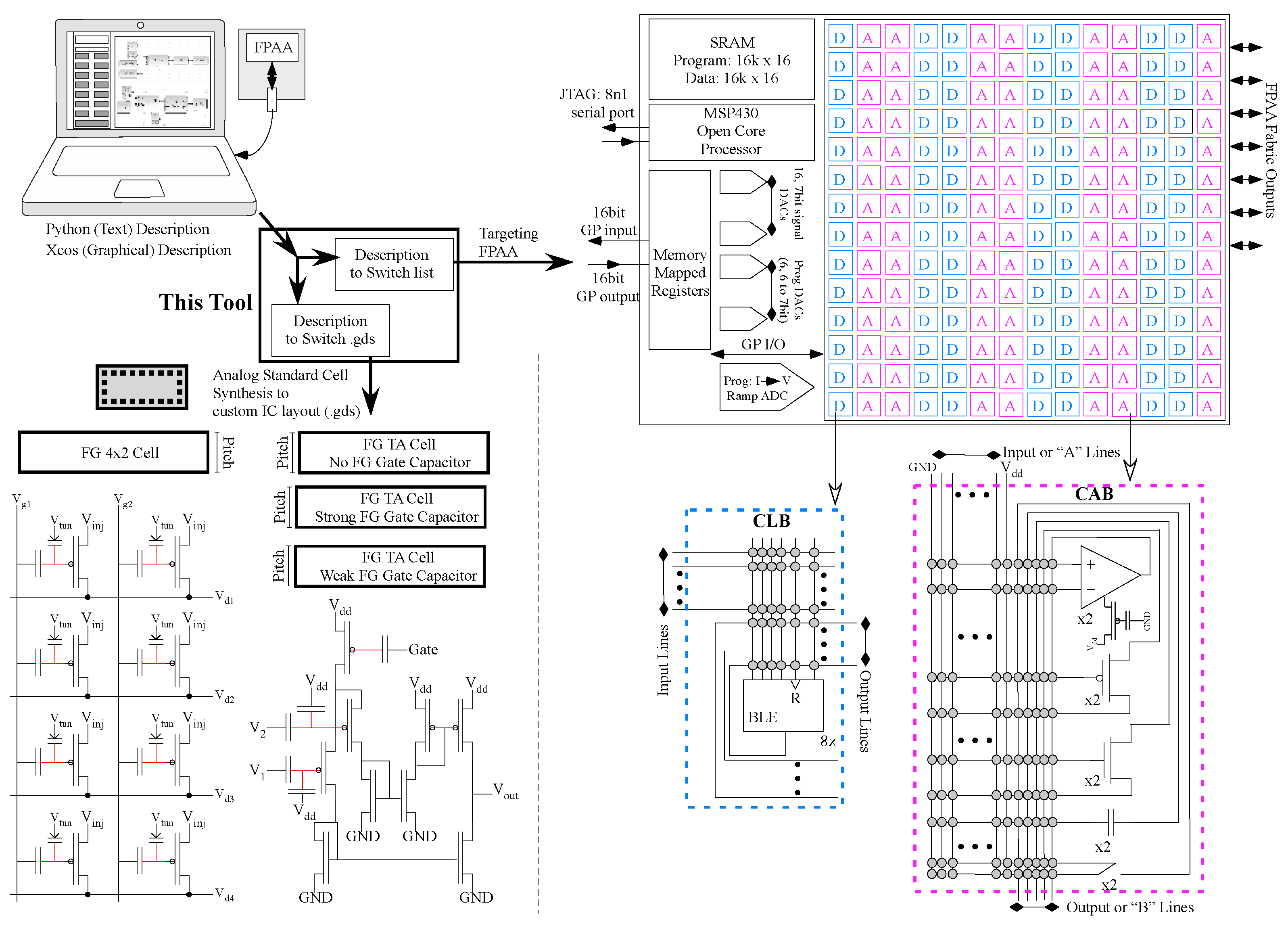
The first discussion overviews FPAAs and analog standard cell approaches, as our analog synthesis tool utilizes recent FPAA devices as well as recent programable analog standard cell developments. The SoC FPAA (
Figure 2) and earlier families of FG-enabled FPAAs demonstrated a number of core concepts, as elucidated from early large-scale FPAA techniques in 2002 to today’s devices [
4]. FPAAs have analog components plus routing between analog and digital components, similar to FPGAs. Early programmable analog arrays [
38,
39,
40] and early commercial devices (e.g., EPAC [
41] or Anadigm [
42]) were useful for
glue logic and small occasional computations. Today’s FPAAs show considerable capabilities in ultra-low power computation, signal processing, and embedded machine learning [
4] from ICs fabricated in a 350 nm CMOS process. Programmable analog FG techniques have demonstrated precision components [
4] built on work enabling programmable design for temperature [
43].
As predicted by Mead [
1], analog computing techniques result in a 1000× improvement in power or energy efficiency and a 100× improvement in area efficiency compared to digital computing. Computation in routing [
4] enables 1000× improvements in computational energy efficiency compared to custom digital [
4] and retains the custom analog computational energy efficiency [
2] on an FPAA. The emerging demand for low-power high-efficiency analog and mixed-signal computing (e.g., computation-intensive machine-learning applications) requires real-time to near-zero latency computing for ultra-low-energy applications.
Large-scale programmability is essential for these FPAA devices and is typically instantiated using analog-programmable FG devices available in standard CMOS for the memory and routing elements. Today’s SoC FPAA [
44] utilizes 600,000 programmable parameters in 350 nm CMOS. Analog programming of the single FG pFET device fabric enables computation in routing fabric as well as CAB elements [
4]. FG parameters tend to provide a 1000× advantage over other silicon memory approaches at roughly the 8–10-bit level [
4]. FG devices have demonstrated longevity (10 year lifetime) across multiple IC processes from 2
m to 40 nm linewidths [
4] with precision (e.g., 14-bit) targeted (re)programming of heterogeneous arrangements of FG devices [
34]; FG devices enable directly eliminating mismatch or setting desired targeting values in the configurable structure.
An analog standard-cell library (
Figure 2) is the first step to synthesize large analog systems to IC layout, building on digital standard cell designs and their resulting abstractions. The development of analog standard cells follows from the abstraction, CAB evolution, and hands-on use of these FPAAs [
31]. Early FPAA design tool development [
4] gave the user an initial ability to create, model, and simulate analog and digital designs. Analog design tools before these FPAA tools have a brief history, including theoretical analog automation tools, as well as early FPAA ICs [
45,
46,
47,
48,
49]. Macromodeling techniques, such as making a simplified algebraic or numerically simple ODE circuit model, remain a key framework for analog design [
50,
51]. Some techniques are coupled with digital tools for joint analog and digital system verification [
52,
53]. Custom analog IC design has little additional tool support other than low-level IC design tools. Many companies (e.g., [
18]) have tried to automate the analog design process but failed because the solution was aimed at analog IC designers who are artistic critics of other analog designs.
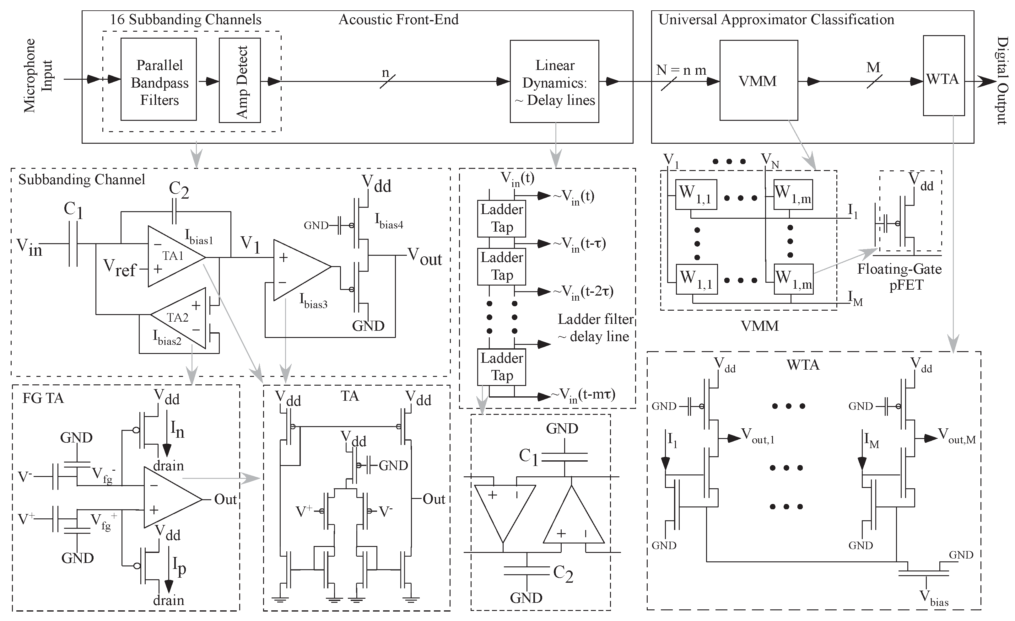
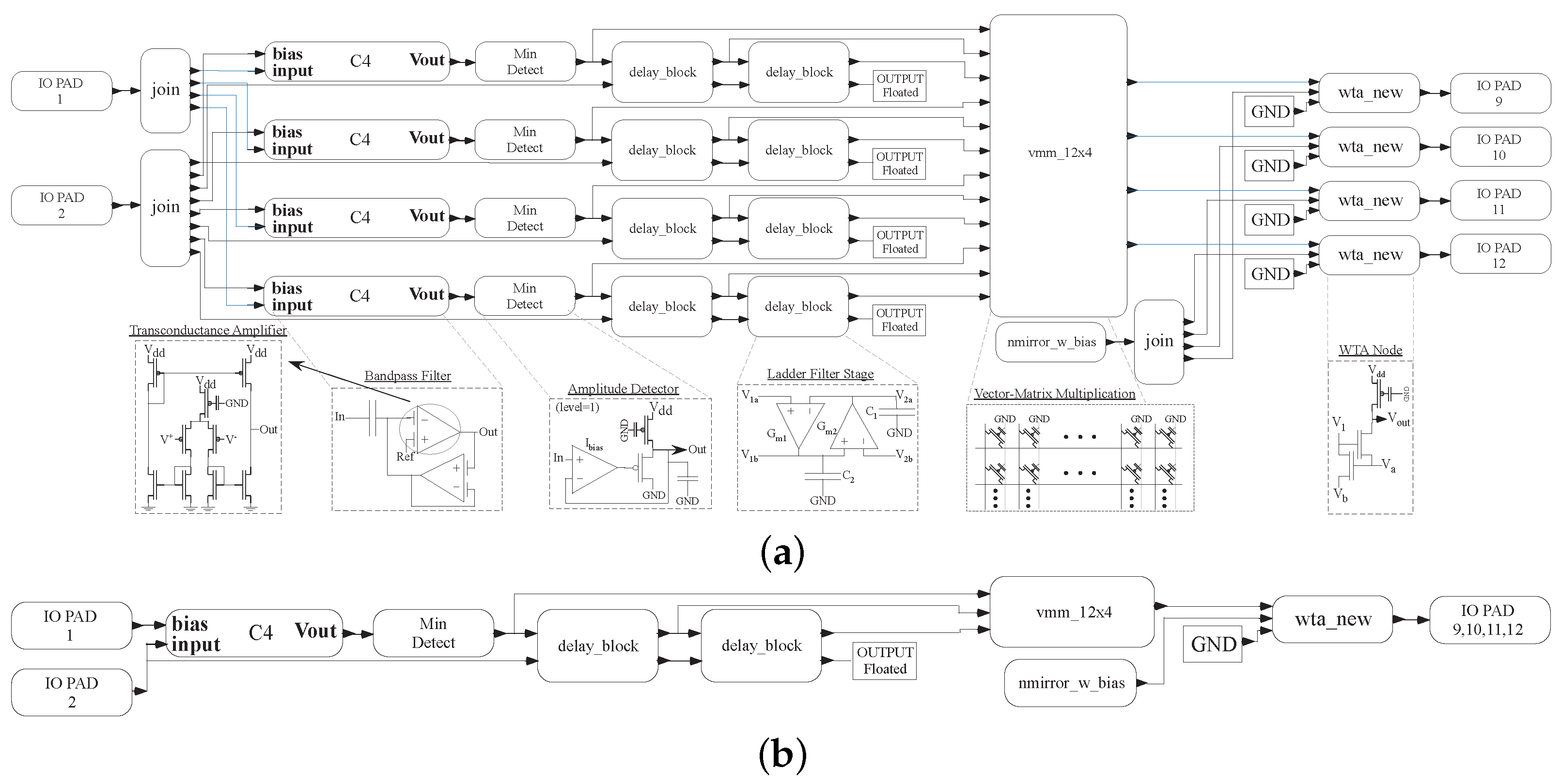
The acoustic benchmark (Case I, [
32]) is a small vocabulary (e.g., 2–5 word) command word classifier (
Figure 3). Multiple hand-designed and targeted limited versions of this application have been demonstrated on the SoC FPAA device [
44,
54]. The analog front-end blocks utilize tunable C
BPF and resulting amplitude detectors and delay blocks followed by a Vector-Matrix Multiplier (VMM) + Winner-Take-All (WTA) classifier block. The VMM + WTA classifier is a universal approximator in a single neural network layer [
54]. The VMM weights are programmable and can be trained off-line or using this embedded system.
3. Python and Verilog Syntax Descriptions and Extensions
Analog synthesis requires designing circuits at different levels of abstraction. The tool takes user-generated high-level analog systems in the Python language and automatically generates Verilog code and lower representations for FPAA prototyping and ASIC synthesis. We choose the Python language implementation for four main reasons.
Ease of use: Python’s syntax is simple and intuitive, and it offers a large number of libraries to cooperate with when designing FPAA circuits (e.g., Numpy).
Productivity: Python’s high-level abstractions and built-in data types make it possible to write concise and expressive code. This can result in faster development times and fewer errors than writing HDL code.
Flexibility: Python is a versatile language that can be easily tweaked to accommodate FPAA syntax flow. In addition, as an interpreted language, its on-the-fly execution can enable dynamic and interactive programming for the FPAA compiler.
Integration: Python has excellent portability, which makes it easier to integrate with other programming languages and tools.
Not all Python descriptions would be possible at this stage for the resulting synthesis, as well as initial further tool development. At this time, the Python tool allows for functions of various blocks, as well as it allows for Python to be used to calculate parameters and values that would be inserted into these functions. In time, other functions will be enabled into this compilation. This section describes the tool flow and the introduced syntax extensions to the Python (
Section 3.1) and Verilog languages (
Section 3.2).
3.1. Python Interface
The Python interface requires considering the unified cell library, class library & extensions, and system library.
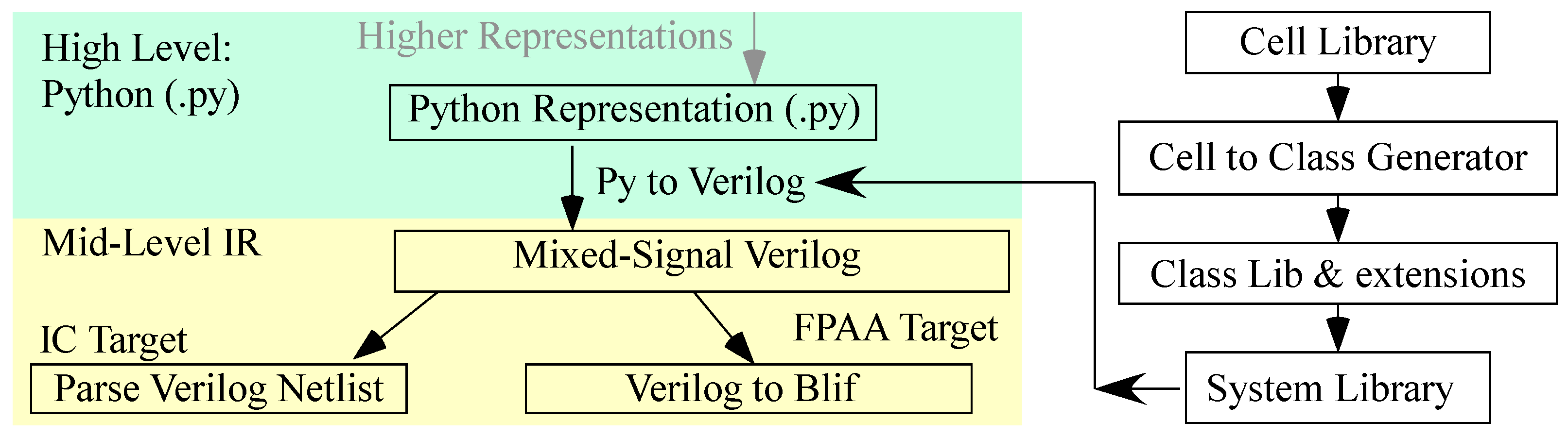
Unified Cell Library starts the Python flow (
Figure 4), holding information on programmable FPAA building blocks and standard cell library designs. The blocks store parameterized information (e.g., FG biases) while the cells store pin and process node information (Listing 1). Building blocks and standard cells alike can be updated by users as the need arises.
| Listing 1. Example of FPAA blocks and ASIC cells in cell library. |
{"C4":{"type": "FPAA", "board": ["3.0", "3.0a"],"Gain_Bias":3e-6," Gain_Bias_n":1e-6,"Gain_Bias_p":1e-6,"Feedback_bias":"3e-9"," Feedback_bias_n":"1e-9","Feedback_bias_p":"1e-9","num_caps":"6"}, "Scanner": { "type": "ASIC" , "process": ["65nm"], "pins": ["INPUT1_1", "INPUT1_2", "INPUT1_3", "INPUT1_4", "RESET_B_1", "OUTPUT", "CLK1", "D", "VPWR", "GND"] } } |
Class library and extensions abstract the information from the cell library in the form of Python classes that can be instantiated as objects during use. The tool (Listing 2) automates the creation of base Python classes, enabling easy user updates to the cell library. The extensions allow for further customization that can be made by expert users, which will be unaffected by automated updates to the base classes. Modifications from simplified mapping of pins to FG bias calculation from a given specification can be implemented and executed by the compiler.
| Listing 2. Example of class-level abstraction and extension. |
# Base: class_lib.py class BPF(std_cell): def __init__(self,input, num_instances = 1, cell_type = ’ASIC’, colsel2 = None, colsel1 = None, gate1 = None, out = None, gate2 = None ): self.colsel2 = colsel2 self.colsel1 = colsel1 self.gate1 = gate1 self.out = out self.gate2 = gate2 # Extension: class_lib_ext.py class BPF(BPF): def __init__(self, input, num_instances = 1, cell_type = ’ASIC’, select = None, gate = None, output = None ): super().__init__(input, num_instances, cell_type) self.colsel2 = select[0] self.gate1 = gate[0] self.colsel1 = select[1] self.out = output self.gate2 = gate[1] class LPF(LPF): def set_center_freq(freq): c_cap = 10e-12 Gm = 2*3.1415*freq*c_cap Ut = 25e-3 kappa = 0.8 self.Feedback_bias = (Gm*2*Ut)/Kappa |
System Library and Main Program define the larger scale applications from the blocks and cells described above (Listing 3). For FPAAs, blocks comprise either a single element or multiple connected elements within a CAB or multiple CAB blocks. The blocks in the cell library give a sufficient overview of the blocks required for synthesis, where further discussion of designing CAB blocks is described elsewhere [
29]. For custom IC layout, a similar gathering of standard cells into an
island architecture enables effective placement and routing within an island and in a larger design, as initially introduced [
31]. FG cells can utilize multiple FG elements, resulting in tight routing that is not desirable to enforce on non-FG-based cells and the resulting routing tracks. The FG cells with tight routing are grouped together on one side of the island, and the non-FG cells are grouped together on the other side. Cells that are a combination of FG and non-FG cells are placed in the middle. These islands create single-use modular functions enabing standard place and route for the larger custom IC design. These techniques will be the subject of future publications, although this description is sufficient for the algorithms in this discussion.
| Listing 3. Vectorized example of an embedded speech classifier system and the compiler API. |
# FPAA_system_examples.py import class_lib_ext as fg def alice_vectorized(): inpad1 = fg.inpad([1]) inpad2 = fg.inpad([2]) c4_out = fg.c4_sp([inpad1, inpad2], num_instances=4, Gain_Bias=[0.00003, 0.00004, 0.00005, 0.00006], Gain_Bias_p=np.arange(0.0001, 0.0005, 0.0001)) min_det_out = fg.Min_detect(c4_out, num_instances=4) gnd = fg.gnd() [delay_stg1, delay_stg2] = fg.delay_block([min_det_out, gnd], num_instances=4)() [delay_stg3, _] = fg.delay_block([delay_stg1, delay_stg2], num_instances=4)() vmm_out = fg.vmm_12x4([min_det_out, delay_stg1, delay_stg3], num_instances=4) nmirror_out = fg.nmirror_w_bias(nmirror_out) wta_out = fg.wta_new([vmm_out, nmirror_out, gnd], num_instances=4) outpad = fg.outpad(wta_out, [9, 10, 11, 12]) # Main.py import FPAA_system_examples import fg_compilers as fc fc.fpaa_compile(alice_vectorized) |
3.2. Verilog Interface
The Verilog interface code is extended for FPAA and ASIC Verilog definitions.
FPAA Verilog is extended from standard Verilog for handling analog circuits (Listing 4). The FPAA targeting requires programming parameter handling in addition to net connections. The FPAA Verilog file contains a module-by-module definition for each component. Each module starts with the module name declaration, the input and output net names (as applicable), the parameter declarations (extended from standard Verilog), and an “endmodule” statement. In standard Verilog, the “assign” statement is used to declare net connection or logic outputs; this tool uses “assign” statements to define programming parameters, something that does not exist in digital definitions. Each parameter is handled by a single “assign” statement by assigning a value to each parameter name. In a vectorized multiple block setting, the parameters are assigned as a list to a parameter name.
| Listing 4. FPAA Verilog excerpt describing a vectorized minimum detection circuit routed to four input and four output pads on the FPAA. |
module pad_in(); output [3:0] net1; assign pad_num = [1,2,3,4]; endmodule
module Min_detect(); input [3:0] net1; output [3:0] net2; assign block_num = 4; assign Min_detect_ls = [0,0,0,0]; assign Min_detect_fgswc_ibias = [5.000D-086,6.000D-08,7.000D-08,8.000D-08]; assign Min_detect_ota0_ibias = [0.000002,0.000003,0.000004,0.000005]; endmodule
module pad_out(); input [3:0] net2; assign pad_num = [5,6,7,8]; endmodule
|
ASIC Verilog compilation utilizes additional parameters required for the GDSII placement and routing synthesis flow, including the relative location of the cell within its island and the connections (Listing 5). Each cell is called a module instance with relevant information passed as parameters. The island number defines which group of cells that particular cell shares FG infrastructre with while row and column communicate the horizontal and vertical offsets within the group. This syntax also extends to vectorized blocks that refer to a matrix of cells, indicated by the matrix row and matrix column fields. Routing nets are identified by shared net names, which connect two or more terminals across multiple cells.
| Listing 5. ASIC Verilog excerpt describing standard cell islands and their connections. |
module TOP(); GateMuxSwc_Tile I__7 (.island_num(0), .row(2), .col(4), .matrix_row(1), .matrix_col(6)); GateDecoder I__9 (.island_num(0), .row(1), .col(4), .sigin0(c_net0), ... , .sigin11(c_net11)); AFE I__10 (.island_num(1), .row(1), .col(1), .sigout0(c_net0), ... , .sigout11(c_net11)); endmodule |
4. FPAA Flow Algorithms: Python High-Level Synthesis to Switch List
With the code structure, extensions, and syntax established, the discussion focuses on the lowering and compiling code for the FPAA targeting and IC synthesis. This section describes the algorithmic process by which high-level Python descriptions are turned into a switch list targeting specific transistors to be programmed on a reconfigurable analog device (FPAA). The Python syntax, building on native Python syntax, has particular extensions, parameters, and procedures for the resulting algorithms for FPAA and IC layout generation. While the defined FPAA Python syntax passes native Python syntax checks, it may fail semantic checks in some cases. The discussion develops the FPAA targeting algorithms to convert Python or XCOS High-Level Synthesis (HLS) to switch List (
Section 4), including lowering Python code to Verilog (
Section 4.1), lowering Graphical XCOS to Verilog HDL (
Section 4.2), compiling Verilog to a switch list (
Section 4.3) with vectorized representations (
Section 4.4), and addressing the challenges of this compilation (
Section 4.5).
4.1. Lowering Python Code to Verilog
The core principle of the FPAA HLS compiler is to maximize the use of native syntax and resolve any special cases. The conversion process (Algorithm 1) is decomposed into three steps:
| Algorithm 1 Algorithm to lower Python high-level representations to Verilog |
- 1:
- 2:
- 3:
for each node n in do - 4:
if n is regularCell then - 5:
- 6:
- 7:
else - 8:
- 9:
- 10:
- 11:
end if - 12:
end for - 13:
- 14:
for each in do - 15:
if is vectorizedBlock then - 16:
- 17:
else - 18:
- 19:
end if - 20:
end for - 21:
|
An Abstract Syntax Tree (AST) is a data structure used in computer programming that represents the syntactic structure of source code in a tree-like format. As an intermediate representation, AST provides a hierarchical way to access different levels of code components recursively. By traversing the AST, the converter can extract every wanted detail appearing in the syntax and discard redundant details. The translation should guarantee the net interconnection correctness to ensure the desired functionality.
The symbol table allows the compiler to keep track of the objects used in the program and their corresponding properties. By going through the symbol table, the compiler can also detect errors in semantics analysis. Simultaneously with symbol table generation, the net assignment must also be completed to ensure correct block interconnection (more details in
Section 4.5). To take advantage of the powerful native Python interpreter, the FPAA compiler takes two-way paths to maintain the symbol table.
Interpreter path: For most standard cells whose definitions do not violate the native syntax and semantics rules, the FPAA compiler calls the Python interpreter to construct corresponding standard cell objects and then creates new entries in the symbol table.
AST parsing path: For certain hardware-specific standard cells, their syntax has implications for hardware implementation. This means they are legal in a hardware context but fail native Python semantic legality checks. For example, the nmirror cell outputs the same variable as the input. In Python syntax, this would be expressed as , which does not make sense in Python since variables cannot be referenced before declaration. Therefore, the FPAA compiler parses special cases and handles them accordingly for the symbol table.
Once the compiler generates the symbol table, it has all the information needed to reconstruct the Verilog code. The code generation process handles two main aspects to ensure consistency between Python and Verilog code.
Semantic analysis: Semantics analysis in the FPAA compiler checks net assignment correctness and resolves possible vectorization based on the design;
Reformatting: Verilog has a parallel programming paradigm, unlike high-level languages that are sequential. To address this discrepancy, reformatting Verilog code is crucial to ensuring accurate translation.
4.2. Lowering Graphical XCOS to Verilog HDL
Because XCOS files are stored in XML, an object-oriented text format, they can be extracted into objects (nets, blocks) with a built-in Python package. This built-in XML parsing tool generates a tree structure with all the XCOS objects consistent with object-oriented programming. The two most important objects in this conversion are blocks and explicit links. Blocks are actual block components, and explicit links are net connections. Each block and net object includes its own unique id and parent id. The block objects also include the block name and block parameter values. The algorithm (Algorithm 2) iterates through the entire XCOS file, finds all the net connections and their parent blocks, and finally writes the Verilog output module by module based on the connections.
4.3. From Verilog to Switches
The Verilog file is lowered to an extended Blif file definition for FPAA targeting [
29], and passed to VPR [
30] for global FPAA place and route to generate the switch list. The switch list defines the physical FPAA programming. Our tool uses a lark-based Verilog parsing package to generate a Blif file from the Verilog definition by parsing all the modules into objects and listing every object. The Verilog format describes the circuit module by module for a straightforward conversion to Blif (Algorithm 3). The Blif file passes through VPR to generate the global CAB routing. The FPAA architecture details in XML format are supplied to VPR with the Blif file. VPR generates a placement file (.place), a packed netlist file (.net), and a routing file (.route), which are passed to GenSWCS code [
29] to produce a switch list to program the FPAA.
4.4. Circuit Vectorization
Vectorization in Verilog refers to defining multi-bit signals or data types using vector notation, enabling Verilog designers to efficiently create complex data types and signals. Python’s array operations serve as counterparts to vectorization using arrays or lists. Vectorization enables more expressive code, reducing the manual effort required for large system design. The improved readability can facilitate addressing error-prone issues and benefit code review and debugging.
| Algorithm 2 Algorithms to lower XCOS high-level representations to Verilog. |
- 1:
for each net id do - 2:
- 3:
if split wire then - 4:
- 5:
end if - 6:
end for - 7:
for each module do - 8:
for each net do - 9:
if net parent equals module input then - 10:
- 11:
end if - 12:
if net parent = module output then - 13:
- 14:
end if - 15:
end for - 16:
for each block parameter do - 17:
- 18:
end for - 19:
- 20:
end for
|
| Algorithm 3 Algorithm to lower from Verilog to Blif |
for each input pad do end for for each output pad do end for for each module do end for
|
Vectorization of the acoustic classifier benchmark system significantly reduced code size. The original Python code spanned 37 lines and 2095 characters. The corresponding Verilog code used 303 lines and 5888 characters. After vectorization, the Python code decreased to 11 lines and 776 characters (70% fewer lines, 63% fewer characters). The Verilog code decreased to 95 lines and 2761 characters (69% fewer lines, 53% fewer characters). Compared to Verilog code, Python code for Alice compressed Verilog code by 88% in lines and 72% in characters. Undoubtedly, the vectorized FPAA Python high-level synthesis significantly enhanced the code expressiveness.
4.5. Challenges in Conversion
The semantics gap between Verilog and Python can overcome key challenges:
Special case handler: Most special case challenges come from the hardware intrinsic that is illegal in high-level programming, e.g., the nmirror case mentioned in
Section 4.1. Some other special cases are because of uniqueness in the standard cell. For example,
and
cells do not have an input net. These unique standard cells can be handled by AST parsing path (also in
Section 4.1).
Net assignment: Correct net assignment is essential for determining the correctness of block interconnections. A reliable symbol table avoids problems such as duplicate net assignments, unassigned nets, and false net references. In addition to a well-maintained symbol table, semantic analysis during code generation also plays an important role in resolving net assignment problems such as unassigned entries.
Standard-cell-aware vectorization: Vectorization depends on semantics and standard cell features. Since cells have varying I/O nets, the input may exceed cell requirements. Thus, input net slicing must account for standard cells. Special cases also pose challenges, such as (=0 V) cells, which have only one instance that can be shared by all standard cells, requiring vectorization based on the connected standard cell.
5. IC Synthesis Flow Algorithms
The ASIC compiler converts Python objects into the ASIC-specific Verilog syntax as defined in
Section 3.2. A combination of the Verilog file, a standard cell library, and a Process Design Kit (PDK) are fed to the GDS synthesis modules to generate the final result. The PDK is specified as an LEF file from any example cells in the process and a layer map describing the stack of said process. Optionally, given PDK information of two compatible process nodes (i.e., similar geometry), standard cells could be converted between processes using the built-in PDK converter. Common layers can be remapped and contact sizes adjusted to match the destination format. The discussion develops the IC synthesis targeting algorithms (
Section 5) using these programmable analog standard cells including the netlist and GDS parser (
Section 5.1), the LEF and DEF generator (
Section 5.3), the first-pass global router (
Section 5.4), and the final routed DEF to GDSII converter utilizing open-source TritonRoute (
Section 5.5).
5.1. Netlist and GDS Parser
The initial step takes in a Verilog file and uses a lark-based parser to extract module instantiations and parameter information from the input netlist. A preprocessing step generates a unique list of instantiated modules to allow for multiple calls to a cell. This enables the next phase, which is GDS parsing. The binary format of the file is converted to text, which contains records of all individual polygons making up subcells and connections within the cell. The highest level module is then reconstructed by calculating the dimensions of all subcells, pulling in previously defined cells when needed. This process also extracts pin information of the top cell, accounts for rotated or mirrored subcells, and avoids redefining reused cells, as that would violate the GDS standard. This process of reconstruction allows arbitrary standard cells to be recombined into larger GDS files, which are later used for placement. This cell information is parsed into a data structure that the island generation algorithm uses.
5.2. Island Generation and Placement
The grouping of tightly related cells to share peripheral circuits, particularly FG cells, brought forth the idea of an island approach. Islands consist of a gradient of heavily FG-dependent cells to cells with no FGs at all. These cells are designed to abutt for space efficiency and to reduce routing complexity. The FG cells require additional control lines for programming and operation, as well as row and column program select lines. Non-FG cells benefit from having additional available routing tracks. During FG programming, including parallel island programming, the circuits collapse into a programmable crossbar array.
A preprocessing step sorts cells into separate islands, and these islands are arranged to place the bottom left cell at the first position (Algorithm 4), allowing the row-based structure of the placement algorithm to work upwards from the cell that is least likely to be missing. The tool handles column width estimation for placing matrices (or cells) in an offset position and places all sub-islands while storing all cell and sub island locations. Sub islands refer to situations where die dimensions do not allow for all cells to abutt, requiring cells who share nearby signals to route to each other. For example, a decoder tree for gate side control might not fit vertically within the allotted space for core island height.
| Algorithm 4 Algorithm to lower from Verilog to GDS: cell and island placement |
- 1:
Input: Island data structure, cell data structure - 2:
cell pre-processing on island structure - 3:
for each Island do - 4:
Reset previous cell and island size tracking - 5:
for cell in Island do - 6:
retrieve cell size and relative placement - 7:
Track column widths for offsets - 8:
Calculate x and y from relative placement - 9:
Place the coordinate of the corner instance - 10:
if Cell is matrix then - 11:
Considering overlap and separation - 12:
Find last coordinate in columnar direction - 13:
Find last coordinate in row direction - 14:
end if - 15:
Update cell placement & island size - 16:
end for - 17:
Calculate exact island placement - 18:
end for
|
5.3. LEF and DEF Generator
Given a process technology LEF, the task is to generate the design LEF file. The module inserts the appropriate technology LEF specification for the current design and adds in all pin definitions extracted from GDS. New standard cells in the same process require only a GDS file, and not a new LEF file. To create a DEF file for a design, the module specifies database units, die size, and track spacing. It generates tracks based on die space and track size. Component placement and blockages (i.e., metal shielding, up to stop layer, over cells to prevent routing) are also handled. Parsing of all nets and generation of correct instance-pin connections for both matrices and single cells are taken care of as well.
5.4. Global Router
A custom track-based global router is used to generate a guide file for all nets defined in the DEF file. Given an instance name and net, it will figure out the location of the pin either within a matrix or as a cell. A bounding box will then be generated to extend the pin outside the cell if needed. This creates a directional access pattern for the net connections. Access patterns are either horizontal (top or bottom facing pins) or vertical (left or right facing pins). In the sub case of up/down, the metal stack also exists, but once an appropriate metal layer is reached, the access patterns return to the previous two cases. A net will consist of any arbitrary combination of pins following the defined access patterns. To route a net, the tool will pick an empty track aligned with the globally defined track spacing and extend across all pins orthogonal to that routing direction. If pins on the net exist outside the current channel, the tool moves into the subsequent channel to connect said pins along a selected track in the new routing direction. The global router also extends this approach to handle padframe routing. Nets connected to a frame and multiple pins would first have the detailed pin connections handled by the approach described above then extend into the global track space where they are routed to a frame.
An alternative approach considered was to construct a Minimum Spanning Tree (MST) for each net, decompose it into two terminal points using Steiner decomposition, and use a heuristic search algorithm such as A* pathfinding to connect the points. However, there are two main reasons for why this approach was not chosen. The first is that our island architecture approach lends itself to creating a heavily channel-based structure where tracks are convenient, and the second is that heuristic approaches such as A* tend to be very memory-intensive, and worst-case time complexity grows at a rate of , where d is the depth of the solution and b is the branching factor. This approach is commonly used in contemporary routing tools and contributes to the long run times to generate a connected solution. In contrast, the track-based approach has a worst-case time complexity of , where N is the number of tracks in the routing direction and P is the number of polygons already placed. As for space complexity, it only keeps track of placed polygons as opposed to all possible solutions when searching for an optimal solution in unbounded A*. Ultimately, the effort put into standard cell designs abutting and the island architecture create a situation where one need not pay the costs of the alternative approach to guarantee a solution.
5.5. Routed DEF to GDSII Converter
The detailed router (TritonRoute [
15]) produces a routed DEF file that needs to be converted to a final output by merging with the GDS file generated during placement. This module parses routed nets and creates polygons in the output GDS (Algorithm 5). The routed DEF only produces a path, so net thickness, metal layers, and contact definitions need to be added. Extra parsing of the LEF file is required for unspecified contact information that may not have been provided as output in the DEF file. Once this step is completed, the final GDSII layout is created.
| Algorithm 5 Algorithm to lower from Verilog to GDS: DEF to GDSII converter |
- 1:
open DEF file - 2:
for record in Def file do - 3:
if Via definition then - 4:
update Def via data structure - 5:
end if - 6:
if Routed Net then - 7:
Convert net trace to GDS polygon - 8:
if Via on net and defined in Def then - 9:
Look up via in Def defined list - 10:
else Via defined in Lef - 11:
Parse Lef file to find via definition - 12:
end if - 13:
end if - 14:
end for - 15:
open gds file and insert polygon gds record in top level design
|
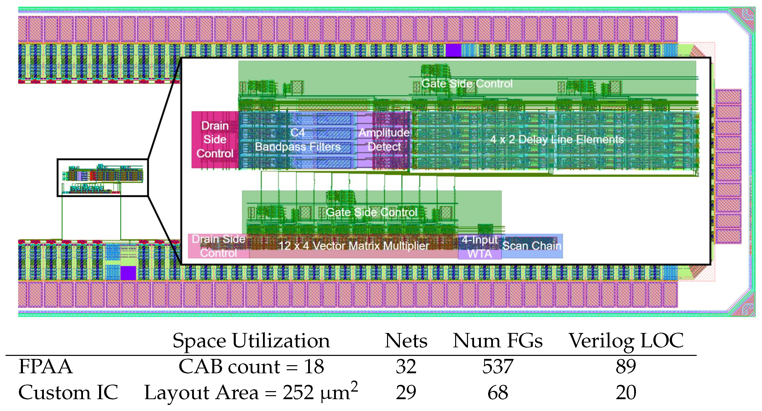
6. Tool Demonstration Using the Acoustic Classifier Benchmark
The tool capabilities are demonstrated by compiling the acoustic classifier benchmark (
Figure 5 and
Figure 6) from a high-level representation to a switch list for an FPAA design as well as a GDS file for IC fabrication on a 65 nm CMOS process with internally designed FG-based standard cells (
Figure 7). One of the formulations of the benchmark was generated in XCOS (
Figure 5) to demonstrate the XCOS tool flow. The computational flow included four frequency band frequency decomposition, amplitude detection, ladder-filter delay stages, and embedded classification through a vector-matrix multiplication and winner-take-all classifier [
54]) for command-word recognition. The signal path computation is analog throughout this formulation.
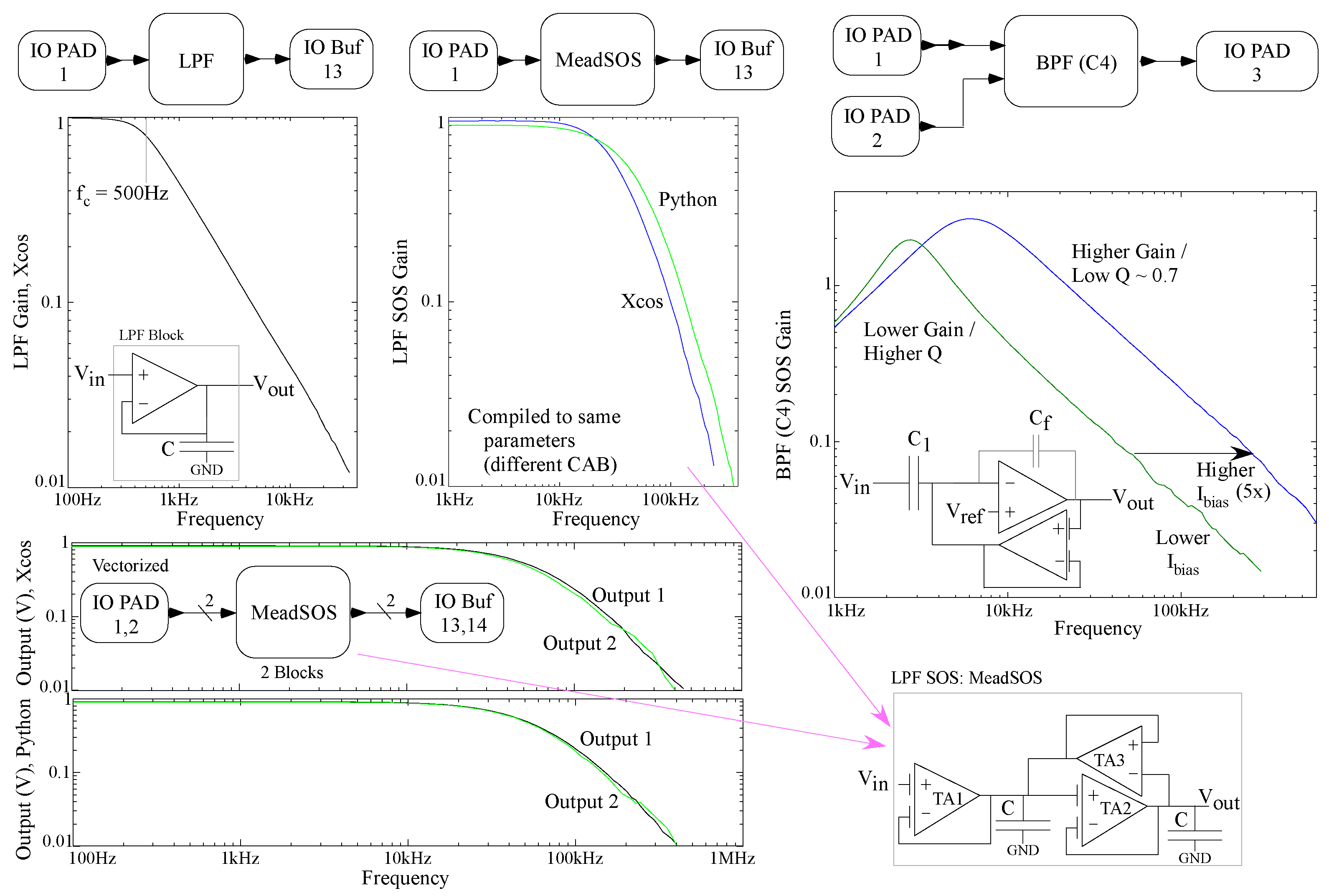
The FPAA formulation enables compilation from a high-level representation (XCOS/Python) to compilable hardware. Acoustic circuits, including first- and second-order Low-Pass Filter (LPF) as well as Bandpass Filter (BPF), composed of multiple TA elements, compile from both XCOS and Python definitions to working experimental measurements (
Figure 6). The XCOS representation (
Figure 5) and equivalent Python representation (a simple version of Case I Acoustic Benchmark [
32]) were both reduced to equivalent Verilog representations to be targeted on an FPAA, routed on the device with VPR (
Figure 7) and our GenSWC tool with identical results. The vectorized and non-vectorized representations are lowered into an expanded and flattened Blif netlist representation that directly passes to VPR for place and route in the FPAA device. The VPR routing uses a capacitance, and therefore line-length, minimization constraint, as that basic constraint also minimizes the required energy. This routing metric has been sufficient for multiple SoC FPAA designs [
44] over many years, and the tools did not require any modifications at this level. Each block in the design as well as an integrated system have been validated in previous work, and the tool’s switch list was compared to those to ensure correctness.
The acoustic benchmark is a programmable end-to-end microphone-to-symbol command-word recognition problem that requires some form of embedded Machine Learning (ML) for the solution. One of the command-word datasets (Case I) is from the TIMIT [
56] or TI digits database [
57]. This implementation utilizes a VMM+WTA universal approximator ML classifier. Typical solutions use a bandpass filterbank and amplitude detection for the incoming signals in a near exponential spacing of center frequencies (e.g., 50 Hz to 10 kHz) that model the human cochlea dynamics (e.g., [
44], preserving the highest signal and frequency information while refining the data representation). Programmability enables the parameters and classification, as well as repeatable front-end computing structures that eliminate the effect of mismatch, resulting in a near-ideal transfer function for each filter channel.
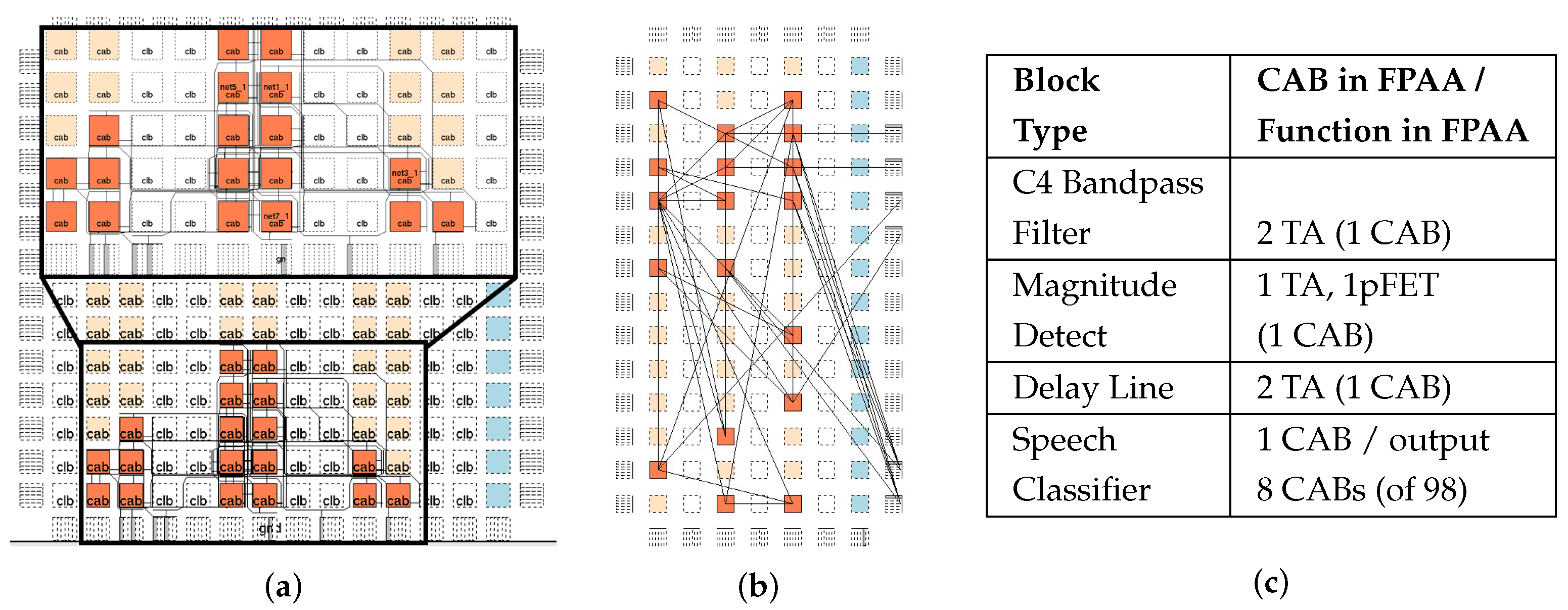
The Python representation lowered to the Verilog level was formulated into two islands for the IC synthesis (
Figure 8). The tool generated and placed both islands, and after pin definitions, the islands were fed back into the tool and routed together. The design maintained DRC rule checks starting from DRC-clean standard cells and the detailed router obeyed the technology LEF design rules to avoid violations. For usage details, the IC flow took 3.66 s with peak memory usage of 13.5 MB to generate a placed GDSII file and produce a routed guide file. The detailed router took 8:38 min with peak memory usage of 2.5 GB. Given the size of this particular IC layout with its nearly 1000 transistors, a full post-layout simulation is challenging for a real acoustic input. The need to enable large-scale simulations with realistic analog signals motivates current research in fast analog simulation tools that reasonably predict measured results building on the existing FPAA simulation tool framework [
58], similar to digital simulation tools.
7. Summary and Discussion
This work developed and demonstrated the first major step for a high-level analog/mixed-signal synthesis tool starting from a high-level description (Python and XCOS) to a physical implementation in a single toolflow. The physical implementation either provides the switch-list file for targeting an FPAA or provides the GDSII file describing a new custom IC. The HLS tool description included syntax descriptions and extensions (Python and Verilog), the lowering of Python or Graphical XCOS to Verilog, then Verilog to netlist and then to the targeted output, either the switch list for targeting an FPAA or the LEF and DEF and routed GDS for a custom IC. The custom IC synthesis utilizes recent efforts in the development of programmable analog standard cells [
31,
33]. FPAA devices enable rapid prototyping of analog circuits that is not feasible in most places today, empowered by programmable FG analog circuits. This tool creates a lightweight (∼MBs), easily installable tool without dependencies on other projects, enabling development of programable analog island blocks enabling floor planning and placement.
The tool demonstrated automatically generating GDSII layout or FPAA switch list for the acoustic benchmark (Case I) [
32] as well as some smaller circuit test cases. This end-to-end embedded acoustic classifier in both synthesis flows compiles bandpass filters, delay elements, VMM blocks, and WTA circuits using smaller elements (FG FETs and programmable TAs) as core blocks either in an FPAA device or in the programmable analog standard cells. The acoustic benchmark case is published elsewhere (e.g., [
44,
54]) on this FPAA, and the tool outputs were functionally identical to those previous designs.
This analog and mixed-signal HLS tool enables analog system design with abstraction at multiple levels of design, greatly advancing analog synthesis beyond simple blocks (e.g., current source, differential pair), creating standard analog components (e.g., amplifier, small data converter) [
16,
17,
18,
19,
20,
21,
22,
23,
23]. Our approach allows for fine-grain design (transistor-level) as well as multiple higher levels of abstraction, circuit programmable at each level, enabling a wider community to use analog design tools as compared to experienced analog designers.
This analog synthesis tool is part of a larger effort to enable design space exploration for new analog system ICs that can be a mixture of FPAA fabric and custom blocks for a range of applications (e.g., the full acoustic across a range of CMOS technology nodes through our recent development of programmable analog standard cells (e.g., 130 nm CMOS [
33] and other CMOS processes). This system optimization should include evaluation of area and resource allocation, energy and power, SNR, and delay and latency, that, in turn, require fast large analog system simulation to evaluate and eventually verify. Simulating 10 s of audio (20 kHz frequency) for a system of 1000 transistors, such as the synthesized custom IC, requires over 10
simulation nodes before even considering the complexity of SPICE circuit modeling (e.g., EKV) or the ODE simulator complexity (e.g., ODE45). Simulation of these typical 1TMAC (MAC = Multiply ACcumulate) systems is fairly impractical except on larger servers as opposed to traditional analog circuits of 10 s of transistors (typical of other analog tools [
21,
22]) with a couple periods of a sine or square wave input. In practice, these system designs will be significantly larger for acoustic classifiers, not to mention other benchmark problems (e.g., vision benchmark). Our current efforts on fast simulation for analog verification are beyond the scope of this discussion, and it becomes essential for the larger verification of these systems in the same way as fast abstracted simulation for digital exploration and verification. From this wider perspective, these automation tools are capable of drastically decreasing the design time, design cost, and design uncertainty of system analog/mixed-signal ICs, potentially opening up a technology-independent foundation to automate analog design, as well as a greater number of analog computing and energy-efficient systems.


