Article

An Extended Range Divider Technique for Multi-Band PLL

by
Rizwan Shaik Peerla
1,
Ashudeb Dutta
1 and
Bibhu Datta Sahoo
2,*
1
Department of Electrical Engineering, Indian Institute of Technology, Hyderabad 502205, India
2
Department of Electronics and Electrical Communication Engineering, Indian Institute of Technology, Kharagpur 721302, India
*
Author to whom correspondence should be addressed.
J. Low Power Electron. Appl. 2023, 13(3), 43; https://doi.org/10.3390/jlpea13030043
Submission received: 12 March 2023 / Revised: 26 May 2023 / Accepted: 1 June 2023 / Published: 5 July 2023

Abstract

:
This paper presents a multiplexer-based extended range multi-modulus divider (ER-MMD) technique for multi-band phase locked loop (PLL). The architecture maintains a modular structure by using conventional 2 / 3 divider cells and a multiplexer without adding any extra logic circuitry. The area and power overhead is minimal. The 2 / 3 divider cells are designed using true single phase clock (TSPC) logic for ER-MMD to operate in the sub-10 GHz range. A division range of 2 to 511 is achieved using this logic. The ER-MMD operates at a maximum frequency of 6 GHz with a worst-case current of 625 μ A when powered with a 1 V supply. A dual voltage controlled oscillator (VCO), L 5 /S band PLL for Indian Regional Navigation Satellite System (IRNSS) application is designed, which incorporates an ER-MMD based on the proposed approach as a proof of concept. This technique achieves the best power efficiency of 12 GHz/mW, among the state-of-the-art ER-MMD designs.

Graphical Abstract

1. Introduction

Modern system-on-chips (SoCs) frequently include a variety of modules that operate in various dedicated clock domains. For instance, multicore processors dynamically modify each core’s clock frequency to enhance operational speed, power efficiency, and heat dissipation [1,2]. To satisfy a variety of applications [3,4], fractional-N phase-locked loops (PLLs) and frequency synthesizers are frequently utilized as clock generators. One of the key components in frequency synthesizers and PLLs is the programmable frequency divider [5,6,7]. High speed, low power, wide modulus range, low phase noise (PN), and high drive capability are desirable qualities in a programmable frequency divider. A PLL can provide clock signals with a broader frequency range due to a broad modulus range, which also increases reusability and speeds up time-to-market schedules.
One such application where a PLL divider plays a crucial role is location-based services (LBS), particularly for space applications or rescue and search operations [8]. To attain the necessary location accuracy, the LBS needs either a single global navigation satellite system (GNSS) frequency or several GNSS frequencies [9]. Numerous regional navigational systems exist, including GLONASS (Russia), Galileo (EU), and BeiDou (China). A system specifically designed for the Indian subcontinent is the Indian Regional Navigation Satellite System (IRNSS). This system uses navigation signal carrier frequencies of 1.176 GHz ( L 5 -band with 24 MHz bandwidth) and 2.5 GHz (S-band with 16.5 MHz bandwidth) to provide extremely accurate LBS. In such instances, a conventional divider fails to operate at both the frequency bands, making extended range division obligatory.
The two prominent approaches for frequency division are programmable counter based divider [10] and multi modulus divider (MMD) [11]. While the earlier structure suffers from high loading and excess power, the later structure suffers from a limited division range ( 2 ( N 1 ) to 2 N 1 , for N = 1, 2, and so on). Extra control logic should be added to MMD to widen the division range. For IRNSS applications, this requirement becomes mandatory. According to [12], adding an OR-gate in the last stage of MMD will extend the division range, but this structure falls short when the PLL is operating in Fractional-N mode. To overcome this, a structure in [13] was proposed that adds extra control logic to MMD, which makes it work in Fractional-N mode. Even though these upgrades help in achieving extended range division, the main essence of the MMD is lost, i.e., the modular nature of the structure.
The proposed approach accomplishes three targets:
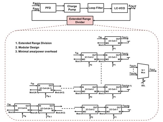
  • An extended range division is achieved using conventional blocks;
  • The modular nature of the proposed approach makes the layout compact, thereby minimizing the area overhead;
  • The digital divider design of the MMD up to sub-10 GHz reduces the power overhead.
The only limitation of the proposed work is excess loading on the input of the divider, which limits the maximum operating frequency. This work presents an extended-range MMD approach built using conventional MMD blocks. Section 2 presents the conventional feedback divider techniques. A brief overview of extended-range MMDs are presented in Section 3. The proposed ER-MMD structure and operation are discussed in Section 4. As a proof of concept, a design example of L 5 / S band PLL using the proposed ER-MMD is studied in Section 5, where dual band PLL is briefly discussed. The measurement results and performance comparison validates the proposed ER-MMD operation in Section 6, followed by the conclusion.

2. Feedback Divider in PLL: An Overview

The majority of prior programmable frequency divider structures are based on programmable counters and 2/3-dividers [10,14]. These two well-known programmable frequency divider architectures are covered in this part, along with some cutting-edge methods for enhancing speed, phase noise, and modulus range.

2.1. Programmable Counter Based Divider

Figure 1a illustrates the design and working of the programmable counter-based divider. It is made up of a programmable counter (PC), a programmable swallow counter (SC), and a dual-modulus prescaler (DMP). When the modulus control signal (MC), which is produced by the programmable swallow counter, is 0 and 1, the D M P O U T is configured to be N and ( N 1 ) , respectively. The timing diagram of the pulse-swallow counter is shown in Figure 1b. A prominent MMD structure is shown in Figure 1c. The operation of a pulse-swallow counter is as follows.
  • The value of PC (P) is always greater than SC (S);
  • Initially, M C is high and both P C and S C start counting in ( N 1 ) mode;
  • As P > S, first S C reaches end-of-count (EOC) and changes M C from high to low;
  • The remaining ( P S ) cycles are counted in N mode.
The frequency division ratio N D I V is thus determined by (1).
N D I V = S · ( N 1 ) + ( P S ) · N = S + N · P
The flowchart depicting the operation of the programmable counter-based divider is given in Figure 2. It should be noted that three variables define the division ratio, N. As a result, the modulus range of the programmable swallow-counter-based dividers is quite broad. However, the DMP directly drives two counters, which increases the output load capacitance for the DMP and impairs high-speed functioning. On the other hand, the two counters continue to operate, increasing power usage. In order to conserve energy, a programmable divider based on a single programmable counter acting as both an SC and a PC was published in [15]. A sub-integer-based clocked divider is presented in [16]. By implementing a modified EOC generation mechanism that relaxes the timing requirement, the speed of the programmable counter has been increased [17].

2.2. Multi Modulus Divider Topologies

A standard MMD is depicted in Figure 1c and features an input ( I N ) and an output ( O U T ). The division ratio is controlled by modulus control ( M I ) and programming pin ( P i , where i = 0 to N). Depending upon the choice of M I and P i , an appropriate modulus out ( M O ) is generated, which acts as M I to the next stage. For logic high values of M I and P i , a divide-by-3 output is generated. Independent of what P i is, the 2 / 3 cell operates in a divide-by-2 mode when M I is logic low. Table 1 summarizes the operation of a standalone 2 / 3 MMD cell. By adding multiple 2 / 3 cells, the division ratio can be increased. In such a scenario, the M I of the final 2 / 3 stage is connected to the supply ( V D D ).
When the required division ratio of a PLL band falls outside the MMD range, this structure does not work. The MMD division range is expressed as in (2),
N = 2 0 P 0 + 2 1 P 1 + 2 2 P 2 + + 2 n P n
where n is the total number of 2 / 3 divider cells (n = 0, 1, 2, so on) and P i , where i = 0 to n, is the 2 / 3 cell digital control. Hence, the conventional MMD division range is limited to 2 n to 2 n + 1 1 . For instance, the division range for a 5-stage MMD is between 32 and 63.

3. Extended Range Divider Topologies

In order to extend the division range, a programmable chain of 2 / 1 frequency dividers was proposed in [18]. This achieves a full division range of 1 to 256 using an 8-stage divider. The 2 / 3 cell is built using conventional logic gates and D-flip–flops [12,19,20]. The power and delay are further optimized when the 2 / 3 cell is designed by low-leakage true single-phase clock (TSPC) flip–flops [21].
A straightforward dual-modulus divider was initially used to replace the P S counter, as shown in Figure 3a. Each cell’s division is set to either 2 or 3, and many such 2 / 3 divider cells are placed to meet the required division range. When the control signal P = 0 , the cell divides by 2, and when the control signal P = 1 then the cell divides by 3. To overcome this limitation, the structure in Figure 3b was proposed (discussed in Section 2.2). According to [12], an OR-gate was used to deactivate the final stage of an MMD, further extending the division range, as shown in Figure 3c. However, this structure does not work when the divider division is varying dynamically, as in the fractional-N PLL. The fractional operation might not succeed due to the inactive stage. This issue was addressed in [13], where the seamless division was accomplished by incorporating additional control logic into the traditional MMD (Figure 3d). The output of the intermediate stages is passed through to a multiplexer (MUX) to increase the divider modulus range, which distorts the MMD’s modular design. The frequency range is enlarged in [22] by adding the logic of [12] to each 2 / 3 cell, which optimizes the first 2 / 3 -cell, which works at the maximum frequency. Each of the aforementioned structures modifies the modular design of MMD and complicates the structure.

4. Proposed Extended Range MMD Structure

In Figure 4, the block diagram of the proposed extended range MMD is displayed. There are N sets of MMDs, each one generating a unique division range. The first set has only one 2 / 3 cell. The second set has two 2 / 3 cells providing a frequency division from 4 to 7. The number of sets can be increased depending on the logic in which the 2 / 3 cell is implemented. All MMD set outputs are fed to a MUX, and the required output is then delivered as a feedback signal to the phase frequency detector (PFD). The working of the proposed ER-MMD is as follows: The PLL output is given as input to all sets of the MMD. The output of each set is given to an input of an MUX. The output of the MUX can provide an extended range division ranging from 2 to 2 N 1 , where N is the number of 2 / 3 cells in the last MMD set. The D-flip–flop of the 2 / 3 cell can be implemented using different logic. Each type of logic has its own set of requirements and provides certain pros and cons.

4.1. D-flip–flop Structures for Divider

High-frequency division is accomplished with an analog frequency divider, which consumes more power but does not require rail-to-rail input signal swing. Figure 5a depicts the divide-by-2 cell and D-latches implemented using current mode logic (CML). Each D-latch is made up of a cross-coupled pair that is connected in a positive feedback arrangement to create negative transconductance and maximize operating frequency. One clock is utilized to drive each D-latch with complimentary clock phases, one of which is used for the flipping circuit and the other for the latching circuit. When C L K is high, M 5 switches O N . The differential pair ( M 1 , 2 ) compares the input amplitudes at the gate terminals and transfers the result to the output nodes. When C L K is low, M 6 switches O N , and the output is held by the regenerative pair transistors ( M 3 , 4 ). Because M 1 , 2 controls how quickly input amplitudes are sensed and transported to the output nodes, they determine the maximum operating frequency.
In a digital frequency divider, the input clock must have a nearly rail-to-rail voltage swing in order to achieve proper frequency division. The divider based on a true single-phase clock (TSPC) D-type flip–flop shown in Figure 5b is based on dynamic logic. It has nine transistors and only uses a single clock. There are two modes in TSPC flip–flop operation: hold mode and evaluation mode. During hold mode, C L K is low, making node X pre-charge to a value based on the input D and node Y to pre-charge to V D D . The output Q B is floating as transistors M 3 and M 7 are O F F . In the evaluation mode, C L K is high. If node X is pre-charged to V D D during hold mode, node Y is discharged, causing Q B to be pulled up by transistor M 3 . If node X is pre-charged to 0 during the hold mode then node Y is not discharged and Q B is pulled down by transistors M 7 and M 10 . The operation frequency can be higher than the static logic divider due to the low transistor count and short input-to-output delay. The MMD can operate until sub-10 GHz, depending upon the technology.
Another structure that uses dynamic logic is the extended true single phase clocking (E-TSPC)-based D-flip–flop. This is realized by using 6 transistors, as shown in Figure 5c, thereby reducing the critical path, which in turn enhances the operating frequency. The operation of an E-TSPC flip–flop is discussed in detail in [23]. The propagation delay and power consumption analysis are presented in [24]. Because of the static current and noise immunity issues, the E-TSPC circuit needs special care during its design. They are suitable for low-supply voltage and low-power applications. The frequency of operation is better than the TSPC-based D-flip–flop. The overall performance comparison of all three structures is tabulated in Table 2. Depending upon the target frequency, power requirement, and output phases, one can choose the suitable D-flip–flop logic.

4.2. Circuit Implementation

In this work, the 2 / 3 cells are implemented using TSPC logic. The combinational logic, except for an inverter, is incorporated inside the flop to lessen propagation delay and current consumption [25]. The TSPC flop structure is shown in Figure 6. The flop is built as a single circuit that includes the conventional D-flip–flop, A N D gate, and O R gate. The main advantage of this structure is that it requires only single input and produces peak-to-peak output, because of which the intermediate buffer stages are not required. The ER-MMD design is simulated in UMC 65-nm CMOS. The TSPC-based MMD works up to 6-GHz across process, voltage, and temperature (PVT). This means a maximum of eight 2 / 3 MMD sets can be incorporated, proving a division range from 2 to 511.
The current consumption, rise time, and fall time of the ER-MMD are summarized for three process corners, viz., slow–slow (SS), fast–fast (FF), and typical–typical (TT). For each of the three process corners the current consumption, rise time, and fall time of the MMD output was simulated for three temperatures, viz., 40 , 27 , and 85 , and three voltages, viz., 0.9 V, 1 V, and 1.1 V, which is actually ± 10 % supply voltage variation.
The first 2 / 3 cell is the most power-consuming block. Figure 7 shows the current consumption of the proposed ER-MMD, which ranges from 370 μ A to 610 μ A across PVT. The rise time and fall time ( 10 % to 90 % of supply) of the proposed ER-MMD output at 6-GHz input across PVT is shown in Figure 8 and Figure 9, respectively. Even though the maximum variation in the rise and fall time across PVT is 1.5 ps and 1 ps, respectively, the proposed ER-MMD produces the desired output. This approach can extend the maximum division ratio from 511 to 1023 using E-TSPC logic in the first few stages and further using CML logic. Even though the ER-MMD designed using CML logic comes at a cost of very high power and stringent layout complexities, the CML logic is preferred for a PLL designed to work at m m -wave frequencies.
The limitation of this structure is the extra loading on the input. At high frequencies, this constraint is very critical. The parasitic capacitance ( C p a r ) at the input of the first 2 / 3 cell when supply is O N and O F F are tabulated in Table 3.
A 20 % reduction in C p a r is observed when the 2 / 3 cell is O F F . From this observation, one way to reduce the extra loading is to power O N only one 2 / 3 set at a time. The total C p a r when all sets are O N and only one set is O N is tabulated in Table 3. Thus, the extra C p a r added in the proposed ER-MMD compared to a conventional MMD is reduced from 8 times to 6.4 times. This is the reason for ER-MMD to operate only up to 6 GHz using TSPC logic. There is no work in the literature that analyzes the effect of loading on the frequency of operation. The extension of this work would be to build an extended range MMD with minimal loading while maintaining the modular structure of the 2 / 3 cell.

5. Design of L5/S Band Dual VCO PLL

The work published in [26] is briefly discussed as proof of concept. Figure 10 shows a comprehensive block diagram of PLL. A pre-divider of 5 divides the crystal frequency of 26 MHz to 5.2 MHz ( f R E F ), which is enough to accomplish both L 5 and S bands while the PLL is in integer mode. The PLL loop dynamics are chosen to ensure acceptable loop bandwidth and stability. The typical PFD, charge pump (CP), and a second-order loop filter are employed. The lower PLL loop bandwidth is supported by a nominal settling time for improved far-out PN.
The PLL loop bandwidth is chosen to be less than f R E F / 20 . To lessen the current mismatch, an off-chip low drop-out regulator (LDO) supplies the CP current ( I C P ). For PLL stability, a phase margin of 49° and above is maintained over the complete frequency range. Using the loop parameters ( f R E F , feedback division ratio, I C P , and VCO gain), passive loop filter (second order) values are chosen. A C 1 of 150 pF, C 2 of 15 pF, and R 1 of 50 K Ω , (see Figure 10) accomplishes phase margin of 54° and 49°, maintaining a loop bandwidth of 97 KHz and 140 KHz for S-band and L 5 -band, respectively.
In Figure 11, the block diagram of the ER-MMD is depicted, which is a sub-set of the ER-MMD shown in Figure 4. There are two sets of MMDs used, one with 5-stage TSPC 2 / 3 cells and the other with 6-stage cells. Both sets receive the divide-by-4 output of the VCO as input. Both MMD set outputs are fed into a simple MUX, and the desired output is then delivered as a feedback signal to the PFD. Table 4 illustrates how the proposed ER-MMD functions. MMD with six stages is operational when S E L is high. When the input control bits P[5:0] is used, an output in the range of f i n / 64 to f i n / 127 is produced. MMD with five stages is operational when S E L is low. An output between f i n / 32 to f i n / 63 is produced when control bits P[4:0] are prfovided as inputs.
The proposed ER-MMD has minimal additional die area. The ER-MMD has a negligible power overhead because it operates at a sub-GHz frequency. For both sets of MMDs, the control signals P 0 to P 4 are utilized. As a result, the goal of adopting a conventional design and creating an ER-MMD functioning from 32 to 127 is realized with low area and power overhead.

5.1. VCO, CML Divider, and MUX

A differential LC-VCO that runs at double the intended local oscillator (LO) frequencies is employed. The I/Q LO signals are produced using a divide-by-2 CML device. The desired band is chosen at the output using the CML MUX. The operating frequencies of the VCO for the L 5 -band are 2.2 2.4 GHz, and for the S-bands are 4.7 5.2 GHz. Table 5 provides an overview of both VCOs frequency and PN. The divide-by-4 receives the output of the MUX as input before sending it to the MMD.
A complementary cross-coupled LC-VCO is used in this PLL. For discrete tuning, a binary weighted, 4-bit switched capacitor array (SCA) is incorporated. Two varactors biased at different bias voltages are designed for fine-tuning with good linearity [27]. The quality factor (Q) for both VCO across the frequency range is maintained above 10 by sizing them appropriately. The CML MUX output is routed to I/O pads via a 50 Ω driver.

5.2. PFD, CP, and Loop Filter

The PLL PN, especially the in-band PN, rest on the non-linearity of PFD and CP. In this work, PFD based on conventional D-flip–flop is used. An appropriate delay is added in the reset path to overcome the dead-zone issue [28]. The CP implementation is based on the switch-to-drain architecture [28]. The CP current is fixed at 0.35 mA and avoids programmability. Thus, the current is provided using an off-chip LDO in order to minimize the ripple on V t u n e . The loop parameters are chosen carefully due to the lack of CP programmability. A single loop filter is utilized for both LC-VCOs.

6. Measurement Results

A narrow-band dual-VCO PLL was fabricated using the UMC 65-nm CMOS process. When powered using a 1 V supply, the PLL consumes 7.9 mW in the L 5 -band and 6.4 mW in the S-band. The PLL core size is 1.4 mm 2 (ref. Figure 12). The area of the proposed ER-MMD is 300 μ m × 20 μ m, as shown in Figure 12, which is negligible compared to the overall chip area. Due to two on-chip passive inductors, the large chip area is understandable. Even with ER-MMD of Figure 4, the chip overhead is minimal. The two inductors are positioned as far apart as feasible and are adequately insulated to prevent any coupling between them. The test board is mounted with a 68-pin QFN package die. An LDO installed on the test board supplies the 1.0 V supply. An Agilent EXA N9010A signal-analyzer is used for PN measurement.
For the L 5 -band, an MMD set with 5 stage TSPC 2 / 3 cells is active. A division ratio of 57 is selected, which produces 5.2 MHz divider output. The PN of LO measured at the L 5 -band is shown in Figure 13. The PLL attains the PN of 49.44 dBc/Hz, 95.63 dBc/Hz, and 121.25 dBc/Hz at 10 KHz, 100 KHz, and 1 MHz offset, respectively. For S-band, MMD set with 6 stage TSPC 2 / 3 cells is active. A division ratio of 120 is selected which produces 5.2 MHz divider output. The PN of LO measured at the S-band is shown in Figure 14. The PLL attains the PN of 57.42 dBc/Hz, 94.56 dBc/Hz, and 120.12 dBc/Hz at 10 KHz, 100 KHz, and 1 MHz offset, respectively. The phase noise results prove the dual VCO L 5 / S band PLL, and thereby the proposed ER-MMD structure is working.
Table 6 compares the proposed ER-MMD with recent techniques. The work in [29] provides a 1 to 256 division ratio and also produces 50 % duty cycle, but consumes higher power. The maximum operating frequency of the work in [5] is half of the proposed structure. Although the maximum frequency in [6] is a little high, the division ratio provided is limited.

7. Conclusions

A multiplexer-based ER-MMD approach is presented for multi-band PLLs. Conventional feedback divider techniques are discussed. Previous extended-range MMD architectures are examined. The design details of the proposed ER-MMD are given. The 2 / 3 cell is implemented in TSPC logic. Another logic implementation such as CML and E-TSPC is also examined, summarizing the pros and cons of each logic. As a proof of concept, a dual VCO L 5 / S band integer-N PLL is designed in UMC 65-nm CMOS, incorporating the proposed ER-MMD with 32 to 127 division ratio. The performance comparison shows that the proposed ER-MMD has better supply efficiency, maintaining the modular structure and minimal area overhead.

Author Contributions

Circuit idea, R.S.P.; circuit design/layout, R.S.P.; on-wafer testing, R.S.P.; writing—original draft preparation, R.S.P., A.D. and B.D.S.; writing—review and editing, R.S.P., A.D. and B.D.S. All authors have read and agreed to the published version of the manuscript.

Funding

This research is funded by SAMEER Kolkata, India.

Data Availability Statement

Data is contained within the article. The data presented in this study are available in [26].

Conflicts of Interest

The authors declare no conflict of interest.

References

  1. Datta, A.K.; Patel, R. CPU Scheduling for Power/Energy Management on Multicore Processors Using Cache Miss and Context Switch Data. IEEE Trans. Parallel Distrib. Syst. 2013, 25, 1190–1199. [Google Scholar] [CrossRef]
  2. Xing, Y.; Liu, F.; Xiao, N.; Chen, Z.; Lu, Y. Capability for Multi-Core and Many-Core Memory Systems: A Case-Study with Xeon Processors. IEEE Access 2019, 7, 47655–47662. [Google Scholar] [CrossRef]
  3. Available online: https://www.analog.com/en/products/adf4355-2.html (accessed on 31 January 2022).
  4. Available online: https://www.st.com/resource/en/datasheet/stw81200.pdf (accessed on 31 January 2022).
  5. El Alaoui Ismaili, Z.; Ismaili, A.; Ajib, W.; Gagnon, F.; Nabki, F. A 0.13 μm CMOS fully integrated 0.1 to 12 GHz frequency synthesizer for avionic SDR applications. In Proceedings of the IEEE International Symposium on Circuits and Systems (ISCAS) 2017, Baltimore, MD, USA, 28–31 May 2017; pp. 1–4. [Google Scholar]
  6. Kim, N.-S.; Rabaey, J.M. A 3–10 mW, 3.1–10.6 GHz integer-N QPLL with reference spur reduction technique for UWB-based cognitive radios. In Proceedings of the IEEE Radio Frequency Integrated Circuits Symposium, Phoenix, AZ, USA, 17–19 May 2015; pp. 67–70. [Google Scholar]
  7. Yu, S.-A.; Kinget, P. A 0.65-V 2.5-GHz Fractional-N Synthesizer with Two-Point 2-Mb/s GFSK Data Modulation. IEEE J. Solid-State Circuits 2009, 44, 411–2425. [Google Scholar] [CrossRef]
  8. Ko, J.; Kim, J.; Cho, S.; Lee, K. A 19-mW 2.6-mm/sup 2/ L1/L2 dual-band CMOS GPS receiver. IEEE J. Solid-State Circuits 2005, 40, 1414–1425. [Google Scholar]
  9. Li, S.; Li, J.; Gu, X.; Wang, H.; Li, C.; Wu, J.; Ta, M. Reconfigurable All-Band RF CMOS Transceiver for GPS/GLONASS/Galileo/Beidou with Digitally Assisted Calibration. IEEE Trans. Very Large Scale Integr. Syst. 2015, 23, 1814–1827. [Google Scholar] [CrossRef]
  10. Razavi, B. RF Microelectronics, 2nd ed.; Prentice-Hall: Upper Saddle River, NJ, USA, 2011. [Google Scholar]
  11. Vaucher, C.; Kasperkovitz, D. A wide-band tuning system for fully integrated satellite receivers. IEEE J. Solid-State Circuits 1998, 33, 987–997. [Google Scholar] [CrossRef]
  12. Vaucher, C.S.; Ferencic, I.; Locher, M.; Sedvallson, S.; Voegeli, U.; Wang, Z. A family of low-power truly modular programmable dividers in standard 0.35-/spl mu/m CMOS technology. IEEE J. Solid-State Circuits 2000, 35, 1039–1045. [Google Scholar] [CrossRef]
  13. Elkholy, A.; Saxena, S.; Nandwana, R.K.; Elshazly, A. A 2.0–5.5 GHz Wide Bandwidth Ring-Based Digital Fractional-N PLL With Extended Range Multi-Modulus Divider. IEEE J. Solid-State Circuits 2016, 51, 1771–1784. [Google Scholar] [CrossRef]
  14. Gundla, A.R.; Chen, T. A low power frequency synthesizer for biosensor applications in the MedRadio band. In Proceedings of the IEEE International Midwest Symposium on Circuits and Systems, Lisbon, Portugal, 24–27 October 2015; pp. 1–4. [Google Scholar]
  15. Kim, K.-Y.; Min, Y.-J.; Kim, S.-W.; Park, J. Low-power programmable divider with a shared counter for frequency synthesiser. IET Circuits Devices Syst. 2011, 5, 170–176. [Google Scholar] [CrossRef]
  16. Gangasani, G.R.; Kinget, P.R. A 0.5 V, 9-GHz Sub-Integer Frequency Synthesizer Using Multi-Phase Injection-Locked Prescaler for Phase-Switching-Based Programmable Division with Automatic Injection-Lock Calibration in 45-nm CMOS. IEEE Trans. Circuits Syst. II Express Briefs 2019, 66, 803–807. [Google Scholar] [CrossRef]
  17. Som, I.; Sarangi, S.; Bhattacharyya, T.K. A 7.1-GHz 0.7-mW Programmable Counter with Fast EOC Generation in 65-nm CMOS. IEEE Trans. Circuits Syst. II Express Briefs 2020, 67, 2397–2401. [Google Scholar] [CrossRef]
  18. Lin, C.-S.; Chien, H.; Wey, C. A 5.5-GHz 1-mW Full-Modulus-Range Programmable Frequency Divider in 90-nm CMOS Process. IEEE Trans. Circuits Syst. II Express Briefs 2011, 58, 550–554. [Google Scholar] [CrossRef]
  19. Ergintav, A.; Herzel, F.; Borngraeber, J.; Ng, H.J.; Kissinger, D. Low-power and low-noise programmable frequency dividers in a 130 nm SiGe BiCMOS technology. In Proceedings of the IEEE 15th International New Circuits and Systems Conference (NEWCAS), Strasbourg, France, 25–28 June 2017; pp. 105–108. [Google Scholar]
  20. Ergintav, A.; Herzel, F.; Fischer, G.; Kissinger, D. A Study of Phase Noise and Frequency Error of a Fractional-N PLL in the Course of FMCW Chirp Generation. IEEE Trans. Circuits Syst. I Regul. Pap. 2019, 66, 1670–1680. [Google Scholar] [CrossRef]
  21. Kim, N.-S.; Rabaey, J.M. A 3.1–10.6-GHz 57-Bands CMOS Frequency Synthesizer for UWB-Based Cognitive Radios. IEEE Trans. Microw. Theory Tech. 2018, 66, 4134–4146. [Google Scholar] [CrossRef]
  22. Kulkarni, P.; Garg, S.; Agrawal, S.; Baghini, M.S. Low Power Extended Range Multi-Modulus Divider Using True-Single-Phase-Clock Logic. In Proceedings of the IEEE 34th International Conference on VLSI Design (VLSID), Virtual, 20–24 April 2021; pp. 99–104. [Google Scholar]
  23. Soares, J.N.; Van Noije, W.A.M. A 1.6-GHz dual modulus prescaler using the extended true-single-phase-clock CMOS circuit technique (E-TSPC). IEEE J. Solid-State Circuits 1999, 34, 97–102. [Google Scholar] [CrossRef] [Green Version]
  24. Yu, X.P.; Do, M.A.; Lim, W.M.; Yeo, K.S.; Ma, J.-G. Design and Optimization of the Extended True Single-Phase Clock-Based Prescaler. IEEE Trans. Microw. Theory Tech. 2006, 54, 3828–3835. [Google Scholar] [CrossRef]
  25. Kathiah, S.; Aniruddhan, S. Replica bias scheme for efficient power utilization in high-frequency CMOS digital circuits. In Proceedings of the IEEE International Symposium on Circuits and Systems (ISCAS), Victoria, Australia, 1–5 June 2014; pp. 1002–1005. [Google Scholar]
  26. Peerla, R.S.; Chary, P.; Dutta, A.; Sahoo, B.D. A Dual VCO Based L5/S Band PLL with Extended Range Divider for IRNSS Application. In Proceedings of the IEEE International Symposium on Circuits and Systems (ISCAS), Austin, TX, USA, 28 May–1 June 2022; pp. 1699–1703. [Google Scholar]
  27. Jin, J.; Yu, X.; Liu, X.; Lim, W.M.; Zhou, J. A wideband voltage-controlled oscillator with gain linearized varactor bank. IEEE Trans. Components Packag. Manuf. Tech. 2014, 4, 905–910. [Google Scholar] [CrossRef]
  28. Razavi, B. Design of CMOS Phase-Locked Loops: From Circuit Level to Architecture Level; Cambridge University Press: Cambridge, UK, 2020. [Google Scholar]
  29. Wang, Y.; Wang, Y.; Wu, Z.; Quan, Z.; Liou, J.J. A Programmable Frequency Divider with a Full Modulus Range and 50% Output Duty Cycle. IEEE Access 2020, 8, 102032–102039. [Google Scholar] [CrossRef]
Figure 1. (a) Block diagram of conventional pulse-swallow-based feedback divider, (b) timing diagram showing the operation of a pulse-swallow counter, and (c) block diagram of conventional 2 / 3 cell-based MMD structure.
Jlpea 13 00043 g001
Figure 2. Flowchart showing the working principle of the pulse-swallow feedback divider.
Jlpea 13 00043 g002
Figure 3. Block diagram depicting structures of (a) dual modulus divider, (b) prominently used MMD, (c) extended range MMD implemented in [12], and (d) the extended range MMD proposed in [13].
Jlpea 13 00043 g003
Figure 4. Block diagram of the proposed multiplexer-based ER-MMD.
Jlpea 13 00043 g004
Figure 5. Block diagram of (a) CML divide-by-2 and basic circuit implementation of D-flip–flop, (b) simple TSPC logic-based D-flip–flop circuit, and (c) extended TSPC (E-TSPC)-based D-flip flop circuit.
Jlpea 13 00043 g005
Figure 6. Circuit implementation of TSPC flop [25].
Jlpea 13 00043 g006
Figure 7. Current consumption of the proposed ER-MMD across PVT.
Jlpea 13 00043 g007
Figure 8. Extracted simulation of rise time of ER-MMD output with 6 GHz input across PVT.
Jlpea 13 00043 g008
Figure 9. Extracted simulation of fall time of ER-MMD output with 6 GHz input across PVT.
Jlpea 13 00043 g009
Figure 10. Dual VCO-based L 5 / S -band PLL block diagram designed in [26].
Jlpea 13 00043 g010
Figure 11. Block diagram of the proposed extended range MMD designed in [26].
Jlpea 13 00043 g011
Figure 12. PCB mounted die micrograph of the dual VCO L 5 / S band PLL highlighting the proposed ER-MMD.
Jlpea 13 00043 g012
Figure 13. Measured LO PN at L 5 -band when ER-MMD division ratio is set to 57.
Jlpea 13 00043 g013
Figure 14. Measured LO PN at S-band when ER-MMD division ratio is set to 120.
Jlpea 13 00043 g014
Table 1. Working of standalone 2 / 3 MMD cell.
Input P i MI Output
f i n X0 f i n / 2
f i n 01 f i n / 2
f i n 11 f i n / 3
Table 2. Performance comparison between CML, TSPC, and E-TSPC D-flip–flop.
CMLTSPCE-TSPC
SpeedHighModerateHigh
Input
Swing
LowRail-to-RailRail-to-Rail
Output
Swing
LowRail-to-RailRail-to-Rail
Output
Phases
Diff.Diff./SingleDiff./Single
Input
Clock
Diff.SingleSingle
PowerHighLowModerate
Table 3. Parasitic capacitance impact of first 2 / 3 cell and complete ER-MMD in O N and O F F state.
Single 2/3 CellComplete ER-MMD
ON StateOFF StateAll Sets ONSingle Set ON
C p a r 15 fF12 fF120 fF96 fF
Table 4. Fuctioning of proposed ER-MMD.
L 5 BandS BandDivision Range
MMD control bitsP[4:0]P[5:0]
SEL = 0YesNo32 to 63
SEL = 1NoYes64 to 127
Table 5. Frequency planning, current consumption, and targeted PN for VCOs.
S-Band L 5 -Band
VCO Frequency
(MHz)
4700–52002200–2400
LO Frequency
(MHz)
2350–26001100–1200
Center Frequency
(MHz)
2495.021178.45
Current (mA)3.55
PN @ 1 MHz
(dBc/Hz)
−120−120
PN @ 100 KHz
(dBc/Hz)
−90−90
Table 6. Performance comparison of ER-MMD with recent structures.
This Work [29][5 [6]
Technology (nm)6518013065
Division Ratio2–5111–256128–19224–80
Supply (V)11.81.21
Max. Frequency (GHz)62.336.5
PN at 1 MHz offset
(dBc/Hz)
−155 −140 NA −141
Div. Power (mW)0.53.4NA1
Power Efficiency
(GHz/mW)
120.68NA6.25
50% Output
Duty Cycle
NoYesNoNo
R + C + CC Extracted simulation. Extracted simulation.
Disclaimer/Publisher’s Note: The statements, opinions and data contained in all publications are solely those of the individual author(s) and contributor(s) and not of MDPI and/or the editor(s). MDPI and/or the editor(s) disclaim responsibility for any injury to people or property resulting from any ideas, methods, instructions or products referred to in the content.

