
A Spintronic 2M/7T Computation-in-Memory Cell

Abstract
:1. Introduction
- A novel cell design is proposed based on the conventional 6T-SRAM cell and MTJs. Two binary values can be stored in the proposed cell: one in the SRAM and another in the MTJ parts.
- This proposed cell can operate based on the CiM-A scheme, hence alleviating the scalability and sense margin limitation issues of CiM-P architectures. In addition, it also has the ability to perform CiM-P for aggregation functions. Therefore, it is possible to gain benefits from both the CiM-A and CiM-P types.
- For aggregation functions, our proposed cell can operate as a conventional SRAM as well as a conventional STT-MRAM cell. Therefore, both conventional memory and CiM operations are supported.
- The presence of MTJs enables non-volatile SRAM. It supports storing and restoring the content from SRAM to STT-MRAM and back.
- We perform extensive circuit-level simulations and evaluations to validate the functionality and verify the robustness of the proposed cell design under three-sigma process variation and various operating temperatures.
- The effectiveness of using the proposed CiM for multiple high-level applications is investigated.
2. Background
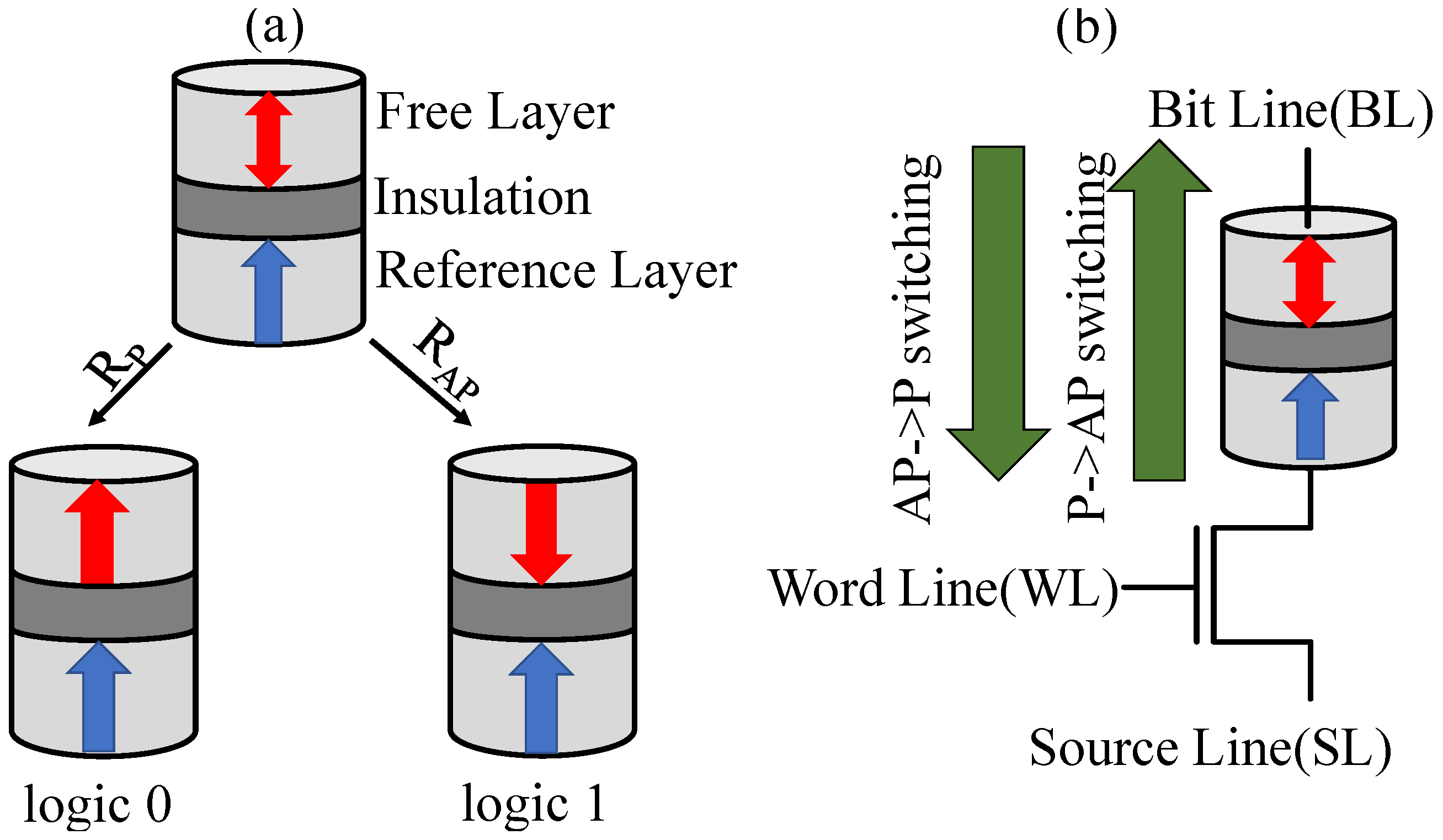
2.1. Spin-Transfer Torque Magnetic RAM
2.2. Motivations and Related Works
2.2.1. Motivation of the Proposed Cell
2.2.2. Related Works
2.2.3. Proposed Cell Compared to Other SRAM-CiM Designs
3. Proposed Cell Design
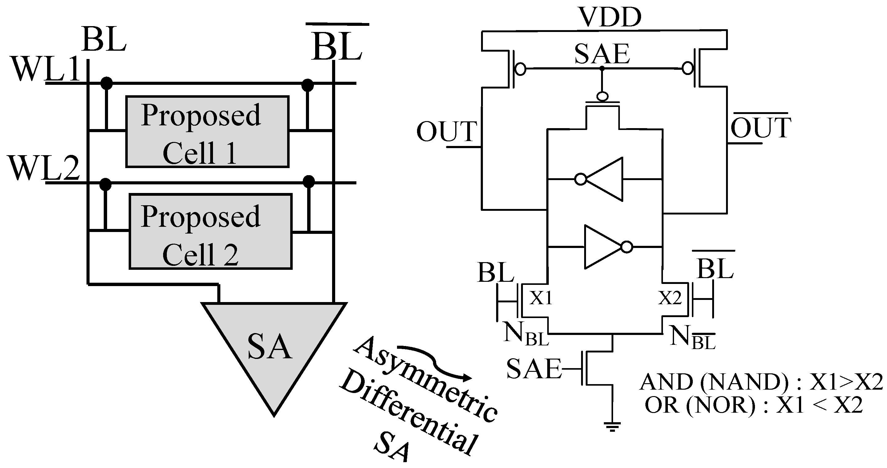
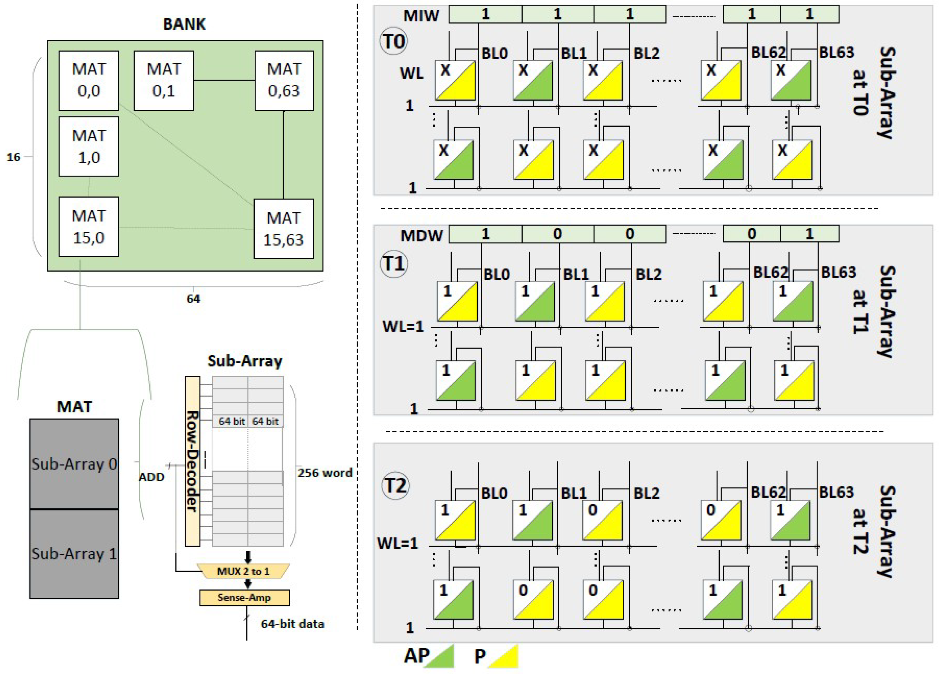
3.1. Overview of the CiM Technique
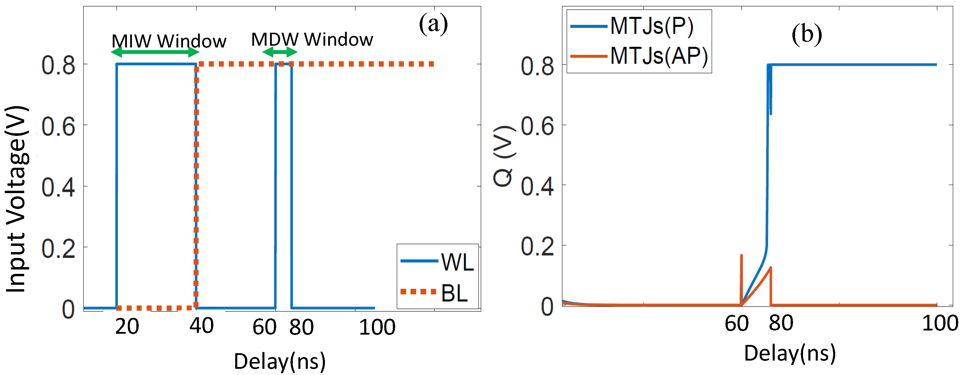
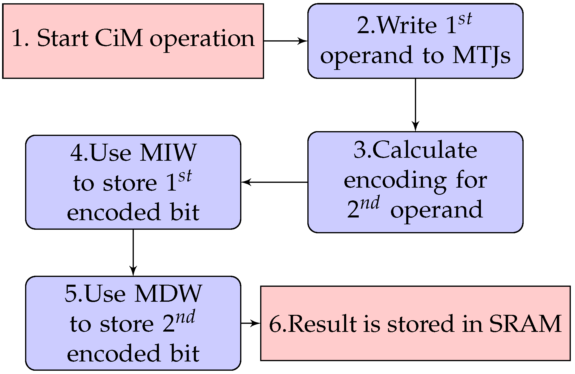
- The long SRAM write is timed in a way that it is independent of the MTJ states. We will denote this operation as the MTJ independent write (MIW) operation.
- The short SRAM write is timed in a way that allows for a successful write operation to the SRAM cell in case the MTJs are in the low-resistance P state. However, the write operation fails if the MTJs are in the high-resistance AP state. This short write operation is therefore dependent on the MTJ state and will be denoted as the MTJ dependent write (MDW) operation.
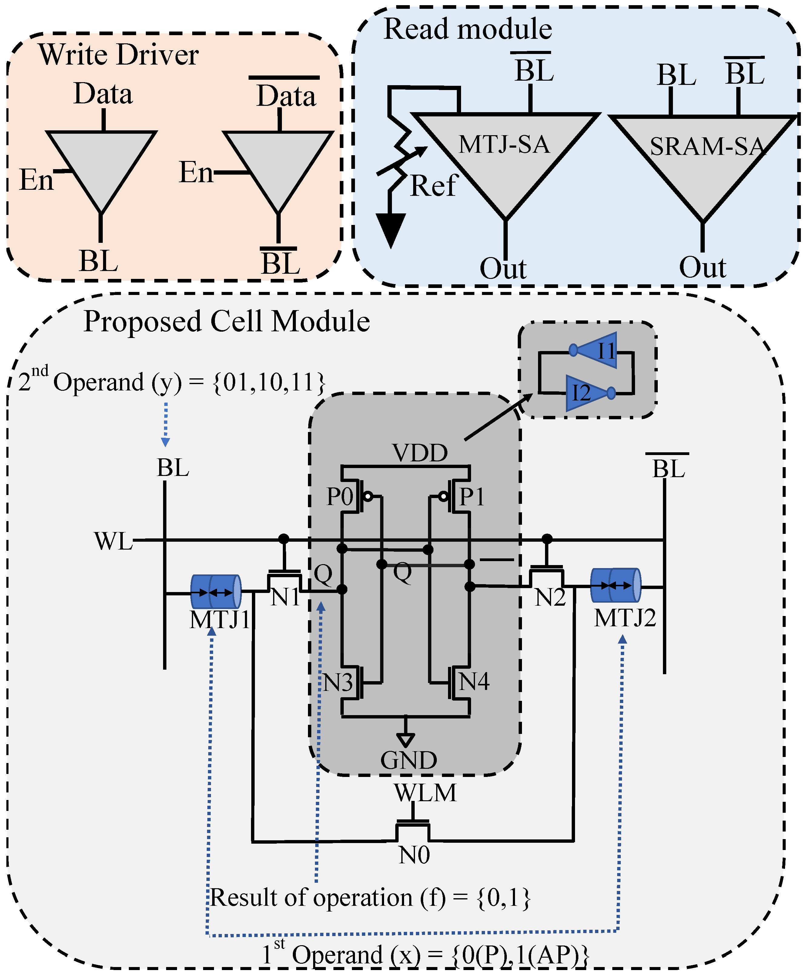
3.2. Circuit-Level Hybrid Cell Design
3.2.1. CiM Operation Principle
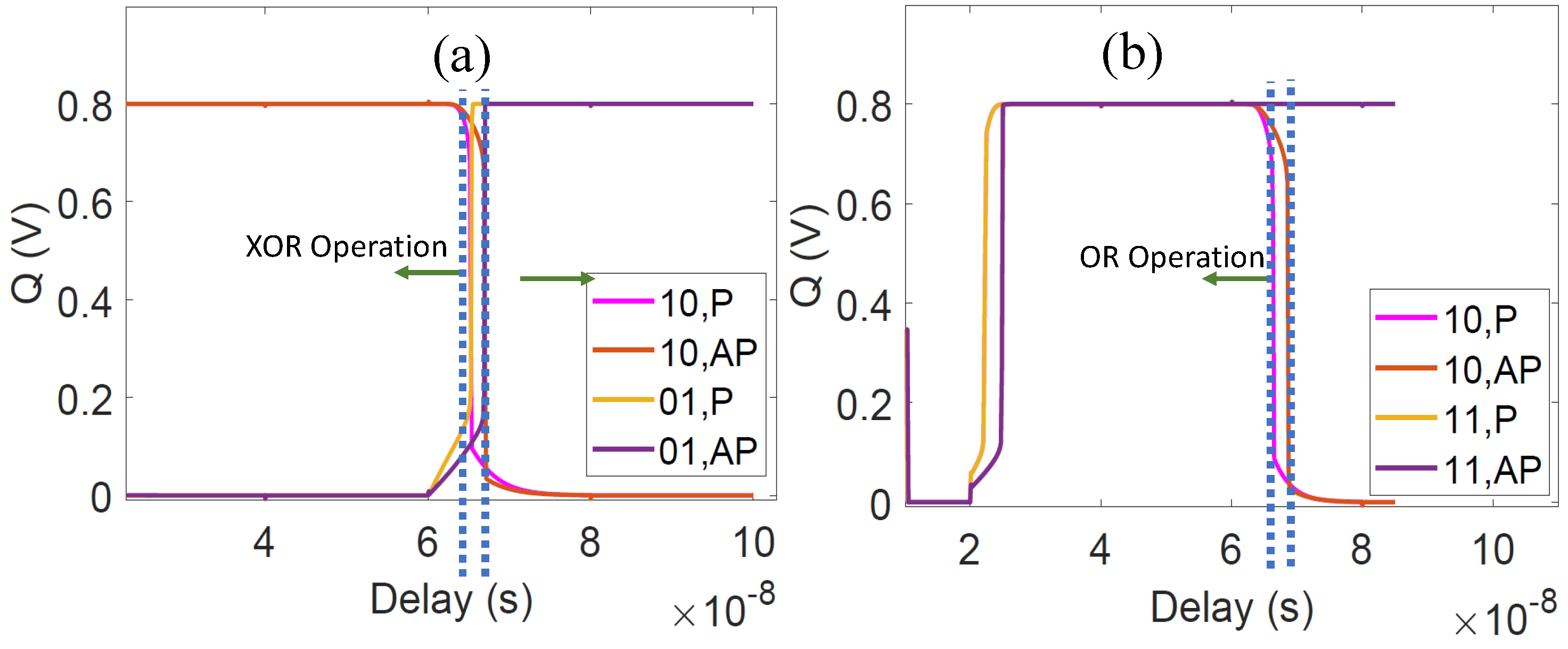
3.2.2. XOR CiM Operation
3.2.3. OR CiM Operation
3.2.4. Implication CiM Operation
3.3. Realization of CiM-P with the Proposed Design
3.4. Conventional Memory Operations
3.4.1. Conventional SRAM Operation
3.4.2. Conventional STT-MRAM
4. Experimental Results and Evaluation
4.1. Simulation Set-Up
4.2. CiM Operation Waveform Results
4.2.1. Operand-Encoding Signals for CiM Operations
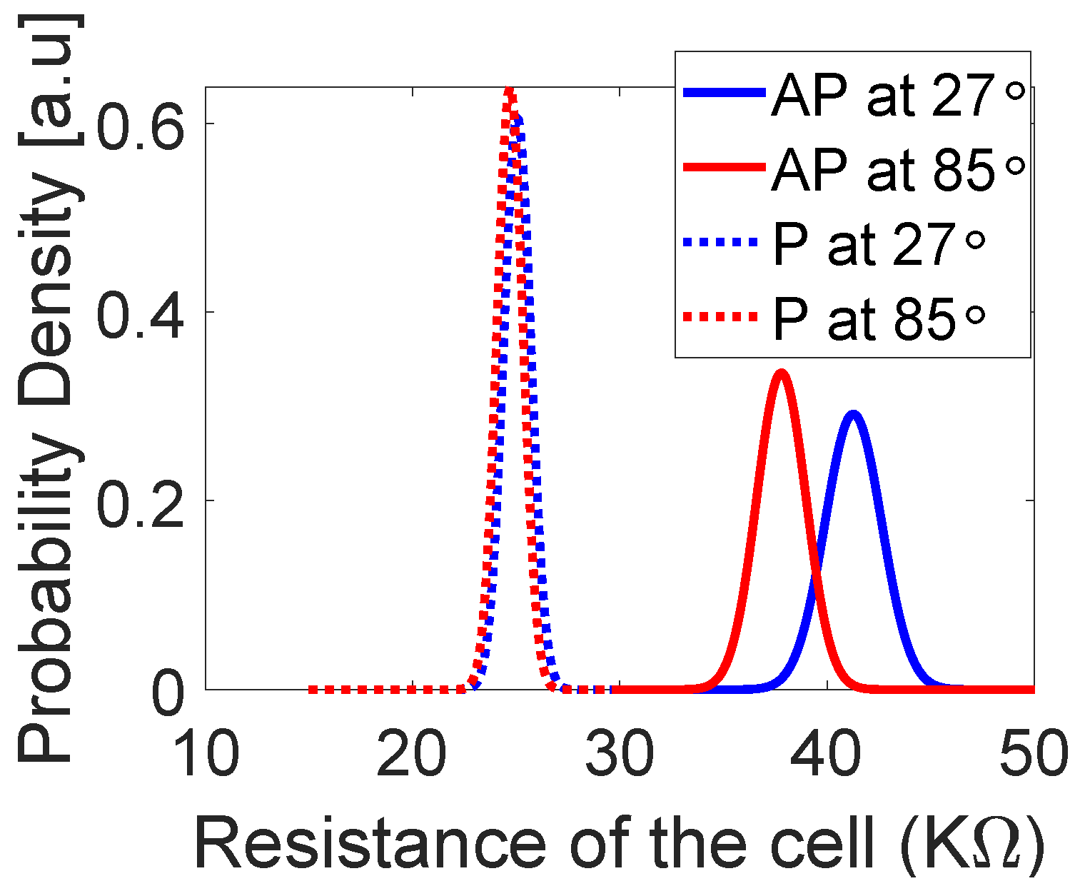
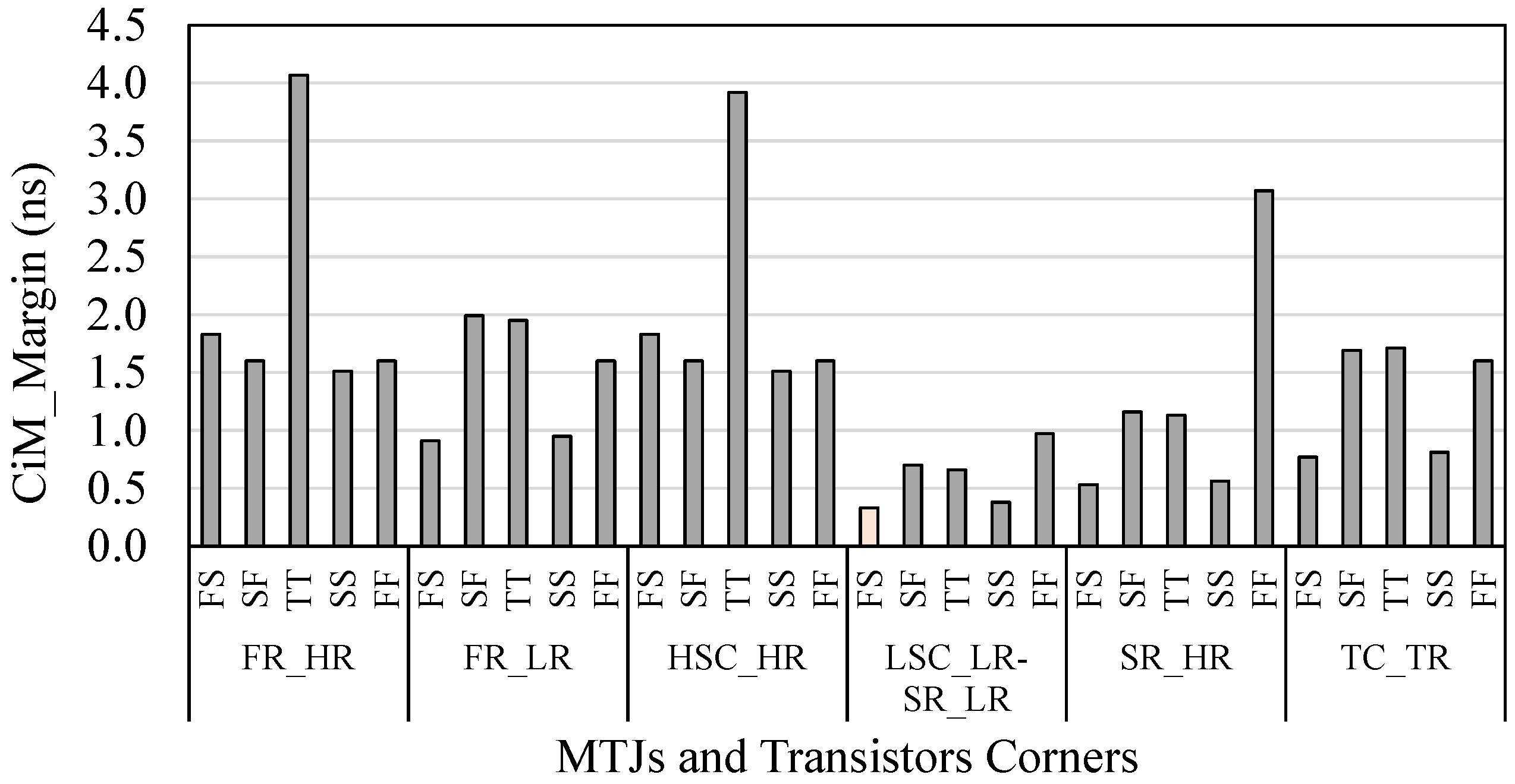
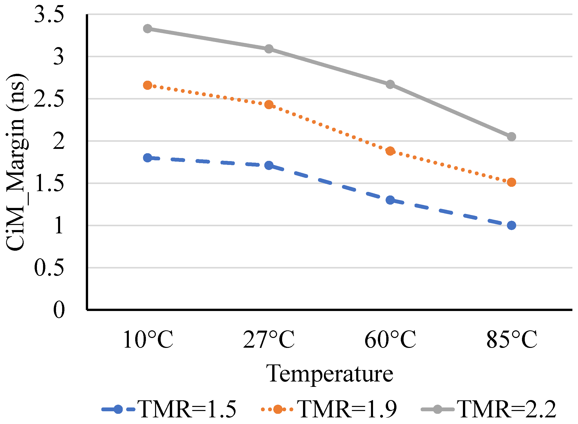
4.2.2. Robustness of CiM Operations under Variations
4.2.3. Impact of Temperature on the
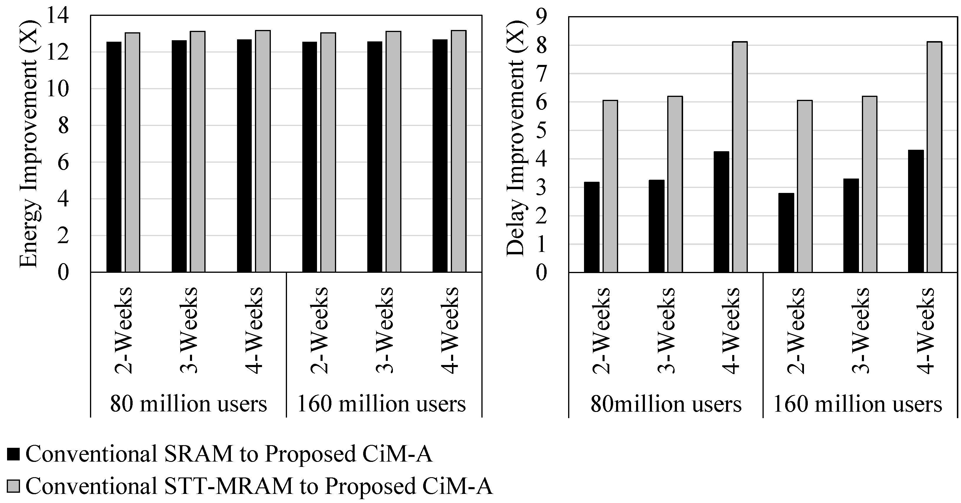
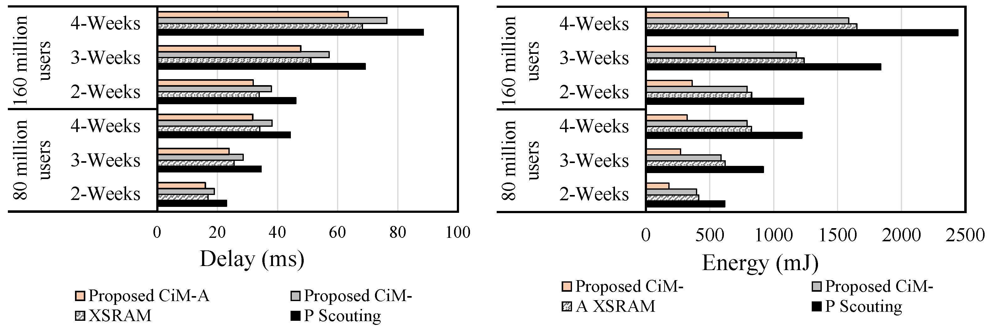
4.3. Figures of Merits
5. Analysis and Comparison to the State of the Art
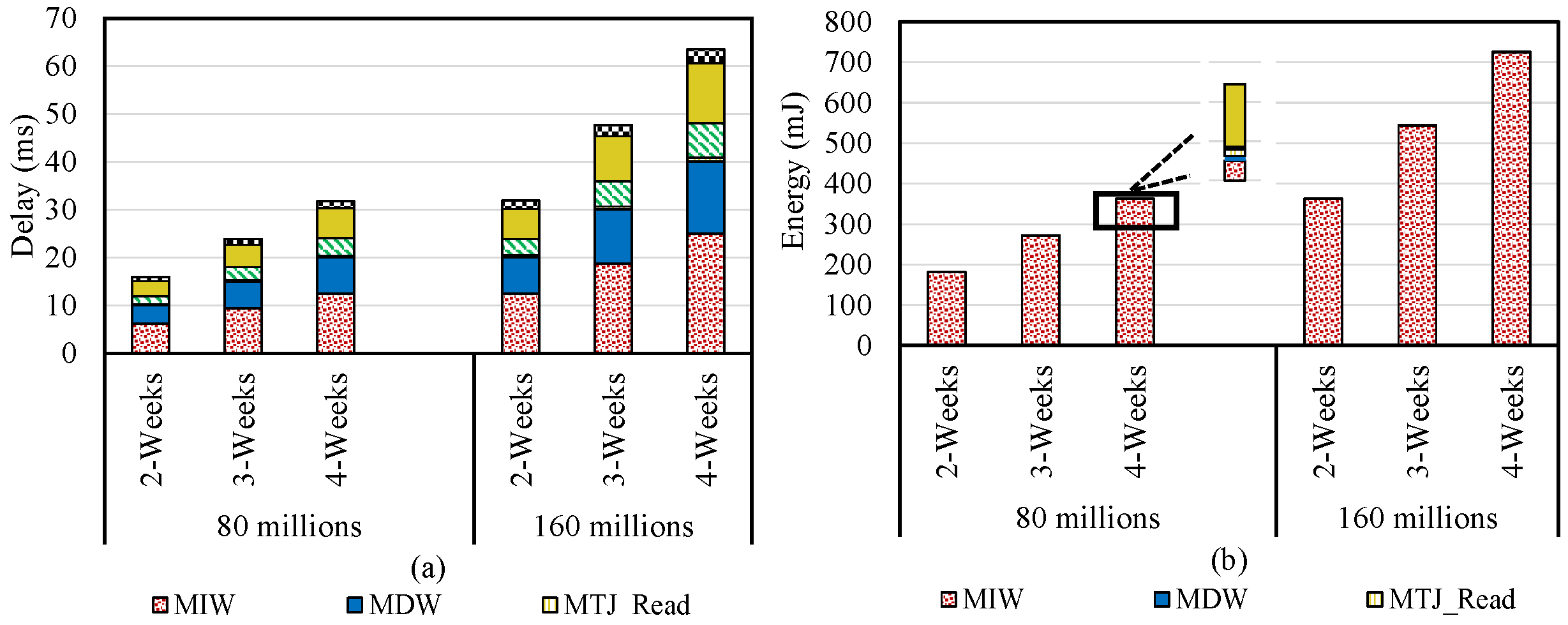
5.1. Database Query
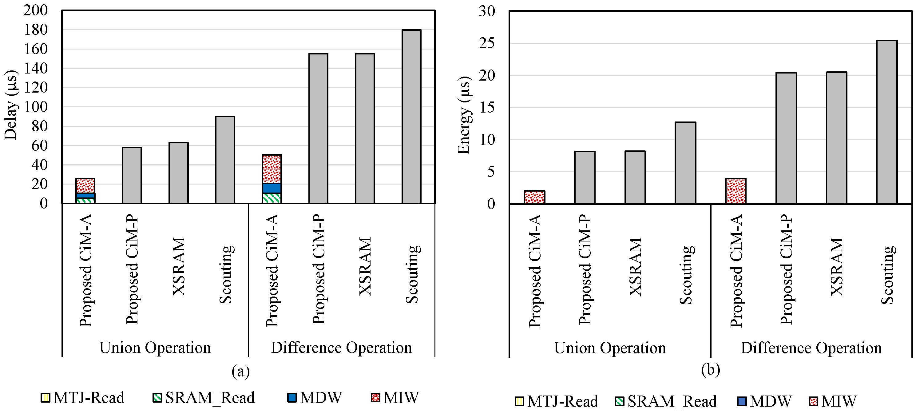
5.2. Bit Vector Set
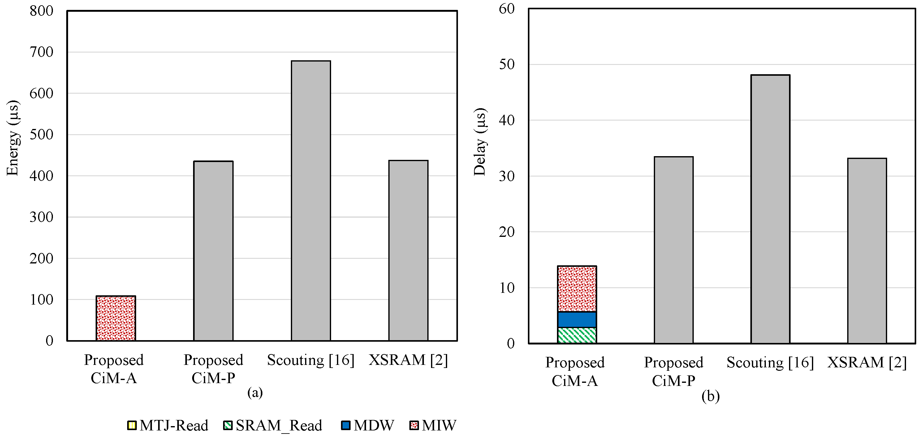
5.3. Pure Bitwise Operation
6. Conclusions
Author Contributions
Funding
Conflicts of Interest
References
- Seshadri, V.; Hsieh, K.; Boroum, A.; Lee, D.; Kozuch, M.A.; Mutlu, O.; Gibbons, P.B.; Mowry, T.C. Fast Bulk Bitwise AND and OR in DRAM. IEEE Comput. Archit. Lett. 2015, 14, 127–131. [Google Scholar] [CrossRef]
- Agrawal, A.; Jaiswal, A.; Lee, C.; Roy, K. X-SRAM: Enabling In-Memory Boolean Computations in CMOS Static Random Access Memories. IEEE Trans. Circuits Syst. I Regul. Pap. 2018, 65, 4219–4232. [Google Scholar] [CrossRef] [Green Version]
- Nair, S.M.; Bishnoi, R.; Vijayan, A.; Tahoori, M.B. Dynamic Faults based Hardware Trojan Design in STT-MRAM. In Proceedings of the 2020 Design, Automation Test in Europe Conference Exhibition (DATE), Grenoble, France, 9–13 March 2020; pp. 933–938. [Google Scholar] [CrossRef]
- Sebastian, A.; Le Gallo, M.; Khaddam-Aljameh, R.; Eleftheriou, E. Memory devices and applications for in-memory computing. Nat. Nanotechnol. 2020, 15, 529–544. [Google Scholar] [CrossRef] [PubMed]
- Li, C.; Hu, M.; Li, Y.; Jiang, H.; Ge, N.; Montgomery, E.; Zhang, J.; Song, W.; Dávila, N.; Graves, C.E.; et al. Analogue signal and image processing with large memristor crossbars. Nat. Electron. 2018, 1, 52–59. [Google Scholar] [CrossRef]
- Khalifa, M.; Ben-Hur, R.; Ronen, R.; Leitersdorf, O.; Yavits, L.; Kvatinsky, S. FiltPIM: In-Memory Filter for DNA Sequencing. In Proceedings of the 2021 28th IEEE International Conference on Electronics, Circuits, and Systems (ICECS), Dubai, United Arab Emirates, 28 November–1 December 2021; pp. 1–4. [Google Scholar]
- Seshadri, V.; Lee, D.; Mullins, T.; Hassan, H.; Boroumand, A.; Kim, J.; Kozuch, M.A.; Mutlu, O.; Gibbons, P.B.; Mowry, T.C. Ambit: In-Memory Accelerator for Bulk Bitwise Operations Using Commodity DRAM Technology. In Proceedings of the IEEE/ACM International Symposium on Microarchitecture (MICRO), Cambridge, MA, USA, 14–18 October 2017. [Google Scholar]
- Karunaratne, G.; Le Gallo, M.; Cherubini, G.; Benini, L.; Rahimi, A.; Sebastian, A. In-memory hyperdimensional computing. Nat. Electron. 2020, 3, 327–337. [Google Scholar] [CrossRef]
- Hamdioui, S.; Du Nguyen, H.A.; Taouil, M.; Sebastian, A.; Le Gallo, M.; Pande, S.; Schaafsma, S.; Catthoor, F.; Das, S.; Redondo, F.G.; et al. Applications of computation-in-memory architectures based on memristive devices. In Proceedings of the 2019 Design, Automation & Test in Europe Conference & Exhibition (DATE), Florence, Italy, 25–29 March 2019; pp. 486–491. [Google Scholar]
- Jain, S.; Ranjan, A.; Roy, K.; Raghunathan, A. Computing in memory with spin-transfer torque magnetic RAM. IEEE Trans. Very Large Scale Integr. (VLSI) Syst. 2017, 26, 470–483. [Google Scholar] [CrossRef]
- Edelstein, D.; Rizzolo, M.; Sil, D.; Dutta, A.; DeBrosse, J.; Wordeman, M.; Arceo, A.; Chu, I.C.; Demarest, J.; Edwards, E.R.J.; et al. A 14 nm Embedded STT-MRAM CMOS Technology. In Proceedings of the 2020 IEEE International Electron Devices Meeting (IEDM), San Francisco, CA, USA, 12–18 December 2020; pp. 11.5.1–11.5.4. [Google Scholar] [CrossRef]
- Guo, Q.; Guo, X.; Patel, R.; Ipek, E.; Friedman, E.G. Ac-dimm: Associative computing with stt-mram. In Proceedings of the International Symposium on Computer Architecture, Washington, DC, USA, 23–26 October 2013. [Google Scholar]
- Wright, C.D.; Hosseini, P.; Diosdado, J.A.V. Beyond von-Neumann computing with nanoscale phase-change memory devices. Adv. Funct. Mater. 2013, 23, 2248–2254. [Google Scholar] [CrossRef] [Green Version]
- Sebastian, A.; Le Gallo, M.; Eleftheriou, E. Computational phase-change memory: Beyond von Neumann computing. J. Phys. D Appl. Phys. 2019, 52, 443002. [Google Scholar] [CrossRef]
- Ielmini, D.; Wong, H.S.P. In-memory computing with resistive switching devices. Nat. Electron. 2018, 1, 333–343. [Google Scholar] [CrossRef] [Green Version]
- Xie, L.; Du Nguyen, H.A.; Yu, J.; Kaichouhi, A.; Taouil, M.; AlFailakawi, M.; Hamdioui, S. Scouting logic: A novel memristor-based logic design for resistive computing. In Proceedings of the IEEE Computer Society Annual Symposium on VLSI (ISVLSI), Bochum, Germany, 3–5 July 2017. [Google Scholar]
- Sayed, N.; Mao, L.; Tahoori, M.B. Dynamic behavior predictions for fast and efficient hybrid STT-MRAM caches. ACM J. Emerg. Technol. Comput. Syst. (JETC) 2021, 17, 1–21. [Google Scholar] [CrossRef]
- Boujamaa, E.M.; Ali, S.M.; Wandji, S.N.; Gourio, A.; Pyo, S.; Koh, G.; Song, Y.; Song, T.; Kye, J.; Vial, J.C.; et al. A 14.7 Mb/mm2 28nm FDSOI STT-MRAM with Current Starved Read Path, 52Ω/Sigma Offset Voltage Sense Amplifier and Fully Trimmable CTAT Reference. In Proceedings of the IEEE Symposium on VLSI Circuits, Kolkata, India, 4–8 January 2020. [Google Scholar] [CrossRef]
- Chang, T.C.; Chiu, Y.C.; Lee, C.Y.; Hung, J.M.; Chang, K.T.; Xue, C.X.; Wu, S.Y.; Kao, H.Y.; Chen, P.; Huang, H.Y.; et al. 13.4 A 22nm 1Mb 1024b-Read and Near-Memory-Computing Dual-Mode STT-MRAM Macro with 42.6GB/s Read Bandwidth for Security-Aware Mobile Devices. In Proceedings of the 2020 IEEE International Solid- State Circuits Conference—(ISSCC), San Francisco, CA, USA, 16–20 February 2020; pp. 224–226. [Google Scholar] [CrossRef]
- Nguyen, H.A.D.; Yu, J.; Lebdeh, M.A.; Taouil, M.; Hamdioui, S.; Catthoor, F. A classification of memory-centric computing. ACM J. Emerg. Technol. Comput. Syst. (JETC) 2020, 16, 1–26. [Google Scholar] [CrossRef] [Green Version]
- Kvatinsky, S.; Belousov, D.; Liman, S.; Satat, G.; Wald, N.; Friedman, E.G.; Kolodny, A.; Weiser, U.C. MAGIC—Memristor-aided logic. IEEE Trans. Circuits Syst. II Express Briefs 2014, 61, 895–899. [Google Scholar] [CrossRef]
- Nair, S.M.; Bishnoi, R.; Tahoori, M.B. Mitigating Read Failures in STT-MRAM. In Proceedings of the 2020 IEEE 38th VLSI Test Symposium (VTS), San Diego, CA, USA, 5–8 April 2020; pp. 1–6. [Google Scholar] [CrossRef]
- Khvalkovskiy, A.; Apalkov, D.; Watts, S.; Chepulskii, R.; Beach, R.; Ong, A.; Tang, X.; Driskill-Smith, A.; Butler, W.; Visscher, P.; et al. Basic principles of STT-MRAM cell operation in memory arrays. J. Phys. D Appl. Phys. 2013, 46, 074001. [Google Scholar] [CrossRef]
- Mayahinia, M.; Jafari, A.; Tahoori, M.B. Voltage Tuning for Reliable Computation in Emerging Resistive Memories. In Proceedings of the 2022 IEEE VLSI Test Symposium (VTS), San Diego, CA, USA, 25–27 April 2022; pp. 1–7. [Google Scholar] [CrossRef]
- Yu, J.; Du Nguyen, H.A.; Xie, L.; Taouil, M.; Hamdioui, S. Memristive devices for computation-in-memory. In Proceedings of the 2018 Design, Automation & Test in Europe Conference & Exhibition (DATE), Dresden, Germany, 19–23 March 2018; pp. 1646–1651. [Google Scholar]
- Borghetti, J.; Snider, G.S.; Kuekes, P.J.; Yang, J.J.; Stewart, D.R.; Williams, R.S. ‘Memristive’switches enable ‘stateful’logic operations via material implication. Nature 2010, 464, 873–876. [Google Scholar] [CrossRef] [PubMed]
- Kvatinsky, S.; Satat, G.; Wald, N.; Friedman, E.G.; Kolodny, A.; Weiser, U.C. Memristor-based material implication (IMPLY) logic: Design principles and methodologies. IEEE Trans. Very Large Scale Integr. (VLSI) Syst. 2013, 22, 2054–2066. [Google Scholar] [CrossRef]
- Rohani, S.G.; TaheriNejad, N. An improved algorithm for IMPLY logic based memristive full-adder. In Proceedings of the IEEE Canadian Conference on Electrical and Computer Engineering (CCECE), Windsor, ON, Canada, 30 April–3 May 2017. [Google Scholar]
- Teimoory, M.; Amirsoleimani, A.; Shamsi, J.; Ahmadi, A.; Alirezaee, S.; Ahmadi, M. Optimized implementation of memristor-based full adder by material implication logic. In Proceedings of the IEEE International Conference on Electronics, Circuits and Systems (ICECS), Marseille, France, 7–10 December 2014. [Google Scholar]
- Hur, R.B.; Wald, N.; Talati, N.; Kvatinsky, S. SIMPLE MAGIC: Synthesis and in-memory mapping of logic execution for memristor-aided logic. In Proceedings of the IEEE/ACM International Conference on Computer-Aided Design (ICCAD), Westminster, CO, USA, 4–7 November 2017. [Google Scholar]
- Talati, N.; Gupta, S.; Mane, P.; Kvatinsky, S. Logic design within memristive memories using memristor-aided loGIC (MAGIC). IEEE Trans. Nanotechnol. 2016, 15, 635–650. [Google Scholar] [CrossRef]
- Linn, E.; Rosezin, R.; Tappertzhofen, S.; Böttger, U.; Waser, R. Beyond von Neumann—logic operations in passive crossbar arrays alongside memory operations. Nanotechnology 2012, 23, 305205. [Google Scholar] [CrossRef]
- Snider, G. Computing with hysteretic resistor crossbars. Appl. Phys. A 2005, 80, 1165–1172. [Google Scholar] [CrossRef]
- Xie, L.; Du Nguyen, H.A.; Taouil, M.; Hamdioui, S.; Bertels, K. Fast boolean logic mapped on memristor crossbar. In Proceedings of the IEEE International Conference on Computer Design (ICCD), Washington, DC, USA, 18–21 October 2015. [Google Scholar]
- Kang, W.; Wang, H.; Wang, Z.; Zhang, Y.; Zhao, W. In-memory processing paradigm for bitwise logic operations in STT–MRAM. IEEE Trans. Magn. 2017, 53, 1–4. [Google Scholar]
- Pan, Y.; Ouyang, P.; Zhao, Y.; Kang, W.; Yin, S.; Zhang, Y.; Zhao, W.; Wei, S. A multilevel cell STT-MRAM-based computing in-memory accelerator for binary convolutional neural network. IEEE Trans. Magn. 2018, 54, 1–5. [Google Scholar] [CrossRef]
- Guo, X.; Ipek, E.; Soyata, T. Resistive computation: Avoiding the power wall with low-leakage, STT-MRAM based computing. ACM SIGARCH Comput. Archit. News 2010, 38, 371–382. [Google Scholar] [CrossRef]
- Jovanović, B.; Brum, R.M.; Torres, L. Comparative analysis of MTJ/CMOS hybrid cells based on TAS and in-plane STT magnetic tunnel junctions. IEEE Trans. Magn. 2014, 51, 1–11. [Google Scholar] [CrossRef]
- Monga, K.; Chaturvedi, N.; Gurunarayanan, S. Design of a novel CMOS/MTJ-based multibit SRAM cell with low store energy for IoT applications. Int. J. Electron. 2020, 107, 899–914. [Google Scholar] [CrossRef]
- Janniekode, U.M.; Somineni, R.P.; Khalaf, O.I.; Itani, M.M.; Chinna Babu, J.; Abdulsahib, G.M. A Symmetric Novel 8T3R Non-Volatile SRAM Cell for Embedded Applications. Symmetry 2022, 14, 768. [Google Scholar] [CrossRef]
- Fujita, S.; Noguchi, H.; Nomura, K.; Abe, K.; Kitagawa, E.; Shimomura, N.; Ito, J. Novel nonvolatile L1/L2/L3 cache memory hierarchy using nonvolatile-SRAM with voltage-induced magnetization switching and ultra low-write-energy MTJ. IEEE Trans. Magn. 2013, 49, 4456–4459. [Google Scholar] [CrossRef]
- Mittal, S.; Verma, G.; Kaushik, B.; Khanday, F.A. A Survey of SRAM-Based Processing-in-Memory Techniques and Applications. Available online: https://www.researchgate.net/profile/Sparsh-Mittal-2/publication/351344022_A_Survey_of_SRAM-based_Processing-in-Memory_Techniques_and_Applications/links/60922686458515d315f760c6/A-Survey-of-SRAM-based-Processing-in-Memory-Techniques-and-Applications.pdf (accessed on 23 October 2022).
- Wu, P.C.; Su, J.W.; Chung, Y.L.; Hong, L.Y.; Ren, J.S.; Chang, F.C.; Wu, Y.; Chen, H.Y.; Lin, C.H.; Hsiao, H.M.; et al. A 28 nm 1 Mb Time-Domain Computing-in-Memory 6T-SRAM Macro with a 6.6 ns Latency, 1241GOPS and 37.01 TOPS/W for 8b-MAC Operations for Edge-AI Devices. In Proceedings of the 2022 IEEE International Solid-State Circuits Conference (ISSCC), San Francisco, CA, USA, 20–24 February 2022; Volume 65, pp. 1–3. [Google Scholar]
- Su, J.W.; Chou, Y.C.; Liu, R.; Liu, T.W.; Lu, P.J.; Wu, P.C.; Chung, Y.L.; Hung, L.Y.; Ren, J.S.; Pan, T.; et al. 16.3 A 28nm 384kb 6T-SRAM Computation-in-Memory Macro with 8b Precision for AI Edge Chips. In Proceedings of the 2021 IEEE International Solid- State Circuits Conference (ISSCC), San Francisco, CA, USA, 13–22 February 2021; Volume 64, pp. 250–252. [Google Scholar] [CrossRef]
- Guo, R.; Liu, Y.; Zheng, S.; Wu, S.Y.; Ouyang, P.; Khwa, W.S.; Chen, X.; Chen, J.J.; Li, X.; Liu, L.; et al. A 5.1 pJ/Neuron 127.3us/Inference RNN-based Speech Recognition Processor using 16 Computing-in-Memory SRAM Macros in 65 nm CMOS. In Proceedings of the 2019 Symposium on VLSI Circuits, Kyoto, Japan, 9–14 June 2019; pp. C120–C121. [Google Scholar] [CrossRef]
- Mejdoubi, A.; Prenat, G.; Dieny, B. A compact model of precessional spin-transfer switching for MTJ with a perpendicular polarizer. In Proceedings of the International Conference on Microelectronics Proceedings, Algiers, Algeria, 16–20 December 2012. [Google Scholar]
- De Rose, R.; d’Aquino, M.; Finocchio, G.; Crupi, F.; Carpentieri, M.; Lanuzza, M. Compact modeling of perpendicular STT-MTJs with double reference layers. IEEE Trans. Nanotechnol. 2019, 18, 1063–1070. [Google Scholar] [CrossRef]
- Cuchet, L.; Rodmacq, B.; Auffret, S.; Sousa, R.C.; Prejbeanu, I.L.; Dieny, B. Perpendicular magnetic tunnel junctions with double barrier and single or synthetic antiferromagnetic storage layer. J. Appl. Phys. 2015, 117, 233901. [Google Scholar] [CrossRef]
- Wang, H.; Kang, W.; Zhang, Y.; Zhao, W. Modeling and evaluation of sub-10-nm shape perpendicular magnetic anisotropy magnetic tunnel junctions. IEEE Trans. Electron Dev. 2018, 65, 5537–5544. [Google Scholar] [CrossRef]
- Dong, X.; Xu, C.; Xie, Y.; Jouppi, N.P. Nvsim: A circuit-level performance, energy, and area model for emerging nonvolatile memory. IEEE Trans. Comput. Aided Des. Integr. Circuits Syst. 2012, 31, 994–1007. [Google Scholar] [CrossRef]
- Song, Y.; Lee, J.; Han, S.; Shin, H.; Lee, K.; Suh, K.; Jeong, D.; Koh, G.; Oh, S.; Park, J.; et al. Demonstration of highly manufacturable STT-MRAM embedded in 28nm logic. In Proceedings of the 2018 IEEE International Electron Devices Meeting (IEDM), San Francisco, CA, USA, 1–5 December 2018; pp. 18–22. [Google Scholar]
- Chan, C.Y.; Ioannidis, Y.E. Bitmap index design and evaluation. In Proceedings of the ACM SIGMOD International Conference on Management of Data, San Jose, CA, USA, 1–4 June 1998. [Google Scholar]
- Denir, D.; AbdelRahman, I.; He, L.; Gao, Y. Audience Insights Query Engine. Available online: https://www.facebook.com/business/news/audience-insights (accessed on 23 October 2022).
- Besta, M.; Kanakagiri, R.; Kwasniewski, G.; Ausavarungnirun, R.; Beránek, J.; Kanellopoulos, K.; Janda, K.; Vonarburg-Shmaria, Z.; Gianinazzi, L.; Stefan, I.; et al. SISA: Set-Centric Instruction Set Architecture for Graph Mining on Processing-in-Memory Systems. arXiv 2021, arXiv:2104.07582. [Google Scholar]
- Std::set, std::bitset. Available online: https://en.cppreference.com/w/cpp/utility/bitset (accessed on 23 October 2022).
- Li, S.; Xu, C.; Zou, Q.; Zhao, J.; Lu, Y.; Xie, Y. Pinatubo: A processing-in-memory architecture for bulk bitwise operations in emerging non-volatile memories. In Proceedings of the Design Automation Conference (DAC), Austin, TX, USA, 5–9 June 2016. [Google Scholar]
- Beamer, S.; Asanovic, K.; Patterson, D. Direction-optimizing breadth-first search. In Proceedings of the SC’12: Proceedings of the International Conference on High Performance Computing, Networking, Storage and Analysis, Washington, DC, USA, 10–16 November 2012; pp. 1–10. [Google Scholar]
- Bogdanov, D.; Niitsoo, M.; Toft, T.; Willemson, J. High-performance secure multi-party computation for data mining applications. Int. J. Inf. Secur. 2012, 11, 403–418. [Google Scholar] [CrossRef]
- Pedemonte, M.; Alba, E.; Luna, F. Bitwise operations for GPU implementation of genetic algorithms. In Proceedings of the 13th Annual Conference Companion on Genetic and Evolutionary Computation, Dublin, Ireland, 12–16 July 2011; pp. 439–446. [Google Scholar]


| Memories | STT-MRAM | ReRAM | ||
|---|---|---|---|---|
| Temperature | 25 C | 85 C | 25 C | 85 C |
| CiM-2 | 4.24 × | 1.59 × 10 | 5.57 × 10 | 2.77 × 10 |
| CiM-4 | 3.27 × 10 | 4.49 × 10 | 2.77 × 10 | 1.31 × 10 |
| CiM-8 | 0.2205 | 0.22107 | 3.74 × 10 | 1.90 × 10 |
| MTJ | BL | |||
|---|---|---|---|---|
| MIW | MDW | |||
| P | 0 | 0 | 0 | 0 |
| P | 0 | 1 | 0 | 0 |
| P | 1 | 0 | 1 | 1 |
| P | 1 | 1 | 1 | 1 |
| AP | 0 | 0 | 0 | 0 |
| AP | 0 | 1 | 0 | 1 |
| AP | 1 | 0 | 1 | 0 |
| AP | 1 | 1 | 1 | 1 |
| Different Logical Operations | ||||||||
|---|---|---|---|---|---|---|---|---|
| XOR Operation | OR Operation | IMP Operation | ||||||
| x | y | f (x,y) | x | y | f (x,y) | x | y | f (x,y) |
| 0 (P) | 0 (10) | 0 | 0 (P) | 0 (10) | 0 | 0 (P) | 0 (01) | 1 |
| 0 (P) | 1 (01) | 1 | 0 (P) | 1 (11) | 1 | 0 (P) | 1 (11) | 1 |
| 1 (AP) | 0 (10) | 1 | 1 (AP) | 0 (10) | 1 | 1 (AP) | 0 (01) | 0 |
| 1 (AP) | 1 (01) | 0 | 1 (AP) | 1 (11) | 1 | 1 (AP) | 1 (11) | 1 |
| Parameters | Value |
|---|---|
| SRAM, STT-MRAM and proposed Memory Size | 8 MB |
| Technology Node | 22 nm |
| Supply Voltage and Temperature | 0.8 V and 27 C |
| Radius of MTJ | 20 nm |
| MTJ Barrier Material | MgO |
| Nominal Tunneling Magneto-Resistance Ratio | 150% |
| Resistance-Area Product in MTJ | 7.5 m |
| Free/Oxide Layer Thickness | 1.31/1.48 nm |
| `P”/“AP” Resistance | 6 k / 15 k |
| Parameters | Conventional SRAM | Proposed Cell | Compared with SRAM |
|---|---|---|---|
| Read Delay | 1.79 ns | 1.89 ns | 1.01 × |
| Read Energy | 5.30 fJ | 7.67 fJ | 1.44 × |
| Write Delay with MTJ | - | 3.79 ns | 2.78 × |
| Write Delay without MTJ | 1.36 ns | - | |
| Write Energy with MTJ | - | 104.90 fJ | 1.19 × |
| Write Energy without MTJ | 16.00 fJ | - | |
| Numbers of Transistors or MTJs | 6 Transistors | 6 Transistors +2 MTJs | +2 MTJs |
| Parameters | Conventional STT-MRAM | Proposed Cell | Compared with STT-MRAM |
|---|---|---|---|
| Read Delay | 458 ps | 687 ps | 1.50 × |
| Read Energy | 2.80 fJ | 3.40 fJ | 1.21 × |
| Write Delay | 5.43 ns | 12.1 ns | 2.22 × |
| Write Energy | 190 fJ | 400 fJ | 2.10 × |
| Numbers of Transistors or MTJs | 1 Transistor +1 MTJ | 6 Transistors +2 MTJs | +2 MTJs |
| Parameters | MDW Delay | MDW Energy | MIW Delay | MIW Energy |
|---|---|---|---|---|
| Proposed | ||||
| CiM | 1.71 ns | 87.75 fJ | 1.82 ns | 104.90 fJ |
| Parameters | SRAM | STT-MRAM | Proposed Cell Operating as | Overhead to | ||
|---|---|---|---|---|---|---|
| SRAM | STT-MRAM | SRAM | STT-MRAM | |||
| Area | 5.67 mm | 4.33 mm | 9.63 mm | 1.69× | 2.22× | |
| Read Latency | 2.55 ns | 4.18 ns | 2.57 ns | 4.23 ns | 1.00× | 1.01× |
| Write Latency | 2.58 ns | 7.28 ns | 5.01 ns | 13.95 ns | 1.94× | 1.91× |
| Read Energy | 65.43 pJ | 67.25 pJ | 65.59 pJ | 74.49 pJ | 1.00× | 1.10× |
| Write Energy | 65.05 pJ | 68.96 pJ | 66.20 pJ | 82.42 pJ | 1.01× | 1.19× |
| CiM Latency | - | - | 6.72 ns | - | - | |
| CiM Energy | - | - | 66.21 pJ | - | - | |
| Applications | Description | Implementation Detail |
|---|---|---|
| Database | Bitmap-based dataset | Query to track users’ characteristics and activities |
| Set | Implementing set with N-bit bit vector | Perform Union and difference operations on 15-input sets |
| Vector | Pure XOR operation | 2vectors, 32 rows of XOR operations |
| Parameters | Conventional SRAM | Conventional STT-MRAM | Scouting Logic [16] | XSRAM [2] | Proposed CiM-P | Proposed CiM-A | |
|---|---|---|---|---|---|---|---|
| Union Operation | Delay (X) | 4.79 | 7.41 | 3.48 | 2.24 | 2.40 | 1 |
| Energy (X) | 11.81 | 13.73 | 6.23 | 4.00 | 4.00 | 1 | |
| Difference Operation | Delay (X) | 4.91 | 6.61 | 3.56 | 3.00 | 3.00 | 1 |
| Energy (X) | 10.17 | 11.56 | 6.45 | 5.21 | 5.17 | 1 |
| Parameters | Conventional SRAM | STT-MRAM | Scouting Logic | XSRAM | Proposed CiM-P | Proposed CiM-A |
|---|---|---|---|---|---|---|
| Delay (X) | 4.77 | 8.84 | 3.46 | 2.38 | 2.40 | 1 |
| Energy (X) | 11.81 | 12.75 | 6.02 | 4.02 | 4.00 | 1 |
Publisher’s Note: MDPI stays neutral with regard to jurisdictional claims in published maps and institutional affiliations. |
© 2022 by the authors. Licensee MDPI, Basel, Switzerland. This article is an open access article distributed under the terms and conditions of the Creative Commons Attribution (CC BY) license (https://creativecommons.org/licenses/by/4.0/).
Share and Cite
Jafari, A.; Münch, C.; Tahoori, M. A Spintronic 2M/7T Computation-in-Memory Cell. J. Low Power Electron. Appl. 2022, 12, 63. https://doi.org/10.3390/jlpea12040063
Jafari A, Münch C, Tahoori M. A Spintronic 2M/7T Computation-in-Memory Cell. Journal of Low Power Electronics and Applications. 2022; 12(4):63. https://doi.org/10.3390/jlpea12040063
Chicago/Turabian StyleJafari, Atousa, Christopher Münch, and Mehdi Tahoori. 2022. "A Spintronic 2M/7T Computation-in-Memory Cell" Journal of Low Power Electronics and Applications 12, no. 4: 63. https://doi.org/10.3390/jlpea12040063