Review

Review of CdTe1−xSex Thin Films in Solar Cell Applications

Laboratory for Thin Films and Photovoltaics, Empa - Swiss Federal Laboratories for Materials Science and Technology, Ueberlandstrasse 129, 8600 Duebendorf, Switzerland
*
Author to whom correspondence should be addressed.
Coatings 2019, 9(8), 520; https://doi.org/10.3390/coatings9080520
Submission received: 5 July 2019 / Revised: 12 August 2019 / Accepted: 13 August 2019 / Published: 15 August 2019
(This article belongs to the Special Issue Advanced Thin Film Materials for Photovoltaic Applications)

Abstract

:
Recent improvements in CdTe thin film solar cells have been achieved by using CdTe1−xSex as a part of the absorber layer. This review summarizes the published literature concerning the material properties of CdTe1−xSex and its application in current thin film CdTe photovoltaics. One of the important properties of CdTe1−xSex is its band gap bowing, which facilitates a lowering of the CdTe band gap towards the optimum band gap for highest theoretical efficiency. In practice, a CdTe1−xSex gradient is introduced to the front of CdTe, which induces a band gap gradient and allows for the fabrication of solar cells with enhanced short-circuit current while maintaining a high open-circuit voltage. In some device structures, the addition of CdTe1−xSex also allows for a reduction in CdS thickness or its complete elimination, reducing parasitic absorption of low wavelength photons.

1. Introduction

With a global drive towards renewable energies, photovoltaics is an increasing part of global energy supply. CdTe is the leading technology amongst thin film solar cells for cost effective solar electricity production, due to its high photovoltaic conversion efficiency, long-term performance stability, low fabrication costs and short energy-payback time [1]. The current efficiency record for CdTe cells is 22.1%, held by First Solar [2,3].
In state-of-the-art CdTe solar cells, the JSC is already close to its theoretical limit [4]. According to the Shockley–Queisser thermodynamic limit to solar cell efficiency, the optimum band gap for maximum theoretical solar cell efficiency under AM 1.5 G is 1.34 eV [5,6]; the band gap of CdTe is slightly too wide at 1.5 eV [4]. Strategies to shift the band gap of the CdTe absorber towards the theoretical optimum can help to further increase photocurrent and, consequently, the efficiency. CdTe1−xSex is a promising material for this purpose, as its band gap can be shifted down to 1.4 eV [7,8] by appropriately adjusting the composition. First Solar’s world record cell efficiency was improved from 19.5% to 22.1% using an absorber with a lower band gap than CdTe, the CdTe1−xSex alloy [9,10,11].
With an absorber material that has an adjustable band gap, the band gap profile through the absorber layer can be engineered by applying a compositional grading. Different research groups have been investigating the use of a CdTe1−xSex layer towards the front of a CdTe absorber layer, resulting in champion devices with improved JSC due to higher absorption in the low-band gap front layer, while maintaining the VOC from the bulk CdTe [8,12,13,14,15,16,17].
For traditional CdS/CdTe solar cells, a CdCl2 treatment, generally consisting of deposition of CdCl2 on the absorber and subsequent heating, is needed to recrystallize the absorber layer, resulting in increased CdTe grain size and intermixing of CdS and CdTe as well as modifications in electronic properties leading to enhancement in photovoltaic conversion efficiency [18]. If a CdSe or CdTe1−xSex layer is inserted in between CdS and CdTe, interdiffusion during CdCl2 treatment results in a CdTe1−xSex layer. Because CdTe1−xSex has no miscibility gap, a continuous composition gradient is formed, with an associated band gap gradient [15,19], allowing for absorption of high-wavelength photons. Several research groups have also found that, with the use of a CdTe1−xSex front layer, the CdS window layer thickness can be reduced, or the CdS layer can even be omitted completely, reducing parasitic absorption in the short-wavelength region and further increasing JSC [8,14,20]. A thick CdS layer is generally required to avoid direct contact between the transparent conducting oxide (TCO) and the CdTe absorber, but a CdTe1−xSex absorber seems to be less sensitive to this issue. Further improvement was achieved by replacing CdS with MgZnO, which has a more favorable band alignment with both CdTe and CdTe1−xSex than CdS, and which is more transparent in the short-wavelength region [15,21,22]. Additionally, passivation of defects due to Se has been reported to be responsible for the higher carrier lifetimes in CdTe1−xSex compared to CdTe [19,23].
CdTe technology has shifted in recent years from a traditional CdS/CdTe structure to a device structure that utilizes a CdTe1−xSex layer and a band gap gradient, but no CdS layer, in order to achieve high currents and voltages. In this review paper we discuss the steps of this transformation, from the first introduction of a CdTe1−xSex layer to the complete replacement of the CdS layer by MgZnO and CdTe1−xSex. We discuss the material properties of CdTe1−xSex and their dependence on composition and the application of this material in thin-film solar cells.

2. Growth of CdTe1−xSex Thin Films and Material Properties

In this section, we will discuss the deposition of CdTe1−xSex films and their structural, optical and electronic properties.
CdTe1−xSex is a solid solution without a miscibility gap; the alloy is stable over the complete composition range 0 ≤ x ≤ 1. Thin films of desired composition can be grown with a variety of methods, such as high-vacuum evaporation of the elements [24] or the alloy CdTe1−xSex [25,26], co-evaporation of CdTe and CdSe [8,27], close space sublimation of the alloy CdTe1−xSex [23,28] or co-sublimation of the components CdTe and CdSe [29], molecular beam epitaxy [30,31], hot wall deposition [32], electron beam deposition [7,33], or electrodeposition [34,35]. The properties of grown layers depend on the deposition method and the conditions used.
In solar cells, the main methods used for CdTe1−xSex formation are high-vacuum evaporation [8] or radio frequency sputtering [14,16,20] of a CdSe layer next to a CdTe layer, with interdiffusion during CdCl2 treatment, or close space sublimation of a CdTe1−xSex layer next to a CdTe layer [15], which also interdiffuse during CdCl2 treatment. Close space sublimation is performed at higher temperatures than high-vacuum deposition or sputtering, and in CdTe it results in very large grains. The lower deposition temperature of high-vacuum evaporation results in smaller as-deposited grains. However, recrystallization during CdCl2 treatment results in overall comparable grain sizes between different deposition methods [36]. The properties of CdTe1−xSex are therefore expected to depend on deposition parameters as well as CdCl2 treatment conditions.

2.1. Crystal Structure

CdTe crystallizes in the cubic zinc blende structure, while CdSe crystallizes in the hexagonal wurzite structure. The two structures are closely related; each Cd2+ ion is surrounded by a tetrahedron of four Se2− and/or Te2− ions. In the solid solution CdTe1−xSex, both the zinc blende and the wurzite structure have been reported [16,34,37,38,39]. For 0.2 ≤ x ≤ 0.5, cubic zinc blende is the low-temperature structure, with a transition to hexagonal wurzite at temperatures above 800 °C. This transition temperature decreases with increasing x, and at x = 0.6 the hexagonal wurzite structure is formed at 600 °C [16,37]. With appropriate deposition parameters, mainly dependent on substrate temperature, the entire composition range of CdTe1−xSex can be fabricated in the zinc blende structure. In this structure, the lattice constant a decreases with increasing x, following Vegard’s law, due to the smaller size of Se2− compared to Te2− [7,33,40,41]. The wurzite structure can occur at room temperature for x = 0.3 and higher, sometimes mixed with the zinc blende structure [34,38,39]. In solar cell applications, the zinc blende structure is desired, as it is photoactive, i.e., it can convert light into photovoltaic current, while the wurzite structure is not photoactive [16].

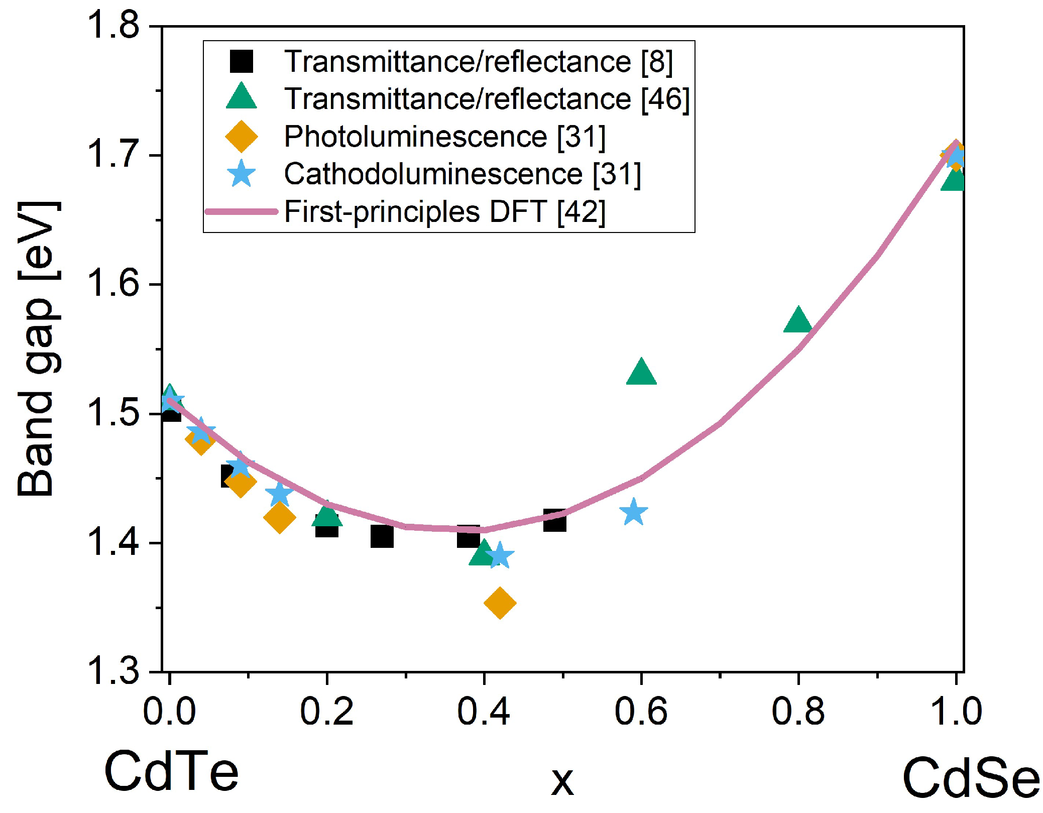
2.2. Optical Properties

CdTe1−xSex has a direct band gap with a pronounced bowing behavior. Figure 1 shows reported band gaps of CdTe1−xSex thin films measured with different methods, as well as one band gap bowing derived from first-principles DFT calculations, all showing a similar bowing behavior trend. The bowing parameter b can be extracted from experimental data with a second-degree polynomial fit. The band gap of any composition x can then be calculated using Equation (1) [42]:
E G ( x ) = x E G C d S e + ( 1 x ) E G C d T e b x ( 1 x )
Band gap bowing parameters from bulk and thin-film CdTe1−xSex, fabricated by different methods and using different measurement techniques, are listed in Table 1. The published bowing parameter values cover a range of 0.56–0.97, and they all agree on the composition of the band gap minimum at 0.3 ≤ x ≤ 0.4, independent of fabrication method. The bowing only marginally depends on the crystal structure [39]. The band gap determination using photoluminescence and cathodoluminescence seem to yield bowing parameters slightly higher than transmittance/reflectance measurements, but they are still in good agreement [31].
Theoretical calculations using different methods are also shown in Table 1, and they seem to be in good agreement with experimental data [42,43,44]. The band gap minima in all experiments and calculations are around 1.4 eV, confirming that CdTe1−xSex is a good candidate for band-gap engineering in CdTe solar cells for the purpose of increasing JSC.
In CdTe1−xSex, the valence band edge is dominated by Se and Te p-orbitals, and the conduction band edge is dominated by Cd s- and p-states. Therefore, the anion substitution would be expected to primarily affect the valence band edge [43,45]. However, first-principles calculations show that the bowing of the band gap is caused by the bowing of both band edges due to strong intra-band coupling in both the valence and the conduction band [44].
The refractive index of CdTe1−xSex is almost constant over a large range of wavelengths, as well as with changes in composition and film thickness. Use of a CdTe1−xSex layer is therefore not expected to change the overall reflectance of a solar cell, and the introduction of a CdTe1−xSex gradient does not introduce a gradient in the refractive index [7,25,32].

2.3. Electronic Properties

The electronic properties of CdTe1−xSex have not been studied extensively. As-deposited CdTe1−xSex is an n-type semiconductor with carrier densities between 1013 cm−3 (CdTe) and 1018 cm−3 (CdSe) [40]. The Hall mobility increases by less than an order of magnitude between CdTe and CdSe. Both carrier density and mobility are dependent on deposition temperature, with higher values at higher deposition temperatures due to increased grain size and possibly a reduction in structural defects [26,40]. In solar cell processing, the CdTe1−xSex layer is subjected to a CdCl2 treatment, during which it recrystallizes. In CdTe, the recrystallization results in larger grains, reduced structural defects, and reduced recombination [18,47]. A similar effect is expected for CdTe1−xSex. In absorbers consisting of a CdTe1−xSex layer in front of CdTe, recrystallization during CdCl2 treatment has been shown to be responsible for a reduction in stacking faults, combined with interdiffusion of the CdTe1−xSex and CdTe layers [19,28].
In solar cells that use CdTe1−xSex as part of the absorber layer, dopants are generally added to the whole CdTe1−xSex/CdTe stack and permeate the CdTe1−xSex layer via diffusion. A commonly used extrinsic dopant is copper, which forms deep acceptors as Cu on a Cd site (CuCd) [48,49]. First-principles calculations indicate that the formation energy of this acceptor defect exhibits a bowing, with lower formation energies in the CdTe1−xSex solid solution than in either parent compound [44]. In the mixed alloy, the bonding Te orbitals are partially replaced with Se orbitals, which have a lower energy. The electronic effects of this change in bonding orbitals are one reason for the bowing behavior. Another reason is the smaller lattice constant with increasing x leading to reduced compressive strain when Cd is replaced by the much smaller Cu [44]. The reduced formation energy indicates better dopability of CdTe1−xSex with copper compared to CdTe. However, Hall effect measurements of CdTe1−xSex with 0 ≤ x ≤ 0.2, deposited by high-vacuum evaporation and subjected to a CdCl2 treatment, revealed that the achievable doping concentration is lower in Se-containing samples, with more than an order of magnitude difference between CdTe and x = 0.2 [8]. A possible explanation is that compensating donors, such as copper on interstitial sites (Cui), are formed as well, and that the formation energy of these defects is also dependent on x. If the electronic and/or structural effects of CdTe1−xSex alloying facilitate the formation of compensating donors more than the formation of acceptor defects, the result is a limit to the achievable hole density [8,49,50].
The photoluminescence decay of CdTe1−xSex measured by time-resolved photoluminescence (TRPL) is generally dominated by surface recombination, resulting in short apparent lifetimes [23,51]. In order to get a reliable measure for the bulk minority carrier lifetime, the surface has to be passivated, e.g., using Al2O3, which provides field-effect passivation [52]. Another approach is two-photon excitation (2PE) TRPL, which allows for lifetime measurements at a selected depth of the absorber [51,53]. In CdTe1−xSex layers (x = 0.2, deposited by close space sublimation and subjected to CdCl2 treatment) with both surfaces passivated by sputtered Al2O3, lifetimes of up to 430 ns were measured, an order of magnitude higher than lifetimes in similarly passivated CdTe [23]. The reason seems to be that Se passivates a deep defect in the bulk of the absorber, even at low concentrations [19]. This is also correlated with longer diffusion length in material with higher x [13,19]. Two-photon excitation TRPL measurements performed on an interdiffused CdTe1−xSex/CdTe absorber (close space sublimation, CdCl2 treated, resulting maximum Se content x ≈ 0.16) have shown lifetimes of around an order of magnitude higher in the Se-rich front layer compared to the CdTe back layer. This lifetime difference within a single absorber was linked to reduced recombination at the grain boundaries in the Se-containing region [51,53]. Se therefore, at least up to x ≈ 0.2, seems to provide both passivation of a bulk defect and of the grain boundaries, resulting in an overall increased lifetime. Further studies are needed to accurately determine the lifetime dependence with x, and to determine the steepness of the lifetime gradient in an interdiffused CdTe1−xSex/CdTe absorber.
The various deposition methods used for CdSe or CdTe1−xSex apply a variety of substrate temperatures and deposition rates. We expect that the reported properties of CdTe1−xSex may depend on deposition method as well as on the parameters of the CdCl2 treatment, but further investigations are needed to determine the extent.

3. CdTe1−xSex in Solar Cells

In recent years, CdTe1−xSex has been used as a layer at the front of a predominantly CdTe absorber layer (see Figure 2), either deposited as CdSe or as CdTe1−xSex, which interdiffuse with CdTe during CdCl2 treatment to form a continuous composition gradient. This results in an absorber layer with a low band gap, increasing the JSC, and it allows for a reduction in CdS thickness, both in superstrate and substrate configuration. As a further step, Munshi et al. [15] replaced the CdS with MgZnO for the highest device efficiencies. Schematics of the different device configurations in which CdTe1−xSex layers have been used are shown in Figure 2, from CdS/CdTe1−xSex/CdTe (Figure 2b), to CdTe1−xSex/CdTe (Figure 2c), to MgZnO/CdTe1−xSex/CdTe (Figure 2d). As an alternative to the conventional superstrate configuration, a device in substrate configuration (Figure 2e) is discussed as well.
The best reported devices for each of the different structures in Figure 2 are listed in Table 2, as well as the CdTe1−xSex-containing record device by First Solar. By removing the CdS layer, a small increase in JSC and FF has been shown, due to reduced parasitic absorption of CdS, at the cost of some losses in VOC, due to interface recombination at the TCO/CdTe1−xSex interface [20]. With a MgZnO window layer, all device parameters could be improved: high JSC due to the absence of parasitic absorption in the window layer, and high VOC and FF due to a good band alignment between MgZnO and CdTe1−xSex, resulting in a power conversion efficiency of 19.1% [15]. For the substrate configuration device, while the FF is comparable to superstrate devices, the VOC and JSC are lower. The loss in VOC may be due to interface recombination at the CdS/CdTe1−xSex interface; the loss in JSC due to parasitic absorption in the remaining CdS layer [8]. The world record device from First Solar surpasses all other devices in terms of VOC and JSC, and only the MgZnO/CdTe1−xSex device can exceed its FF. The exact structure and therefore the reasons for this outstanding performance are not public knowledge, but the high JSC and VOC indicate the use of MgZnO or a similar window layer [3,9,10].
In the following section, we will first discuss the deposition methods used to form a CdTe1−xSex/CdTe solar cell absorber, and in subsequent subsections we will discuss the details of how CdTe1−xSex has been used to improve performance in devices with different configurations.

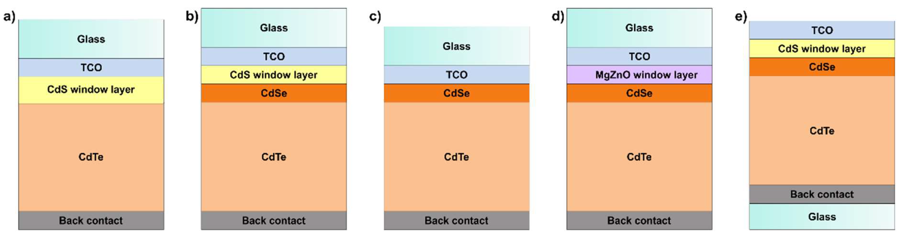
3.1. Formation of a CdTe1−xSex Layer during Device Processing

Different deposition methods have been used to form a CdTe1−xSex layer. In conventional superstrate configuration, CdSe can be deposited by high-vacuum evaporation [27], magnetron sputtering [14,16,47], or pulsed laser deposition [54], with CdTe1−xSex formation during CdCl2 treatment. An alternative is close-space sublimation (CSS) of a CdTe1−xSex layer [15,19,29]. The CdSe or CdTe1−xSex layer is followed by deposition of CdTe, CdCl2 and doping treatments, and back contact deposition.
For devices in substrate configuration, a CdSe layer is deposited onto CdTe, followed by CdCl2 and doping treatments and window layer/front contact deposition (see Figure 2e) [8].
In all of these device structures, the absorber and window layer are recrystallized and the CdSe/CdTe1−xSex interdiffuse with the CdTe during CdCl2 treatment. In an as-deposited CdTe1−xSex and CdTe absorber, a large number of small grains towards the front (CdTe1−xSex) and increasing grain size towards the back are observed, but after the CdCl2 treatment, the grains are uniform in size and no distinct boundary is visible between CdTe1−xSex and CdTe [28]. Scanning transmission electron microscopy (STEM)/energy-dispersive x-ray spectroscopy (EDS) mapping reveals interdiffusion of CdTe1−xSex and CdTe, with Se diffusing more than a µm into the CdTe layer [15,28]. Secondary ion mass spectrometry (SIMS) reveals accumulation of Se at grain boundaries in the CdTe layer, and a relative loss of Se at grain boundaries in the CdTe1−xSex layer, which is a strong indication for a combination of fast diffusion of Se along the grain boundaries and slow diffusion into the grains [19].
Any photons with energies above the CdTe band gap (≥1.5 eV) are absorbed in the CdTe1−xSex layer or in the CdTe absorber underneath. CdTe1−xSex has a lower band gap than CdTe (down to 1.4 eV), and it therefore absorbs photons that cannot be absorbed by CdTe. To maximize JSC gain, the CdTe1−xSex layer has to be sufficiently thick to absorb the majority of these photons with energies below the CdTe band gap. If it is formed from CdSe, the composition of the CdTe1−xSex layer after interdiffusion depends on the thickness of the deposited CdSe layer as well as on the annealing conditions. Yan et al. found that for CdSe layers up to 100 nm thick, the interdiffusion is sufficient to result in a completely photoactive zinc blende absorber with compositions of x ≤ 0.65. For thicker layers, a non-photoactive wurzite layer with x > 0.65 remains at the front of the absorber, which is undesirable because of parasitic absorption. With this method, it is difficult to achieve a thick photoactive layer for full absorption without formation of a non-photoactive layer [16,20,47]. Forming the CdTe1−xSex layer by depositing CdTe1−xSex with x ≤ 0.65 instead of CdSe allows for a higher overall Se content in the absorber because the risk of forming a non-photoactive wurzite layer is minimized, and thick photoactive low-band gap layers can be formed [15].
The interdiffusion of CdTe1−xSex and CdTe creates a compositional gradient, which is expected to be correlated to the gradient in the material properties of CdTe1−xSex, such as band gap, lattice constant, charge carrier concentration, and minority carrier lifetime. In particular, Fiducia et al. [19] reported gradients in both band gap and diffusion length (determined from cathodoluminescence measurements) that are directly correlated with the Se concentration gradient in a CdTe1−xSex/CdTe device.

3.2. Overview of Device Performances with CdTe1−xSex

Different research groups have had varying success in improving device performance using CdSe. Published device parameters are listed in Table 3, where the parameters are compared with reference devices without CdSe. Generally, the JSC could be improved by the reduced band gap and by reducing or removing the CdS layer. VOC losses are partially due to the reduced band gap. Further VOC losses together with fill factor losses have been mostly attributed to interface recombination, but they were not further investigated. The highest VOC was achieved by use of a MgZnO window layer instead of CdS. The deposition methods are also listed as they may have an influence on the material properties and device performance. The different approaches and results are discussed in the following subsections.

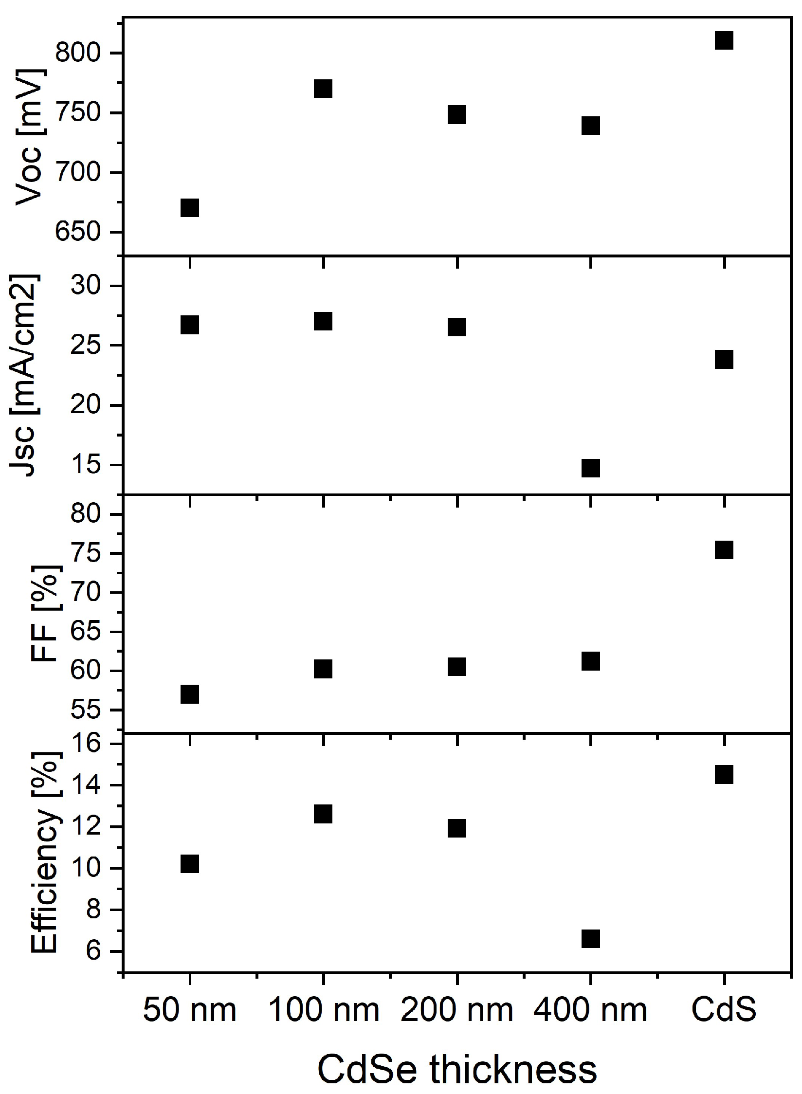
3.3. CdSe/CdTe Devices without a Window Layer

The performance of devices where the CdS window layer is completely substituted by a CdSe layer (Figure 2c) depends strongly on the thickness of the CdSe layer. Up to 100 nm thick CdSe layers completely interdiffuse with the CdTe during CdCl2 treatment, forming photoactive zinc blende CdTe1−xSex. This results in increased JSC compared to CdS/CdTe devices (see Figure 3) on the one hand because of increased absorption in the long-wavelength region due to a reduced band gap of the absorber, and on the other hand because the absorbing CdS layer is eliminated (see Figure 4). The overall efficiency however is still reduced because of losses in VOC and FF.
With thicker CdSe layers, the interdiffusion is not complete, and the JSC is reduced due to parasitic absorption in residual non-photoactive wurzite CdTe1−xSex with high Se content (x > 0.65). With optimized CdSe thickness, the JSC can be increased by more than 3 mA/cm2, however, this is not sufficient to offset the losses in VOC, which are attributed to high interface recombination at the direct contact between CdTe1−xSex and TCO [16,20].
The TCO used in CdTe and CdTe1−xSex/CdTe devices is usually a bilayer of a low-resistivity material, such as SnO2:F (FTO), and a high-resistivity material, such as SnO2. The highly resistive transparent (HRT) layer is used to prevent direct contact between the absorber and the FTO in the case of incomplete CdS coverage [55]. Baines et al. [12] investigated different oxides as HRT layers for CdTe1−xSex absorbers and found SnO2 to be the best. It reduces VOC losses that occur from direct contact of CdTe1−xSex with FTO, but the interface recombination is still higher than with a CdS layer [12,20]. In fact, the devices listed in Table 3 all use a SnO2 HRT layer.
With electron-beam induced current (EBIC) measurements the position of the junction can be determined: for up to 100 nm CdSe, the junction is located at the CdTe1−xSex/TCO interface. This reveals that the CdTe1−xSex does not act as a window layer, but as part of the p-side of the junction. For thicker CdSe layers, the junction is shifted into the CdTe1−xSex layer, to the interface between photoactive and non-photoactive CdTe1−xSex [16]. The VOC and JSC decrease for thicker layers, confirming that the presence of the non-photoactive wurzite CdTe1−xSex is not beneficial for the device performance. Deposition methods and parameters therefore have to be chosen to minimize the formation of non-photoactive CdTe1−xSex.

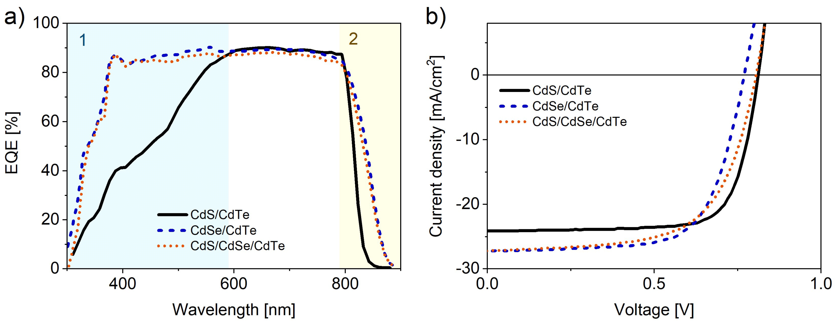
3.4. CdSe/CdTe Devices with a CdS Window Layer

With a combined CdS/CdSe window layer (Figure 2b), device performance can be increased by combining the upsides of both layers while minimizing the drawbacks (see Table 3). By reducing the CdS thickness from 130 nm in a CdS/CdTe device to 15 nm in a CdS/CdSe/CdTe device, the parasitic absorption in the short-wavelength region is minimized (region 1 in Figure 4a) and the JSC is increased. Further JSC increase is due to a shift in band gap with CdTe1−xSex (region 2 in Figure 4a). The JSC is therefore very similar to a CdSe/CdTe device, while the VOC is improved with the CdS layer in between the CdTe1−xSex and the TCO, which reduces the interface recombination (see Figure 4b) [20,54].
A CdS/CdSe/CdTe structure also works in substrate configuration solar cells (Figure 2e). Substrate configuration CdTe solar cells require a thick CdS layer in order to mitigate the formation of pinholes. With a CdTe1−xSex layer between CdTe and CdS, the CdS layer thickness can be reduced from 120 to 30 nm with only small losses in VOC and with a 7.1 mA/cm2 increase in JSC due to the reduction in CdS thickness and the reduction in band gap, resulting in an overall improvement in efficiency (see Table 3) [8].

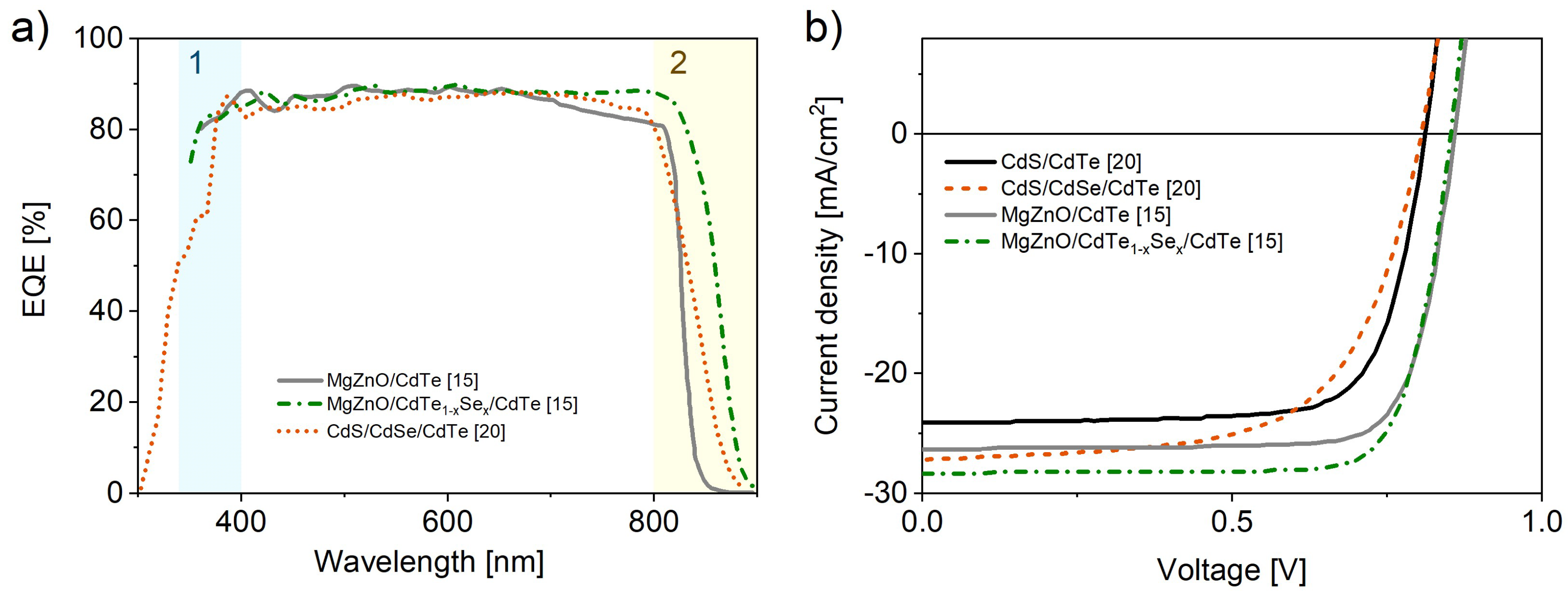
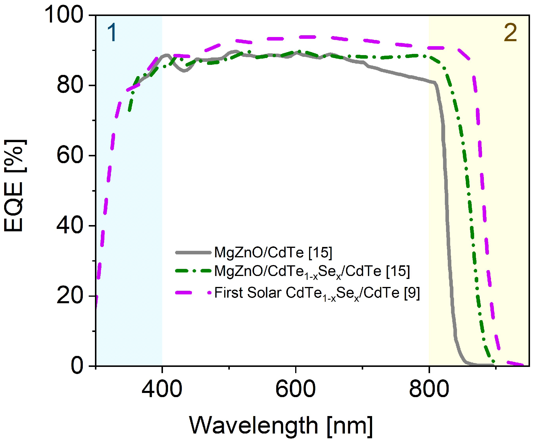
3.5. CdTe1-xSex/CdTe Devices with a MgZnO Window Layer

Recent high-efficiency CdTe devices have been achieved by replacing the CdS window layer with MgZnO (see Table 3) [15,22]. MgZnO has a band gap of 3.7 eV, higher than CdS, thereby reducing parasitic absorption, and it has a better band alignment with CdTe than TCO/CdS, reducing interface recombination and allowing for a higher VOC [21,22]. However, introduction of a MgZnO window layer into a device structure can be problematic. The MgZnO/CdTe interface is sensitive to barriers originating from oxides, e.g., MgO, that can be formed during deposition. To obtain high-efficiency MgZnO/CdTe devices, deposition parameters, such as temperature and oxygen partial pressure during deposition, and CdCl2 treatment, have to be carefully optimized [56].
Further improvement was achieved by using a CdTe1−xSex layer at the front of the CdTe absorber. With an 800 nm thick CdTe1−xSex layer in front of a CdTe absorber, Munshi et al. showed an improvement in device efficiency from 17.9% for a MgZnO/CdTe device to 19.1% in a MgZnO/CdTe1−xSex/CdTe device (see Table 3) [15]. They improved the JSC by 2.1 mA/cm2 while retaining the high VOC (see Figure 5a). As the device contains no CdS, the EQE in the short-wavelength region is improved (region 1 in Figure 5a).
The benefit of depositing CdTe1−xSex instead of CdSe in front of CdTe is the low possibility that non-photoactive wurzite CdTe1−xSex is formed. As a consequence, higher amounts of Se can be introduced to the device for better fine-tuning of the band gap gradient [29]. This results in a thicker photoactive low-band gap CdTe1−xSex layer in the finished device. The low-band gap region appears sufficiently thick to absorb most photons with energies below the band gap of CdTe, down to about 1.42 eV, as evidenced by the shift in absorption edge in the EQE curve in region 2 in Figure 5a. The difference in absorption between the thick photoactive layer achieved with CdTe1−xSex deposition and the thin photoactive layer achieved with CdSe deposition can be seen in the steepness of the EQE curve in region 2 in Figure 5a. The conclusion can be drawn that for maximized JSC gain from CdTe1−xSex, deposition of a CdTe1−xSex layer instead of a CdSe layer is necessary.
The high VOC in the MgZnO/CdTe1−xSex/CdTe device was in part attributed to a high lifetime of 22 ns measured by TRPL, four times higher than in the MgZnO/CdTe device, due to improved interface quality between MgZnO and CdTe1−xSex, and also due to the passivation of a recombination center by Se [13,15,19]. The MgZnO/CdTe1−xSex/CdTe device has a much higher VOC than the CdS/CdTe1−xSex/CdTe devices. This indicates that the VOC in these structures is limited by the TCO/CdS/CdTe1−xSex interfaces, but further investigations into the VOC and FF loss of CdTe1−xSex/CdTe devices is needed to confirm this.
Figure 6 compares the EQE curve of the high-efficiency MgZnO/CdTe1−xSex/CdTe device with the record device from First Solar. The First Solar device uses a CdTe1−xSex layer and some kind of buffer layer instead of CdS [11]. It has a higher VOC and higher JSC than the MgZnO/CdTe1−xSex/CdTe device (see Table 3) [3,11]. The increase in JSC is primarily due to a very good absorption at high wavelengths (region 2 in Figure 6). The very straight absorption edge indicates the presence of a sufficiently thick CdTe1−xSex layer with a band gap of 1.4 eV for complete absorption of photons in this region. Some further improvement of JSC is achieved by an overall higher EQE, probably due to an antireflection coating. In the short-wavelength region (region 1 in Figure 6), the curves are very similar. This is an indication that First Solar must have used MgZnO or a similar material as a buffer layer, eliminating the influence of parasitic absorption. The increase in VOC might be due to better interface engineering and therefore reduced recombination, but without more information on the First Solar device structure no conclusions can be drawn.

4. Conclusions

CdTe1−xSex has been successfully introduced into CdTe devices by several different groups. It has been shown that a band gap gradient can be achieved by several different techniques and deposition methods. For better control and a higher limit to the amount of Se put into the devices, use of a CdTe1−xSex layer is preferable to a CdSe layer in order to avoid formation of non-photoactive wurzite CdTeSe. In devices with a CdTe1−xSex layer at the front of the CdTe absorber, the reduced band gap and possibility of reduced CdS window layer thickness result in increased short-circuit current. The open circuit voltage can be maintained at the level of CdTe devices due to Se passivating a recombination center in the absorber. The best reported devices use a MgZnO window layer instead of CdS, which provides a better band alignment with the absorber and eliminates parasitic absorption from the window layer.

Funding

This research was funded by the Swiss National Science Foundation under the project 200021_160025/1.

Conflicts of Interest

The authors declare no conflict of interest.

References

  1. Philipps, S.; Warmuth, W. Photovoltaics Report; Fraunhofer ISE: Freiburg, Germany, 2019. [Google Scholar]
  2. First Solar Press Release. First Solar Achieves Yet another Cell Conversion Efficiency World Record; First Solar Press Release: Tempe, AZ, USA, 2016. [Google Scholar]
  3. Green, M.A.; Emery, K.; Hishikawa, Y.; Warta, W.; Dunlop, E.D. Solar cell efficiency tables (version 48). Prog. Photovolt. Res. Appl. 2016, 24, 905–913. [Google Scholar] [CrossRef] [Green Version]
  4. Geisthardt, R.M.; Topič, M.; Sites, J.R. Status and potential of CdTe solar-cell efficiency. IEEE J. Photovolt. 2015, 5, 1217–1221. [Google Scholar] [CrossRef]
  5. Shockley, W.; Queisser, H.J. Detailed balance limit of efficiency of p-n junction solar cells. J. Appl. Phys. 1961, 32, 510. [Google Scholar] [CrossRef]
  6. Rühle, S. Tabulated values of the Shockley–Queisser limit for single junction solar cells. Sol. Energy 2016, 130, 139–147. [Google Scholar] [CrossRef]
  7. Islam, R.; Banerjee, H.; Rao, D. Structural and optical properties of CdSexTe1−x thin films grown by electron beam evaporation. Thin Solid Films 1995, 266, 215–218. [Google Scholar] [CrossRef]
  8. Lingg, M.; Spescha, A.; Haass, S.G.; Carron, R.; Buecheler, S.; Tiwari, A.N. Structural and electronic properties of CdTe1−xSex films and their application in solar cells. Sci. Technol. Adv. Mater. 2018, 19, 683–692. [Google Scholar] [CrossRef]
  9. Green, M.A.; Emery, K.; Hishikawa, Y.; Warta, W.; Dunlop, E.D. Solar cell efficiency tables (version 46). Prog. Photovolt. Res. Appl. 2015, 23, 805–812. [Google Scholar] [CrossRef]
  10. Green, M.A.; Emery, K.; Hishikawa, Y.; Warta, W.; Dunlop, E.D. Solar cell efficiency tables (Version 45). Prog. Photovolt. 2015, 23, 1–9. [Google Scholar] [CrossRef]
  11. Gang, X.; Gloeckler, M. High Efficiency CdTe Solar Cells and Modules. In Proceedings of the E-MRS Spring Meeting, Strasbourg, France, 18–22 June 2018. [Google Scholar]
  12. Baines, T.; Zoppi, G.; Bowen, L.; Shalvey, T.P.; Mariotti, S.; DuRose, K.; Major, J.D. Incorporation of CdSe layers into CdTe thin film solar cells. Sol. Energy Mater. Sol. Cells 2018, 180, 196–204. [Google Scholar] [CrossRef]
  13. Fiducia, T.A.M.; Munshi, A.H.; Barth, K.; Proprentner, D.; West, G.; Sampath, W.S.; Walls, J.M. Defect tolerance in As-deposited selenium-alloyed cadmium telluride solar cells. In Proceedings of the 2018 IEEE 7th World Conference on Photovoltaic Energy Conversion (WCPEC) (A Joint Conference of 45th IEEE PVSC, 28th PVSEC & 34th EU PVSEC), Waikoloa Village, HI, USA, 10–15 June 2018; pp. 0127–0130. [Google Scholar]
  14. Mia, M.D.; Swartz, C.H.; Paul, S.; Sohal, S.; Grice, C.R.; Yan, Y.; Holtz, M.; Li, J.V. Electrical and optical characterization of CdTe solar cells with CdS and CdSe buffers—A comparative study. J. Vac. Sci. Technol. B 2018, 36, 052904. [Google Scholar] [CrossRef]
  15. Munshi, A.H.; Kephart, J.; Abbas, A.; Raguse, J.; Beaudry, J.-N.; Barth, K.; Sites, J.; Walls, J.; Sampath, W. Polycrystalline CdSeTe/CdTe absorber cells with 28 mA/cm2 short-circuit current. IEEE J. Photovolt. 2018, 8, 310–314. [Google Scholar] [CrossRef]
  16. Poplawsky, J.D.; Guo, W.; Paudel, N.; Ng, A.; More, K.; Leonard, D.; Yan, Y. Structural and compositional dependence of the CdTexSe1−x alloy layer photoactivity in CdTe-based solar cells. Nat. Commun. 2016, 7, 12537. [Google Scholar]
  17. Yang, X.; Liu, B.; Li, B.; Zhang, J.; Li, W.; Wu, L.; Feng, L. Preparation and characterization of pulsed laser deposited a novel CdS/CdSe composite window layer for CdTe thin film solar cell. Appl. Surf. Sci. 2016, 367, 480–484. [Google Scholar] [CrossRef]
  18. McCandless, B.E.; Moulton, L.V.; Birkmire, R.W. Recrystallization and sulfur diffusion in CdCl2-treated CdTe/CdS thin films. Prog. Photovolt. Res. Appl. 1997, 5, 249–260. [Google Scholar] [CrossRef]
  19. Fiducia, T.A.M.; Mendis, B.G.; Li, K.; Grovenor, C.R.M.; Munshi, A.H.; Barth, K.; Sampath, W.S.; Wright, L.D.; Abbas, A.; Bowers, J.W.; et al. Understanding the role of selenium in defect passivation for highly efficient selenium-alloyed cadmium telluride solar cells. Nat. Energy 2019, 4, 504–511. [Google Scholar] [CrossRef] [Green Version]
  20. Paudel, N.R.; Yan, Y. Enhancing the photo-currents of CdTe thin-film solar cells in both short and long wavelength regions. Appl. Phys. Lett. 2014, 105, 183510. [Google Scholar] [CrossRef]
  21. Kephart, J.; McCamy, J.; Ma, Z.; Ganjoo, A.; Alamgir, F.; Sampath, W. Band alignment of front contact layers for high-efficiency CdTe solar cells. Sol. Energy Mater. Sol. Cells 2016, 157, 266–275. [Google Scholar] [CrossRef] [Green Version]
  22. Munshi, A.H.; Kephart, J.M.; Abbas, A.; Shimpi, T.M.; Barth, K.L.; Walls, J.M.; Sampath, W.S. Polycrystalline CdTe photovoltaics with efficiency over 18% through improved absorber passivation and current collection. Sol. Energy Mater. Sol. Cells 2018, 176, 9–18. [Google Scholar] [CrossRef] [Green Version]
  23. Kephart, J.M.; Kindvall, A.; Williams, D.; Kuciauskas, D.; Dippo, P.; Munshi, A.; Sampath, W.S. Sputter-deposited oxides for interface passivation of CdTe photovoltaics. IEEE J. Photovolt. 2018, 8, 587–593. [Google Scholar] [CrossRef]
  24. Russak, M.A.; Creter, C. Vacuum Evaporated CdSe1−xTex Thin Films for Electrochemical Photovoltaic Cells. J. Electrochem. Soc. 1984, 131, 556–562. [Google Scholar] [CrossRef]
  25. El-Nahass, M.; Sallam, M.; Afifi, M.; Zedan, I. Structural and optical properties of polycrystalline CdSexTe1−x (0 ≤ x ≤ 0.4) thin films. Mater. Res. Bull. 2007, 42, 371–384. [Google Scholar] [CrossRef]
  26. Uthanna, S.; Reddy, P. Structural and electrical properties of CdSexTe1−x thin films. Solid State Commun. 1983, 45, 979–980. [Google Scholar] [CrossRef]
  27. Borah, M.N.; Chaliha, S.; Sarmah, P.; Rahman, A. Electrical and optical properties of thin film (n) CdSe/(p) CdTe heterojunction and its performance as a photovoltaic converter. J. Optoelectron. Adv. M. 2008, 10, 1333–1339. [Google Scholar]
  28. Munshi, A.H.; Kephart, J.M.; Abbas, A.; Danielson, A.; Gḗlinas, G.; Beaudry, J.-N.; Barth, K.L.; Walls, J.M.; Sampath, W.S. Effect of CdCl2 passivation treatment on microstructure and performance of CdSeTe/CdTe thin-film photovoltaic devices. Sol. Energy Mater. Sol. Cells 2018, 186, 259–265. [Google Scholar] [CrossRef]
  29. Swanson, D.E.; Sites, J.R.; Sampath, W.S. Co-sublimation of CdSexTe1x layers for CdTe solar cells. Sol. Energy Mater. Sol. Cells 2017, 159, 389–394. [Google Scholar] [CrossRef]
  30. Amir, F.; Clark, K.; Maldonado, E.; Kirk, W.; Jiang, J.; Ager III, J.; Yu, K.; Walukiewicz, W. Epitaxial growth of CdSexTe1−x thin films on Si (1 0 0) by molecular beam epitaxy using lattice mismatch graded structures. J. Cryst. Growth 2008, 310, 1081–1087. [Google Scholar] [CrossRef]
  31. Campo, E.M.; Hierl, T.; Hwang, J.C.; Chen, Y.; Brill, G.; Dhar, N.K. Comparison of cathodoluminescence and photoluminescence of CdSeTe films grown on Si by molecular beam epitaxy. In Proceedings of the SPIE, Denver, CO, USA, 22 October 2004. [Google Scholar]
  32. Muthukumarasamy, N.; Balasundaraprabhu, R.; Jayakumar, S.; Kannan, M.D.; Ramanathaswamy, P. Compositional dependence of optical properties of hot wall deposited CdSexTe1−x thin films. Phys. Status Solidi (a) 2004, 201, 2312–2318. [Google Scholar] [CrossRef]
  33. Mangalhara, J.; Agnihotri, O.; Thangaraj, R. Structural, optical and photoluminescence properties of electron beam evaporated CdSe1−xTex films. Sol. Energy Mater. 1989, 19, 157–165. [Google Scholar] [CrossRef]
  34. Bouroushian, M.; Loizos, Z.; Spyrellis, N.; Maurin, G. Influence of heat treatment on structure and properties of electrodeposited CdSe of Cd(Te, Se) semiconducting coatings. Thin Solid Films 1993, 229, 101–106. [Google Scholar] [CrossRef]
  35. Kathalingam, A.; Kim, M.R.; Chae, Y.S.; Rhee, J.K.; Thanikaikarasan, S.; Mahalingam, T. Study on electrodeposited CdSexTe1−x semiconducting thin films. J. Alloy. Compd. 2010, 505, 758–761. [Google Scholar] [CrossRef]
  36. McCandless, B.E.; Sites, J.R. Handbook of Photovoltaic Science and Engineering; John Wiley & Sons: Hoboken, NJ, USA, 2005; pp. 617–662. [Google Scholar]
  37. Strauss, A.J.; Steininger, J. Phase diagram of the CdTe-CdSe pseudobinary system. J. Electrochem. Soc. 1970, 117, 1420–1426. [Google Scholar] [CrossRef]
  38. Kumar, L.; Singh, B.P.; Misra, A.; Misra, S.; Sharma, T. Characterization of CdSexTe1−x sintered films for photovoltaic applications. Phys. B Condens. Matter 2005, 363, 102–109. [Google Scholar] [CrossRef]
  39. Tai, H.; Nakashima, S.; Hori, S. Optical properties of (CdTe)1−x(CdSe)x and (CdTe)1−x(CdS)x systems. Phys. Status Solidi (a) 1975, 30, K115–K119. [Google Scholar] [CrossRef]
  40. Russak, M.A. Deposition and characterization of CdSe1xTex thin films. J. Vac. Sci. Technol. A 1985, 3, 433–435. [Google Scholar] [CrossRef]
  41. Sanitarov, V.; Aleksandrova, L.; Kalinkin, I. The ranges of isomorphous substitutions in thin films of CdSexTe1x solid solutions. Thin Solid Films 1982, 97, 205–214. [Google Scholar] [CrossRef]
  42. Wei, S.H.; Zhang, S.; Zunger, A. First-principles calculation of band offsets, optical bowings, and defects in CdS, CdSe, CdTe, and their alloys. J. Appl. Phys. 2000, 87, 1304–1311. [Google Scholar] [CrossRef] [Green Version]
  43. Tit, N.; Obaidat, I.M.; Alawadhi, H. Origins of bandgap bowing in compound-semiconductor common-cation ternary alloys. J. Phys. Condens. Matter 2009, 21, 075802. [Google Scholar] [CrossRef]
  44. Yang, J.; Wei, S.-H. First-principles study of the band gap tuning and doping control in CdSexTe1−x alloy for high efficiency solar cell. Chinese Phys. B 2019, 28, 086106. [Google Scholar] [CrossRef]
  45. Reshak, A.H.; Kityk, I.; Khenata, R.; Auluck, S. Effect of increasing tellurium content on the electronic and optical properties of cadmium selenide telluride alloys CdSe1−xTex: An ab initio study. J. Alloy. Compd. 2011, 509, 6737–6750. [Google Scholar] [CrossRef]
  46. Santhosh, T.; Bangera, K.V.; Shivakumar, G. Synthesis and band gap tuning in CdSe1−xTex thin films for solar cell applications. Sol. Energy 2017, 153, 343–347. [Google Scholar] [CrossRef]
  47. Paudel, N.R.; Moore, K.L.; Yan, Y.; Poplawsky, J.D. Current enhancement of CdTe-based solar cells. IEEE J. Photovolt. 2015, 5, 1492–1496. [Google Scholar] [CrossRef]
  48. Krasikov, D.; Knizhnik, A.; Potapkin, B.; Selezneva, S.; Sommerer, T. First-principles-based analysis of the influence of Cu on CdTe electronic properties. Thin Solid Films 2013, 535, 322–325. [Google Scholar] [CrossRef]
  49. Wei, S.H.; Zhang, S.; Zhang, S.B. Chemical trends of defect formation and doping limit in II-VI semiconductors: The case of CdTe. Phys. Rev. B 2002, 66, 155211. [Google Scholar] [CrossRef]
  50. Gretener, C.; Wyss, M.; Perrenoud, J.; Kranz, L.; Buecheler, S.; Tiwari, A.N. CdTe thin films doped by Cu and Ag-a comparison in substrate configuration solar cells. In Proceedings of the 2014 IEEE 40th Photovoltaic Specialist Conference (PVSC), Denver, CO, USA, 8–13 June 2014; pp. 3510–3514. [Google Scholar]
  51. Kuciauskas, D.; Kanevce, A.; Burst, J.M.; Duenow, J.N.; Dhere, R.; Albin, D.S.; Levi, D.H.; Ahrenkiel, R.K. Minority carrier lifetime analysis in the bulk of thin-film absorbers using subbandgap (two-photon) excitation. IEEE J. Photovolt. 2013, 3, 1319–1324. [Google Scholar] [CrossRef]
  52. Kuciauskas, D.; Kephart, J.M.; Moseley, J.; Metzger, W.K.; Sampath, W.S.; Dippo, P. Recombination velocity less than 100 cm/s at polycrystalline Al2O3/CdSeTe interfaces. Appl. Phys. Lett. 2018, 112, 263901. [Google Scholar] [CrossRef]
  53. Zheng, X.; Kuciauskas, D.; Moseley, J.; Colegrove, E.; Albin, D.S.; Moutinho, H.; Duenow, J.N.; Ablekim, T.; Harvey, S.P.; Ferguson, A.; et al. Recombination and bandgap engineering in CdSeTe/CdTe solar cells. APL Mater. 2019, 7, 071112. [Google Scholar] [CrossRef]
  54. Yang, X.; Bao, Z.; Luo, R.; Liu, B.; Tang, P.; Li, B.; Zhang, J.; Li, W.; Wu, L.; Feng, L. Preparation and characterization of pulsed laser deposited CdS/CdSe bi-layer films for CdTe solar cell application. Mater. Sci. Semicond. Process. 2016, 48, 27–32. [Google Scholar] [CrossRef]
  55. Feldman, S.; Mansfield, L.; Ohno, T.; Kaydanov, V.; Beach, J.; Nagle, T. Non-uniformity mitigation in CdTe solar cells: The effects of high-resistance transparent conducting oxide buffer layers. In Proceedings of the Conference Record of the Thirty-first IEEE Photovoltaic Specialists Conference, Lake Buena Vista, FL, USA, 3–7 January 2005; pp. 271–274. [Google Scholar]
  56. Ablekim, T.; Perkins, C.; Zheng, X.; Reich, C.; Swanson, D.; Colegrove, E.; Duenow, J.N.; Albin, D.; Nanayakkara, S.; Reese, M.O.; et al. Tailoring MgZnO/CdSeTe Interfaces for Photovoltaics. IEEE J. Photovolt. 2019, 9, 888–892. [Google Scholar] [CrossRef]
Figure 1. Band gap bowing of CdTe1−xSex measured by different methods [8,31,46] and calculated from first-principles DFT [42].
Coatings 09 00520 g001
Figure 2. Schematics of deposited layers for solar cells (intermixing not depicted, thicknesses not to scale) for (a) a conventional CdTe device, (b) a device with a CdSe layer between CdTe and CdS [20]; (c) a device with CdSe replacing CdS [14,16]; (d) a device with MgZnO and CdSe replacing CdS [15]; and (e) a device in substrate configuration with a CdSe layer between CdTe and CdS [8].
Coatings 09 00520 g002
Figure 3. Performance of CdSe/CdTe solar cells with different CdSe thicknesses (values taken from Poplawsky et al. [16]).
Coatings 09 00520 g003
Figure 4. External quantum efficiency (EQE) (a) and J-V (b) curves of solar cells with different window layers (adapted from [20]).
Coatings 09 00520 g004
Figure 5. EQE (a) and J-V (b) curves of MgZnO/CdTe and MgZnO/CdTe1−xSex/CdTe devices (adapted from [15]) compared with a CdS/CdSe/CdTe device (adapted from [20]).
Coatings 09 00520 g005
Figure 6. EQE curves of Munshi et al. (adapted from [15]) and the First Solar record device (adapted from [9]).
Coatings 09 00520 g006
Table 1. Band gap bowing parameters of layers and powders synthesized with different methods.
SourceDepositionBand Gap DeterminationCrystal Structurex RangeBowing Parameterx of Band Gap MinimumBand Gap Minimum
[39]Sintering of mixed CdTe and CdSe powdersTransmittance/reflectancezinc blende0–0.60.740.351.38
[39]Sintering of mixed CdTe and CdSe powdersTransmittance/reflectancewurzite0.4–10.680.331.4
[8]Co-evaporation of CdTe and CdSeTransmittance/reflectancezinc blende0–0.50.780.371.39
[7]Electron-beam evaporationTransmittance/reflectancezinc blende0–10.5670.371.44
[46]Thermal evaporation of mixed CdTe and CdSe powdersTransmittance/reflectancezinc blende0–10.5710.351.44
[31]Molecular beam epitaxy on SiPhotoluminescencezinc blende0–10.970.401.35
[31]Molecular beam epitaxy on SiCathodoluminescencezinc blende0–10.820.381.39
[42]First-principles DFT calculationszinc blende0–10.750.401.41
[43]sp3s* tight-binding method calculationszinc blende0–10.9040.391.37
[44]First-principle hybrid-functional calculationszinc blende0–10.7250.391.43
Table 2. J-V parameters of the best CdTe1−xSex-containing devices for each configuration shown in Figure 2.
SourceDevice StructureVOC
[mV]
JSC
[mA/cm2]
FF
[%]
Efficiency
[%]
Paudel and Yan [20]Figure 2b80627.264.114.1
Paudel and Yan [20]Figure 2c77127.569.414.7
Munshi et al. [15]Figure 2d85428.479.119.1
Lingg et al. [8]Figure 2e71025.66712.2
First Solar [3,9,10]unknown887.231.6978.522.1
Table 3. J-V parameters of devices containing CdSe compared with non-CdSe devices. Deposition methods are abbreviated as RFS (radio frequency sputtering), CSS (close space sublimation), and HVE (high vacuum evaporation).
SourceDevice StructureVOC
[mV]
JSC
[mA/cm2]
FF
[%]
Efficiency
[%]
Poplawsky et al. [16]CdSe (100 nm, RFS)/CdTe (CSS)7702760.212.6
CdS (130 nm, RFS)/CdTe (CSS)81023.875.414.5
difference with CdSe−40+3.2−15.2−1.9
Mia et al. [14]CdSe (100 nm, RFS)/CdTe (CSS)69026.964.812.1
CdS (140 nm, RFS)/CdTe (CSS)84724.77014.6
difference with CdSe−157+2.2−5.2−2.5
Paudel and Yan [20]CdSe (100 nm RFS)/CdTe (CSS)77127.569.414.7
CdS (15 nm, RFS)/CdSe (100 nm, RFS)/CdTe (CSS)80627.264.114.1
CdS (130 nm, RFS)/CdTe (CSS)81124.275.514.8
difference only CdSe−40+3.3−6.1−0.1
difference mixed CdS/CdSe−5+3−11.4−0.7
pLingg et al. [8]CdS (30 nm)/CdSe (60 nm)/CdTe (all HVE, substrate config.)71025.66712.2
CdS (120 nm)/CdTe (all HVE, substrate config.)83018.569.410.5
difference with CdSe−120+7.1−2.4+1.7
Munshi et al. [15]MgZnO (RFS)/CdTe0.8Se0.2 (800 nm, CSS)/CdTe (CSS)85428.479.119.1
MgZnO (RFS)/CdTe (CSS)86026.378.917.9
difference with CdSe−6+2.1+0.2+1.2
First Solar [3,9,10]CdTe1−xSex/CdTe *887.231.6978.522.1
CdS/CdTe *875.930.2579.421
difference with CdSe+11.3+1.44−0.9+1.1
* The exact device structures and methods of deposition used in the First Solar record devices are not public knowledge.

