Article

Double-Sided Anti-Reflection Nanostructures on Optical Convex Lenses for Imaging Applications

1
School of Electrical Engineering and Computer Science (EECS), Gwangju Institute of Science and Technology (GIST), 123 Chemdangwagi-ro, Buk-gu, Gwangju 61005, Korea
2
Division of Scientific Instrumentation, Korea Basic Science Institute, 169-148 Gwahak-ro, Yuseong-gu, Daejeon 306-806, Korea
*
Authors to whom correspondence should be addressed.
These authors contributed equally to this work.
Coatings 2019, 9(6), 404; https://doi.org/10.3390/coatings9060404
Submission received: 2 May 2019 / Revised: 18 June 2019 / Accepted: 19 June 2019 / Published: 21 June 2019
(This article belongs to the Special Issue Semiconductor Thin Films)

Abstract

:
Anti-reflection coatings (ARCs) from the cornea nipple array of the moth-eye remarkably suppress the Fresnel reflection at the interface in broadband wavelength ranges. ARCs on flat glass have been studied to enhance the optical transmittance. However, little research on the implementation of ARCs on curved optical lenses, which are the core element in imaging devices, has been reported. Here, we report double-sided, bio-inspired ARCs on bi-convex lenses with high uniformity. We theoretically optimize the nanostructure geometry, such as the height, period, and morphology, since an anti-reflection property results from the gradually changed effective refractive index by the geometry of nanostructures. In an experiment, the transmittance of an ARCs lens increases up to 10% for a broadband spectrum without distortion in spot size and focal length. Moreover, we demonstrate ~30% improved transmittance of an imaging system composed of three bi-convex lenses, in series with double-sided ARCs (DARCs).

Graphical Abstract

1. Introduction

Nanostructured surfaces in nature feature multi-functionalities, such as self-cleaning of the lotus leaf, vivid color of butterfly wings, photoreception of brittlestars, and broadband antireflection of the moth-eye cornea [1,2,3,4,5]. Owing to their intriguing features, these intelligent biological structures motivated the development of biomimetic engineering. In particular, the anti-reflection effect originated from a gradual change in the effective refractive index due to the tapered nanostructures in which the volume ratio changes continuously in a vertical direction [6]. Using these phenomena, reduced light reflection can be dramatically achieved at a broad range of wavelengths [6]. Anti-reflection coatings (ARCs) have been extensively studied in optoelectronics for efficient light management, such as in light-emitting diodes and solar cells exploiting the aforementioned functions. [7,8,9]. Numerous manufacturing processes have been developed with the increasing demand for ARCs. By introducing these processes, anti-reflection nanostructures can be produced on typical materials, such as glass, Si, GaN, and GaAs on a flat surface by manipulating the geometries for index matching to a refractive index of air (e.g., ion implantation, dry etching with a thermal dewetted metal mask, holo-lithography, and nanoimprint lithography [6,10,11]).
Recently, due to the emergence of versatile formation with optical materials, there has been growing interest in nanostructures on curved surfaces for optical applications. In particular, in multi-lens imaging system applications at broadband wavelengths (e.g., photo-thermal optical coherence tomography (OCT) and nonlinear optical (NLO) microscopy) [12,13,14], the optical losses of each single optical component are continuously accumulated, meaning that the performance of optical systems is significantly affected. Although research on nanostructures in relation to optical properties with curved surfaces, such as convex or concave optical lenses has been conducted, only a small body of results has been reported [15,16,17,18], and optical design with a theoretical background has not been sufficiently optimized for practical applications at a wide range of wavelengths. Among the results reported thus far, optical lenses using ARCs showed diffraction at a short wavelength of 300–400 nm, which resulted in a lower transmittance than conventional lenses at shorter wavelengths. In addition, the fabrication methods are often complex and expensive, and few ARCs on both sides of lenses covering wavelengths longer than 1000 nm without high-order diffraction have been reported.
In this work, we demonstrate double-side antireflection coatings (DARCs) on bi-convex BK7 and SF11 lenses with a simple fabrication method. DARCs lenses display the improved transmittances at a broadband wavelength from 300 to 1600. More specifically, the transmittances are maximally improved ~10% at the wavelengths of 425 and 540 nm for BK7 and SF11 lenses, respectively. They also exhibit no high-order diffraction and differences in focal length and spot size, compared to bare lenses. Furthermore, we design an optical system in which two BK7 lenses and one SF11 lens are configured in sequence. Our designed optical system exhibits an enhanced transmittance of about 30%, and offers potential for higher optical performance in multi-lens imaging devices.

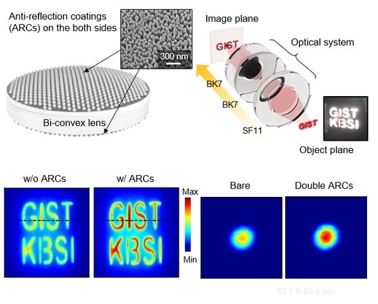
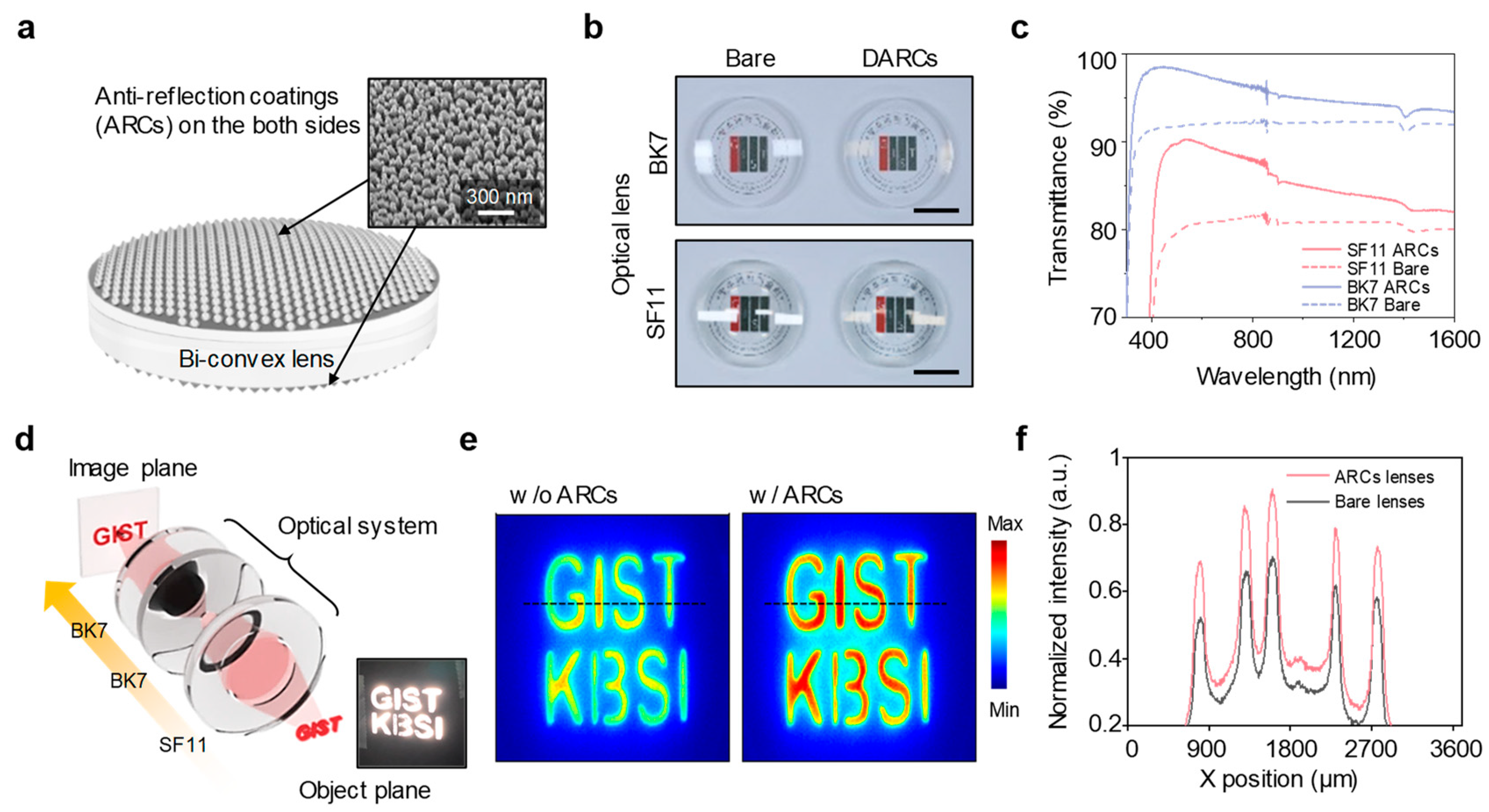
2. Optical Imaging of Bi-Convex Lenses with Double-Side Antireflection Coatings

Figure 1a shows a schematic illustration of a bi-convex lens with double-side antireflection coatings (DARCs). Truncated cone-shaped SiO2 nanostructures were applied to both sides of the optical lenses as our designed DARCs. A scanning electron microscope (SEM) image here shows a tilted top view of a fabricated BK7 lens. The period of the nanostructures was small enough, compared to a width of 300 nm. As shown in Figure 1b, we fabricated DARCs on both sides of two types of optical lenses (i.e., BK7 and SF11). The main information of the optical lenses, including material and optical properties, is provided in Table 1. DARCs lenses not only provide clear images, but also suppress the light reflection due to an anti-reflection effect, compared to bare lenses. Figure 1c exhibits the measured transmittance of the lenses, given in Figure 1b, as a function of the wavelength from 300 to 1600 nm. The solid and dashed lines represent the DARCs and bare lenses, respectively. The maximum enhanced transmittance is up to 10% on both the SF11 lens and BK7 lens.
The spatial uniformity of DARCs is also demonstrated by the measuring of optical powers using three monochromatic lights at different lens positions (Figure S1). The measured results show that DARCs lens demonstrate the overall transmittance regardless of wavelengths and positions (Figure S2). The degradation over 10 mm is explained by the multiple total internal reflection in the lens (Figures S3 and S4). For optical imaging with DARCs lenses, the optical system consists of two BK7 lenses and one SF11 lens, as presented in Figure 1d. As an optical object, a 3D printed mask with a surface light source was used (Figure 1d, bottom right). Figure 1e shows a comparison of the intensity profiles, which was obtained by a charge-coupled device (CCD) from an optical system with three bare lenses (left) and three DARCs lenses (right). Figure 1f exhibits the normalized intensity of the dashed line in Figure 1e. The results suggest that the transmittance was improved by up to 30%, compared to the optical system without DARCs. From these results, in practical applications, higher transmittance improvement is expected with the application of DARCs to multi-lens optical systems with more than 10 lenses [19].

3. Simulation and Optimization of Geometry of Nanostructures

The anti-reflection property is tunable with geometrical parameters, such as height, period, and morphology of nanostructures. The nanostructure geometry has to be considered to prevent light-scattering, causing an opaque surface [20]. We simulated the transmittance with SF11 glass and SiO2 nanostructures in terms of these parameters by using the rigorous coupled-wave analysis (RCWA) method. Moreover, electric field distributions, in terms of period, were calculated by using the RCWA method, which shows whether diffraction occurs. Also, periodic nanostructures were simulated because the non-periodic nanostructures have an anti-reflection effect that is comparable to that of periodic nanostructures [21]. Figure 2a shows a schematic illustration of three geometrical SiO2 nanostructure arrays with rods, truncated cones, and cones. The parameters of period (p), height (h), bottom width (w2), and top width (w1) are shown in Figure 2a. Also, we defined the filling fraction as a percentage of w2/p, and the cone ratio (CR) as the ratio of w1 to w2 (i.e., a CR of 100% means a cone-shaped nanostructure). The CR of 0, 50%, and 100% correspond to a rod, truncated cone, and cone shape, respectively.
The nanostructures morphology was optimized as a truncated cone shape (transmittance spectra of the three different nanostructure shapes are provided in Figures S5 and S6). Rod-shaped nanostructures show a nontrivial decrease of transmittance in a short wavelength of 400–600 nm. The cone-shaped geometry displays lower transmittance at the overall wavelength than the truncated-cone geometry. On the other hand, in the case of the truncated-cone nanostructure, transmittance is moderately improved at broadband wavelengths from 400 to 1600 nm.
Figure 2b exhibits the transmittance profile as a function of wavelength from 400 to 1600 nm in terms of period, height, and filling fraction. We calculated the transmittance in terms of the period at the conditions of a filling fraction of 100%, height of 150 nm, and cone ratio of 50%. The transmittance was enhanced until a period of 300 nm. However, the transmittance gradually degrades at above 300 nm due to the generation of multiple diffraction orders [22,23]. Therefore, we adopted the period of 200 nm. Since, in the fabrication method, we introduced randomly distributed Silver (Ag) nanoparticles for a hard mask, which shows the trade-off between the height and period [23], height was optimized to 150 nm for the diffraction-free period. A higher filling fraction showed better transmittance at overall wavelengths due to the moderate change in the effective refractive index and a smaller difference in the refractive index at interfaces [24,25].
Figure 2c displays the average transmittance at a wavelength range of 400–1600 nm as a function of CR, which displays better transmission efficiency than bare glass in all morphologies. As depicted in Figure 2d, average transmittance, at wavelengths from 400 to 1600 nm, is calculated as a function of the incident angle, which shows improved transmittance compared to bare glass. In particular, the anti-reflection performance is relatively uniform within 50°.
It is also necessary to consider the diffraction, which degrades the imaging performance, as well as transmittance [26]. Figure 2e depicts the diffraction efficiency according to a period at 200 (left) and 500 nm (right). As we mentioned in relation to Figure 1b, only a 0th order diffraction occurs at a period of 200 nm, whereas at 500 nm, multiple diffraction orders are produced. Figure 2f shows the electric field profiles in Figure 2e. The propagated plane wave is diffracted through the nanostructures with a period of 500 nm. On the other hand, at a period of 200 nm, the plane wave is not distorted, which indicates that multiple diffraction did not occur.

4. Fabrication of Nanostructures on Both Sides of the Bi-Convex Lens

Figure 3a depicts the schematic illustration of the ARCs fabrication process. We exploited a simple fabrication strategy which was lithography-free. Furthermore, our fabrication process was also available to most types of SiO2-based lenses by the same process, due to a refractive index of SiO2 with almost no difference compared to other SiO2-based lenses. A SiO2 layer of 150 nm was deposited for anti-reflection structures via RF sputtering. As optical lenses are composed of various materials as well as pure SiO2, the etching rate differs from each other. Therefore, we introduced a SiO2 layer to fabricate ARCs under the identical condition for simple and universal applications. In order to form Ag nanoparticles, a thin Ag film of 10 nm was deposited via an electron beam evaporator, and then the film was thermally dewetted for a hard mask by rapid thermal annealing (RTA) at 500 °C for 1 min with a N2 ambient of 200 mTorr. Reactive ion etching (RIE, Oxford Plasmalab 80 Plus, Abingdon, UK) was subsequently performed to fabricate a truncated cone of SiO2 where the CF4 flow, chamber pressure, temperature, and RF power were 50 sccm, 30 mTorr, 23 °C, and 100 W, respectively. After SiO2 etching, Ag residues were removed via nitric acid (HNO3) for 1 min at room temperature. Finally, the fabricated optical lenses were cleaned using acetone, isopropyl alcohol (IPA), and deionized (DI) water, and dried with N2 blowing. These steps were repeated for the other side of the optical lens. Figure 3b presents the SEM images of the top view in terms of position at the center, right-middle, and the right edge. As shown in Figure 3b, the nanostructures were fairly well-formed on the surface of both the BK7 and SF11 lenses. Figure 3c exhibits the filling fraction in terms of position in Figure 3b. Both DARCs lenses, BK7 and SF11, were implemented with nanostructures having a filling fraction between 60% and 80%. The size distribution and fast-fourier transform (FFT) profiles were plotted to figure out the nanostructure geometry on the lens depending on the position, in Figure S7.

5. Imaging Properties of Fabricated Single Lens

We also estimated the optical imaging properties of the DARCs lenses. For practical use of the designed optical system, the fabricated bi-convex lenses should maintain its original optical properties, such as the focal length and spot size, except for the transmittance. Figure 4a shows a schematic illustration of the optical setup for estimating imaging properties. Laser diodes having wavelengths of 520, 635, and 980 nm were used as a point light source. Optical components were introduced as a beam expander to evaluate the broad region of the lens, as well as an aperture to screen unnecessary light. In addition, the optical lens was moved back and forth with the micro-stage. Light intensity was obtained from an image sensor based on silicon (Basler acA3800-14um with pixel pitch of 1.67 μm). Figure 4b exhibits the measured beam profile (50 × 50 pixels) of the SF11 bare and DARCs lens, which shows the improved transmittance of the SF11 DARCs lens. Compared with the intensity of a SF11 bare lens, that of the SF11 DARCs lens displays the improved intensity. Also, the white dashed line depicts the baselines at which the Gaussian beam profile is presented. In the case of a curved surface, the film thickness can vary depending on the deposition position [27]. The different deposition site can impact minor differences in the nanostructure’s height. Therefore, the sputter method was used for film thickness uniformity. As shown in Figure 4b, there were no impacts on imaging quality, since the densely packed SiO2 cone array was formed with small periodicity and width.
Figure 4c presents a comparison between the peak intensity and power enhancement ratio of the SF11 bare lens and DARCs lens as a function of position. As shown in Figure 4c, the position of maximum peak intensity of SF11 DARCs lens is not changed, compared to the SF11 bare lens (vertical dashed line), which indicates the identical focal length [28]. In addition, the enhancement ratio was calculated by the DARCs peak intensity divided by the bare peak intensity, which displayed how the transmission at the center was more efficiently enhanced, up to 30%. Figure 4d shows a comparison of the full width at half maximum (FWHM) of the intensity profile in Figure 4b in terms of the x and y directions, which indicates a trivial difference of the FWHM [29]. In fact, the DARCs lens improved the transmittance compared to the bare lens without creating changes in focal length or spot size. Our proposed structure was meant to improve the transmittance without light diffraction and scattering. In our experiment, we introduced the two optical lenses which had different radii of curvatures (45.61 and 123.17 mm, Table 1). The randomly distributed nanostructures were uniformly formed on these curved surfaces with enhanced optical properties. Our method is applicable to other curved components, such as doublets and axicons, and has a simple and easy fabrication method.

6. Conclusions

In summary, we numerically optimized the geometrical parameters by using RCWA to meet an optimal anti-reflection property which came from a gradual change in the effective refractive index. We successfully implemented the truncated nanostructures with high uniformity on both sides of the bi-convex lenses comprised of a BK7 and SF11 lens. In addition, due to the introduction of a buffered layer of SiO2, our fabrication method is applicable to various lenses with an identical fabrication process. In regard to the optical performance, our DARCs lenses displayed up to 10% improved transmittance at broadband wavelengths from 400 to 1600 nm without distortion of spot size and focal length. Furthermore, we designed the optical system, composed of three DARCs lenses, and obtained the letter image which showed up to 30% enhanced transmission compared to three bare lenses. From this result, a higher anti-reflection effect can be expected in more complex optical systems, particularly those with a wide range of wavelengths from visible to near-infrared regions. Moreover, we believe that our proposed antireflection coating with an oxide buffer layer can be extended to wider applications with curved surfaces, such as eyewear, windows, and displays.

Supplementary Materials

The following are available online at https://www.mdpi.com/2079-6412/9/6/404/s1, Figure S1: Schematic of measurement setup for transmittance enhancement of DARCs lens with different positions, Figure S2: Measured transmittances of bare, one-sided, and double-sided ARCs lens, Figure S3: Ray-tracing results on bi-convex lens at different beam positions, Figure S4: Detected optical power in terms of simulation, Figure S5: Contour plots of calculated transmittance spectra as a function of period for glass materials, Figure S6: Contour plots of calculated transmittance spectra as a function of height for glass materials, Figure S7: Bar plot of the island size distribution depending on the positions and lens materials.

Author Contributions

Conceptualization, H.J.J., Y.J.K., Y.J.Y., G.J.L. and M.S.K.; Methodology, H.J.J. and Y.J.K.; Validation, H.J.J. and Y.J.Y.; Formal Analysis, H.J.J. and Y.J.Y.; Investigation, H.J.J. and G.J.L.; Resources, H.J.J.; Data Curation, H.J.J. and Y.J.K.; Writing—Original Draft Preparation, H.J.J.; Writing—Review and Editing, H.J.J., Y.J.K., G.J.L., M.S.K., Y.J.Y. and Y.M.S.; Supervision, Y.M.S. and K.S.C.

Funding

This work was supported by Agency for Defense Development of Korea and Defense Acquisition Program Administration Grant UD170079FD, the Korea Basic Science Institute (KBSI) Grant (D39615), and the National Research Foundation (NRF) of Korea (NRF-2018R1A4A1025623).

Conflicts of Interest

The authors declare no conflict of interest.

References

  1. Potyrailo, R.A.; Ghiradella, H.; Vertiatchikh, A.; Dovidenko, K.; Cournoyer, J.R.; Olson, E. Morpho butterfly wing scales demonstrate highly selective vapour response. Nat. Photonics 2007, 1, 123–128. [Google Scholar] [CrossRef]
  2. Nakata, K.; Sakai, M.; Ochiai, T.; Murakami, T.; Takagi, K.; Fujishima, A. Antireflection and self-cleaning properties of a moth-eye-like surface coated with TiO2 particles. Langmuir 2011, 27, 3275–3278. [Google Scholar] [CrossRef] [PubMed]
  3. Aizenberg, J.; Tkachenko, A.; Weiner, S.; Addadi, L.; Hendler, G. Calcitic microlenses as part of the photoreceptor system in brittlestars. Nature 2001, 412, 819–822. [Google Scholar] [CrossRef] [PubMed]
  4. Song, Y.M.; Xie, Y.; Malyarchuk, V.; Xiao, J.; Jung, I.; Choi, K.J.; Liu, Z.; Park, H.; Lu, C.; Kim, R.H.; et al. Digital cameras with designs inspired by the arthropod eye. Nature 2013, 497, 95–99. [Google Scholar] [CrossRef] [PubMed]
  5. Bernhard, C.G. Structural and functional adaptation in a visual system. Endeavour 1967, 26, 79–84. [Google Scholar]
  6. Huang, Y.F.; Chattopadhyay, S.; Jen, Y.J.; Peng, C.Y.; Liu, T.A.; Hsu, Y.K.; Pan, C.L.; Lo, H.C.; Hsu, C.H.; Chang, Y.H.; et al. Improved broadband and quasi-omnidirectional anti-reflection properties with biomimetic silicon nanostructures. Nat. Nanotechnol. 2007, 2, 770–774. [Google Scholar] [CrossRef] [PubMed]
  7. Kim, J.J.; Lee, Y.; Kim, H.G.; Choi, K.J.; Kweon, H.S.; Park, S.; Jeong, K.H. Biologically inspired LED lens from cuticular nanostructures of firefly lantern. PNAS 2012, 109, 18674–18678. [Google Scholar] [CrossRef] [PubMed] [Green Version]
  8. Tavakoli, M.M.; Tsui, K.H.; Zhang, Q.; He, J.; Yao, Y.; Li, D.; Fan, Z. Highly efficient flexible perovskite solar cells with antireflection and self-cleaning nanostructures. ACS Nano 2015, 9, 10287–10295. [Google Scholar] [CrossRef] [PubMed]
  9. Kim, Y.J.; Lee, G.J.; Kim, S.; Min, J.W.; Jeong, S.Y.; Yoo, Y.J.; Lee, S.; Song, Y.M. Efficient light absorption by GaN truncated nanocones for high performance water splitting applications. ACS Appl. Mater. Interfaces 2018, 10, 28672–28678. [Google Scholar] [CrossRef]
  10. Kadakia, L.; Naczas, S.; Bakhru, H.; Huang, M. Fabrication of surface textures by ion implantation for antireflection of silicon crystals. Appl. Phys. Lett. 2010, 97, 191912. [Google Scholar] [CrossRef]
  11. Song, Y.M.; Jang, S.J.; Yu, J.S.; Lee, Y.T. Bioinspired parabola subwavelength structures for improved broadband antireflection. Small 2010, 6, 984–987. [Google Scholar] [CrossRef] [PubMed]
  12. Tucher-Schwartz, J.M.; Breavers, K.R.; Sit, W.W.; Shah, A.T.; Duvall, C.L.; Skala, M.C. In vivo imaging of nanoparticle delivery and tumor microvasculature with multimodal optical coherence tomography. Biomed. Opt. Express 2014, 5, 1731–1743. [Google Scholar] [CrossRef] [PubMed] [Green Version]
  13. Latour, G.; Robinet, L.; Dazzi, A.; Portier, F.; Deniset-Besseau, A.; Schanne-Klein, M.C. Correlative nonlinear optical microscopy and infrared nanoscopy reveals collagen degradation in altered parchments. Sci. Rep. 2016, 6, 26344. [Google Scholar] [CrossRef] [PubMed] [Green Version]
  14. Vogler, N.; Heuke, S.; Bocklitz, T.W.; Schmitt, M.; Popp, J. Multimodal imaging spectroscopy of tissue. Annu. Rev. Anal. Chem. 2015, 8, 359–387. [Google Scholar] [CrossRef] [PubMed]
  15. Su, W.X.; Wu, C.Y.; Lee, Y.C. Anti-reflection nano-structures fabricated on curved surface of glass lens based on metal contact printing lithography. Microelectron. Eng. 2019, 214, 15–20. [Google Scholar] [CrossRef]
  16. Lee, Y.; Bae, S.I.; Eom, J.; Suh, H.C.; Jeong, K.H. Antireflective glass nanoholes on optical lenses. Opt. Express 2018, 26, 14786–14791. [Google Scholar] [CrossRef] [PubMed]
  17. Park, S.C.; Kim, N.; Ji, S.; Lim, H. Fabrication and characterization of moth-eye mimicking nanostructured convex lens. Microelectron. Eng. 2016, 158, 35–40. [Google Scholar] [CrossRef]
  18. Mano, I.; Uchida, T.; Taniguchi, J. Fabrication of the antireflection structure on aspheric lens surface and lens holder. Microelectron. Eng. 2018, 191, 97–103. [Google Scholar] [CrossRef]
  19. Xie, R.; Su, J.; Rentchler, E.C.; Zhang, Z.; Johnson, C.K.; Shi, H.; Hui, R. Multi-modal label-free imaging based on a femtosecond fiber laser. Biomed. Opt. Express 2014, 5, 2390–2396. [Google Scholar] [CrossRef] [Green Version]
  20. Perera, M.N.M.N.; Schmidt, D.; Gibbs, W.E.K.; Juodkazis, S.; Stoddart, P.R. Effective optical constants of anisotropic silver nanoparticle films with plasmonic properties. Opt. Lett. 2016, 41, 5495–5498. [Google Scholar] [CrossRef]
  21. Lin, C.; Huang, N.; Povinelli, M.L. Effect of aperiodicity on the broadband reflection of silicon nanorod structures for photovoltaics. Opt. Express 2012, 20, A125–A132. [Google Scholar] [CrossRef]
  22. Song, Y.M.; Choi, H.J.; Yu, J.S.; Lee, Y.T. Design of highly transparent glasses with broadband antireflective subwavelength structures. Opt. Express 2010, 18, 13063–13071. [Google Scholar] [CrossRef] [PubMed]
  23. Park, G.C.; Song, Y.M.; Ha, J.H.; Lee, Y.T. Broadband antireflective glasses with subwavelength structures using randomly distributed Ag nanoparticles. J. Nanosci. Nanotechnol. 2011, 11, 6152–6156. [Google Scholar] [CrossRef] [PubMed]
  24. Nam, W.I.; Yoo, Y.J.; Song, Y.M. Geometrical shape design of nanophotonic surfaces for thin film solar cells. Opt. Express 2016, 24, A1033–A1044. [Google Scholar] [CrossRef] [PubMed]
  25. Yoo, Y.J.; Chang, K.S.; Song, Y.M. Design of ZnO hollow nanosphere arrays for UV absorbing transparent glasses. Opt. Quantum Electron. 2016, 48, 88. [Google Scholar] [CrossRef]
  26. Hopkins, H.H. On the diffraction theory of optical images. Proc. R. Soc. London Ser. A 1953, 217, 408–432. [Google Scholar]
  27. Park, G.C.; Song, Y.M.; Kang, E.K.; Lee, Y.T. Size-dependent optical behavior of disordered nanostructures on glass substrates. Appl. Opt. 2012, 51, 5890–5896. [Google Scholar] [CrossRef]
  28. McDonald, A.; McConnell, G.; Cox, D.C.; Riis, E.; Griffin, P.F. 3D mapping of intensity field about the focus of a micrometer–scale parabolic mirror. Opt. Express 2015, 23, 2375–2382. [Google Scholar] [CrossRef]
  29. Novotny, L.; Pohl, D.W.; Hecht, B. Scanning near-field optical probe with ultrasmall spot size. Opt. Lett. 1995, 20, 970–972. [Google Scholar] [CrossRef]
Figure 1. (a) Schematic illustration showing the antireflection coatings on both sides of the bi-convex lens, and scanning electron microscope (SEM) image of fabricated SiO2 nanostructures on the BK7 lens. Scale bar is 300 nm. (b) Photographic images of SF11 and BK7 lens with bare and DARCs, respectively. Scale bar is 15 mm. (c) Measured transmittance spectra of optical lenses in Figure 1b. (d) Schematic illustration of designed optical system, including three double-convex lenses: two BK7 lenses and one SF11 lens. The image at the bottom-right is the surface light source with a mask for the object. (e) Optical images at the image plane, in Figure 1d, with three bare optical lenses and three DARCs lenses, respectively. (f) Comparison of measured intensity spectra of dashed line in Figure 1e.
Coatings 09 00404 g001
Figure 2. (a) Schematic illustration of rod, truncated cone, and cone-shaped nanostructures in terms of cone ratio. (b) Calculated transmittance profile of SF11 flat glass with SiO2 DARCs in a wavelength range from 400 to 1600 nm as a function of the period, p (top), height, h (middle), and FF (bottom). (c) Calculated average transmittance spectrum of SF11 with DARCs lens as a function of the cone ratio. The dashed line represents the average transmittance of the SF11 bare lens. (d) Calculated average transmittance as a function of angle of incidence. (e) Bar profiles of the diffraction efficiency of DARCs lens with a period of 200 (left) and 500 nm (right) at a wavelength of 400 nm. (f) Electric field distribution of the period at 200 and 500 nm. The dashed line displays the structure outline.
Coatings 09 00404 g002
Figure 3. (a) Schematic illustration of fabrication process steps. (b) SEM images (1500 nm × 1300 nm) showing a top view in terms of position from center to edge of BK7 lens and SF11 lens. Scale bar is 500 nm. (c) Comparison of the filling fraction in terms of position from the center to the right edge.
Coatings 09 00404 g003
Figure 4. (a) Schematic illustration of optical setup for estimating the imaging characteristics of a single lens. (b) Beam profile (50 × 50 pixels; 83.5 μm × 83.5 μm) of a single SF11 bare lens and SF11 DARCs lens using various laser diodes with wavelengths of 520, 635, and 980 nm. (c) Plot of normalized peak intensity and power enhancement ratio of a SF11 bare lens and DARCs lens as a function of the relative displacement of the lenses. Dashed line shows unchanged focal length. (d) Comparison of full width at half maximum (FWHM) in Figure 4b in terms of x and y directions.
Coatings 09 00404 g004
Table 1. Information of optical lenses.
MaterialROCRefractive Index at 587.6 nmDiameter (nm)EFL (mm) at 587.6 nmCenter Thickness (mm)Edge Thickness (mm)NAf/#
SF1145.611.7830306.501.430.501.0
BK7123.171.51301205.003.170.134.0

