1. Introduction
Zirconium diboride (ZrB
2) is a relatively stable compound possessing a hexagonal crystal structure (AlB
2 structure, P6/mmm), and its
a-axis lattice parameter (
a = 3.169 Å) is very close to that of GaN (
a = 3.189 Å) [
1]. It has recently attracted widespread interest because its in-plane lattice parameter and thermal-expansion coefficient reasonably match those of GaN [
2]. Specifically, its in-plane lattice parameter has only a 0.6% mismatch with that of GaN. In addition, the thermal expansion coefficients of ZrB
2 and GaN along on the basal plane are also well matched, namely, 5.9 × 10
−6 and 5.6 × 10
−6 K
−1, respectively. Thus, using a ZrB
2(0001) buffer layer represents an important strategy for growing high-quality GaN on Si. Moreover, GaN films with low defect densities have reportedly been grown on ZrB
2 [
3]. In addition, the epitaxial growth of a ZrB
2 buffer layer on Si(111) enables the technologically relevant monolithic integration of GaN with Si, which is economical and widely employed.
In addition, ZrB
2 is a very stable compound with high hardness and a high melting temperature (3220 °C), which is desirable for growing III-nitrides at a high growth temperature. If a single-crystalline ZrB
2 layer could be grown on a Si substrate, this layer could serve as a lattice-matched buffer layer as well as a thermally stable electrode for GaN-related devices, similar to Al
0.25Ga
0.75N [
4]. On the other hand, the very low resistivity of ZrB
2, even in the form of a thin film [
5], allows good charge carrier injection and efficiently dissipates heat. In addition, the highly reflective nature of the ZrB
2 buffer layer ensures no light is lost through the Si substrate, and its metallic nature enables its use as an ohmic contact in nitride devices such as light-emitting diodes (LEDs) by providing a vertical current path and simplifying the LED geometry. Recently, a vertical device setup using thermally and electrically conductive substrates were proposed to overcome the low saturation of the device [
6,
7].
Previous studies on the growth of ZrB
2 films showed that ZrB
2 can grow epitaxially on a Si(111) substrate with MBE [
8]. Moreover, Bera et al. reported that conductive, single-crystalline ZrB
2 thin films can be grown on insulating sapphire with thermally decomposing Zr(BH
4)
4 using the ultrahigh vacuum chemical vapor deposition (UHV-CVD) method [
9]. However, due to its high melting point and violent evaporation at the melting point, the growth of single-crystal ZrB
2 is very difficult. Otani et al. studied the bulk growth of various metal borides using a floating-zone (FZ) method [
10]. Meanwhile, Stewart et al. reported that in e-beam co-evaporation, the evaporated flux should be ~60% Zr to achieve films near-stoichiometric ZrB
2 [
11]. Recently, Tengdelius et al. grew stoichiometric ZrB
2 using direct current (dc) magnetron sputtering [
12]. However, they found that attaining a clean, well-ordered surface was challenging, especially with respect to oxygen contamination. However, Sulyaeva et al. indicated the oxide layer formed by exposing the film to air can be removed by annealing under UHV [
13]. Armitage et al. demonstrated a cleaning process for the ZrB
2(0001) surface utilizing an HF solution treatment combined with lower-temperature (1000 °C) annealing [
14]. Nevertheless, these methods are impractical for cleaning ZrB
2 substrates to be used for GaN epitaxy because they require special equipment that is not available for GaN growth reactors.
In this study, we investigate the influence of the annealing temperature on ZrB2 thin films deposited on a Si substrate under high vacuum. The effectiveness of this method is evaluated using X-ray diffraction (XRD), field emission scanning electron microscopy (FE-SEM), atomic force microscopy (AFM), transmission electron microscopy (TEM), and X-ray photoelectron spectroscopy (XPS).
2. Materials and Methods
Hexagonal ZrB2 thin films were deposited on mirror-like Si(100) substrates using pulsed dc magnetron sputtering at 500 °C without a bias voltage. Mirror-like Si(100) with dimensions of 20 mm × 20 mm was chosen as the substrate. The sputtering vacuum chamber was equipped with a turbo-pump to reduce the pressure to ~6.7 × 10⁻⁵ Pa. A ZrB2 compound target (99.95% purity) was reactively sputtered in high-purity Ar (99.999%) gas at 10 sccm. Therefore, the growth temperature was set at 500 °C to grow ZrB2 films for 30 min at a working pressure of 6.7 × 10⁻¹ Pa. The distance between the substrate holder and the target was 7 cm. The target diameter was 7.62 cm. The magnetron field for the sputtering source was about 1000–1500 G. The dc power, frequency and reverse time were fixed at 150 W, 70 kHz and 2 μs, respectively. For the pulsed DC power supply, the frequency is similar to RF sputtering. The frequency ranges from 10 to 200 kHz are typically used for pulsed DC power supply and 13.5 MHz is the main frequency for RF sputtering. The Ar gas flow was independently controlled using mass-flow controllers. Before deposition, the Si(100) substrates were ultrasonically cleaned in acetone and ethanol and dried with dry N2. Then, the substrate was wet-etched in a buffered oxide etch (BOE) for 1 min before being placed into the vacuum chamber. Prior to ZrB2 growth, the Si(100) substrate was heat-treated in the chamber under a vacuum of 6.67 × 10⁻⁵ Pa at 700 °C for 1 h, and the target was sputtered to clean the surface for 10 min with a shutter covering the substrate. For the deposition, all ZrB2 films were deposited on Si(100) at 500 °C for 30 min using a resistance heater. The as-grown ZrB2 film was divided into four samples with the same area. Next, each ZrB2 film was inserted into a high-vacuum chamber (1.33 × 10⁻⁷ Pa) and annealed in 1 sccm of N2 flow ratio (corresponding to 1.33 × 10⁻³ Pa). Three of the ZrB2 samples were separately annealed for 1 h at 750, 810, and 870 °C, respectively. Then, the sample was cooled down to room temperature under vacuum. For all annealing experiments, the temperature ramp-up rate was 30 °C/min, and the cool-down rate was 50 °C/min. In addition, the substrate temperature was monitored using a calibrated infrared pyrometer with the sample surface. Additionally, a thermocouple is used to measure the backing plate of the heater in close contact. In this study, all annealing temperatures were displayed in an infrared pyrometer with a PID-programmable heater.
In the article, we report the high vacuum annealing temperature of ZrB2 films on Si(100) using DC magnetron sputtering. The structural properties of the ZrB2 films were examined using XRD (Bruker D8, Hamburg, Germany) in the θ–2θ mode with Cu Kα radiation in the range 20–80° of 2θ. The lattice parameters of ZrB2 films were calculated from the high-resolution XRD mode. The diffraction angle 2θ was scanned from 20° to 30° at 0.02°/s. The cross-sectional surface morphology and microstructure of the deposited ZrB2 films were analyzed via FE-SEM (Hitachi S-4300 FE-SEM, Hitachi, Ltd., Chiyoda-ku, Japan) and FE-TEM (Philips Tecnai 20, Philips, Amsterdam, The Netherlands). The focused ion beam technique was used to prepare the cross-sectional TEM specimens. Atomic force microscopy (AFM) in the tapping mode was used to investigate the surface morphology and roughness of the films. The XPS experiments were performed in a VG ESCA Scientific Theta Probe using Al Kα (hν = 1486.6 eV) radiation to characterize the bonding characteristics of elements in the films.
3. Results and Discussion
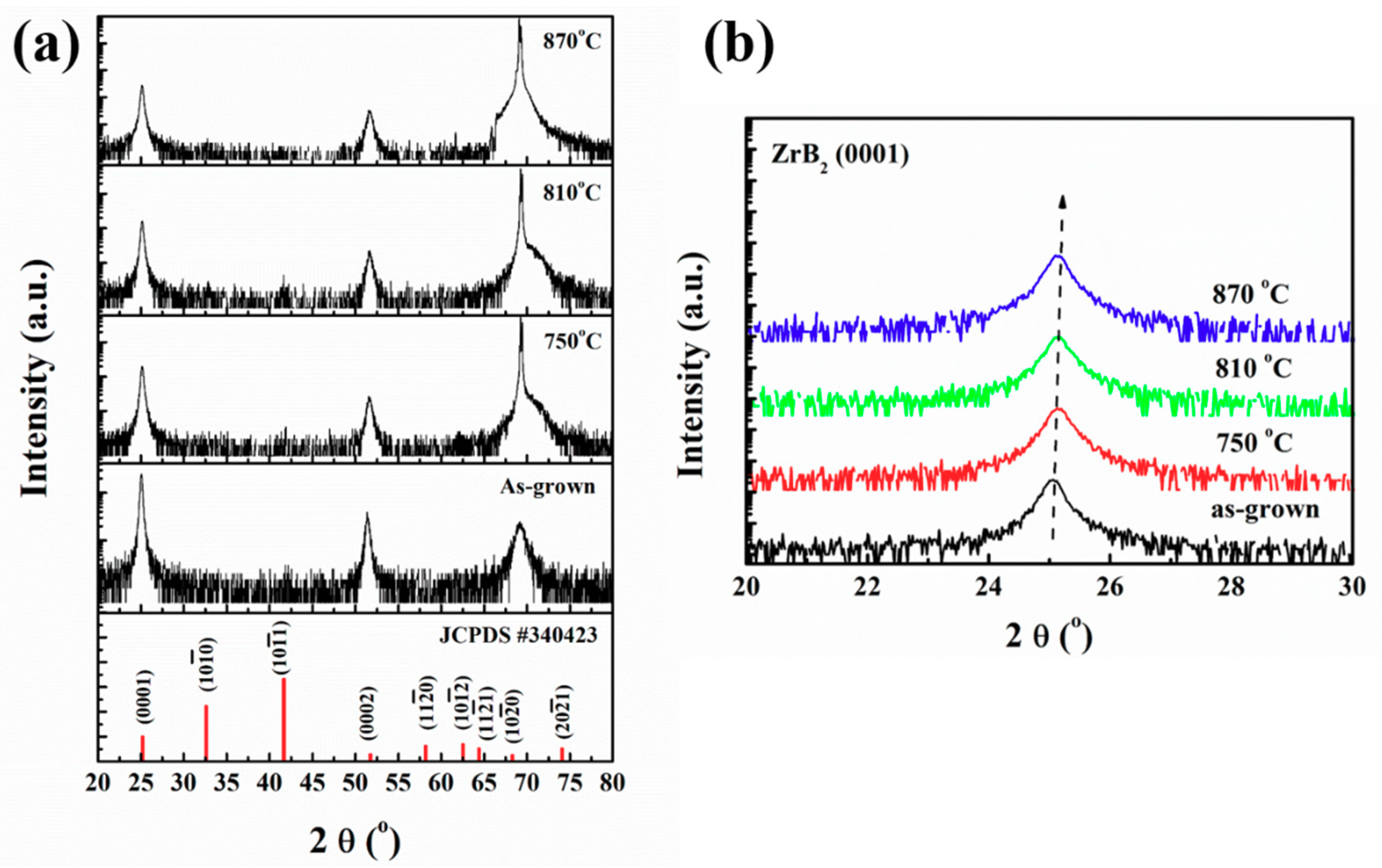
Figure 1a shows the XRD θ/2θ diffractograms of the all ZrB
2/Si(100) films, both as-grown and annealed at various temperatures. The pattern shows three peaks at 2θ = 25.16 ± 0.05°, 2θ = 51.68 ± 0.05° and 2θ = 69.26 ± 0.05° corresponding to ZrB
2(0001), ZrB
2(0002), and the Si(004) substrate in all ZrB
2 films, respectively, suggesting that they are preferentially oriented in the
c-axis direction. Thus, the XRD results indicate that the films possess a high
c-axis-orientated hexagonal crystal structure. These results are similar to those of Samuelsson et al., who reported ZrB
2 films deposited on a Si(100) substrate [
15].
Figure 1b exhibits shifts in the (0001) peak towards higher diffraction angles, which suggest that the films are in a state of tensile residual stress [
16]. This observed residual stress is due to energetic bombardment using Ar ions during sputtering. In addition, the
c-axis lattice parameters of ZrB
2 films were calculated from the (0001) lattice plane. The XRD pattern of the as-grown ZrB
2 film exhibits slightly shifted broad peaks, which indicate a large
c-axis lattice parameter. Moreover, the broad peaks reveal the poor crystallinity and residual stress of the film.
On the other hand, when the annealing temperature increased from 750 to 870 °C, the
c-axis lattice parameter of ZrB
2 films slightly decreased from 3.556 to 3.545 Å. The latter value is close to the
c-axis lattice constant of bulk ZrB
2, which was reported to be 3.530 Å, [
17] suggesting that the strain of ZrB
2 was almost relaxed after the annealing.
In addition, XRD profiles are used to measure the average crystallite size of the sample. For all the ZrB
2 films annealed at various temperatures, the crystallite size was calculated from XRD profiles from reflections with a strong intensity percentage by measuring the full width at half maximum (FWHM) of the relevant peaks. The Debye–Scherrer equation for calculating the crystallite size is given by Equation (1) [
18],
where λ is the X-ray wavelength of 1.54 Å, θ
B is the Bragg diffraction angle, and
B is the FWHM of the peak at θ
B. The calculated average crystallite sizes of the as-grown samples and those annealed at 750, 810, and 870 °C are 24.8, 25.3, 25.5 and 28.3 nm, respectively. Thus, the crystallite size of ZrB
2 slightly increased with the increasing annealing temperature, which can be understood as due to the merging process induced by thermal annealing. ZrB
2 films contain many dangling bonds related to the zirconium and boron defects at the grain boundaries. These defects are favorable to the merging process to form larger ZrB
2 grains with the increasing annealing temperature.
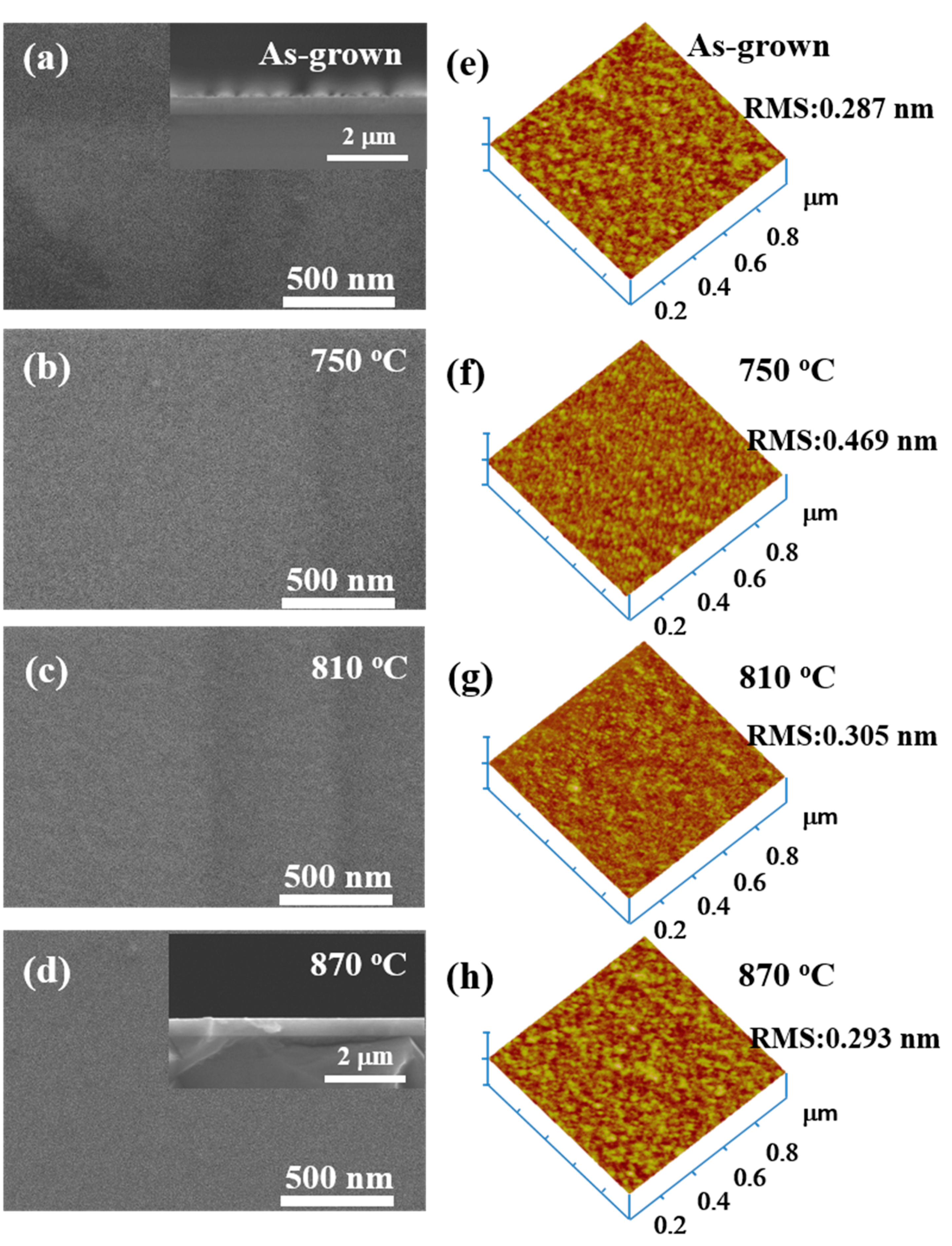
Figure 2 shows the SEM micrographs of the surface morphologies and AFM images of the surface roughness of all the ZrB
2 films. The surface morphology (including surface roughness, waviness and surface non-uniformities) of ZrB
2 films was clearly smooth. Additionally, all the ZrB
2 films exhibit fairly smooth surface morphologies, regardless of the annealing temperature. On the other hand, the cross-sectional images indicated that the as-grown ZrB
2 and annealed at 870 °C of ZrB
2 films were about 420 ± 10 nm thick. The ZrB
2 film still appears to be continuous without any delamination from the substrate and its thickness of 420 nm remains almost unchanged, implying that ZrB
2 is thermally and physically stable at high annealing temperatures. In addition, the ZrB
2 surfaces appear to be free of cracks after all the annealing treatments, indicating that the ZrB
2 films were capable of withstanding the thermal stresses produced using rapid cooling from high temperatures during the experiments. In addition, the surface roughness was analyzed by AFM. AFM topography presents some columnar-like grain growth. Moreover, the root-mean-square (RMS) surface roughness values were estimated from 1 × 1 μm
2 AFM tiny region scans, and the measurements indicate a smooth surface with an RMS surface roughness below 1 nm. The RMS surface roughness is 0.287 nm for the as-grown sample and 0.469, 0.305, and 0.293 nm for the samples annealed at 750, 810, and 870 °C, respectively. The surface profile of ZrB
2 is rather smooth, in agreement with the SEM observations.
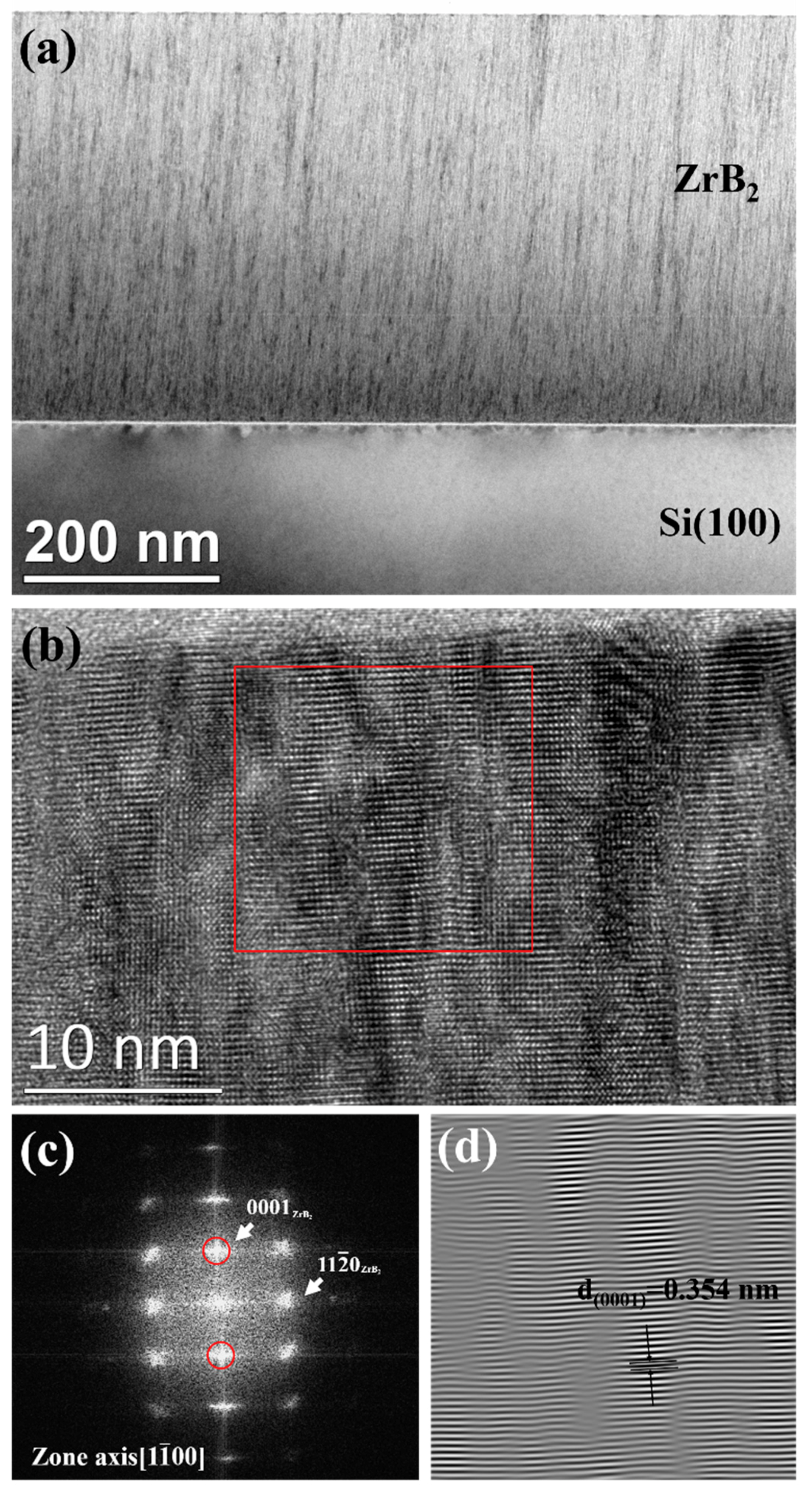
Figure 3a shows the cross-sectional bright-field TEM image of ZrB
2/Si(100) annealed at 870 °C. The cross-sectional transmission electron microscopy (XTEM, Philips Tecnai 20, Philips, Amsterdam, The Netherlands) images show that the ZrB
2 film grown on the Si(100) substrate is highly c-axis orientated from the film/substrate interface all the way to the film/vacuum interface. A smooth surface structure is clearly observed in the ZrB
2 film. In addition, the thickness of the ZrB
2 film was observed to be about 430 nm. In addition, a native oxide SiO
x layer was observed at the interface between the ZrB
2 film and the Si substrate.
Figure 3b shows the High-resolution cross-sectional transmission electron microscopy (HR-XTEM) image of the ZrB
2 film, wherein the ZrB
2 film columns appear to be shifted by half a unit cell, which constitute stacking mismatch boundaries. Some stacking faults are also observed. Additionally,
Figure 3c shows the Fast Fourier Transform (FFT) pattern calculated from
Figure 3b, which reveals the ZrB
2 film is characterized by the hexagonal structure. Individual diffraction spots can be identified as ZrB
2 reflections, indicating that ZrB
2 film exhibits a highly preferred orientation. In addition,
Figure 3d shows the Fourier-filtered image of the framed region in
Figure 3c, obtained by selecting the ±(0001)ZrB
2 spots in the SAD pattern. The
d(0001) spacing of ZrB
2 was determined from
Figure 3d to be approximately 0.354 nm, which is close to the bulk ZrB
2 value of 0.353 nm [
19].
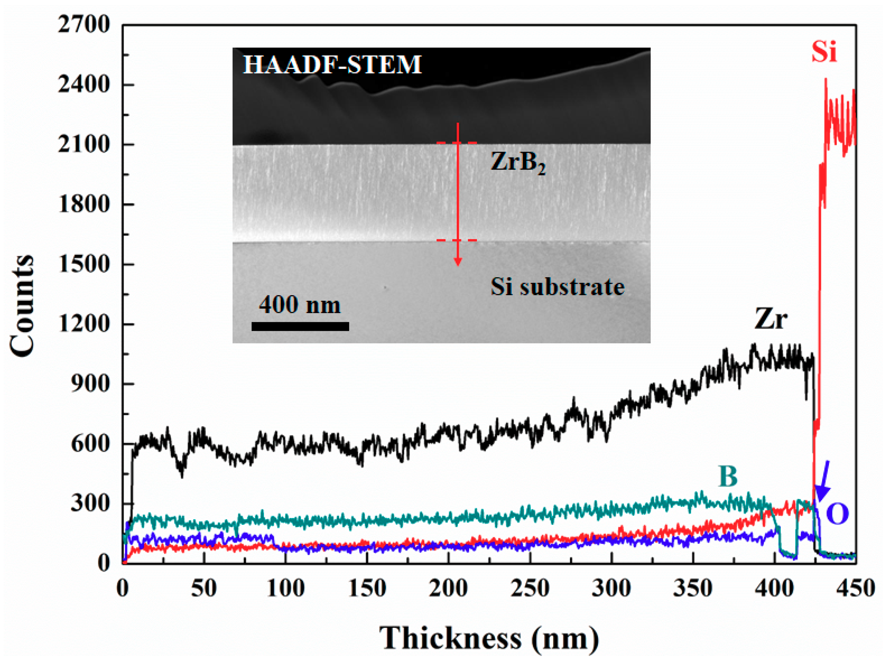
Figure 4 exhibits the TEM-Energy dispersive X-ray spectroscopy (EDS, Quantax, Bruker, Hamburg, Germany) line scan measured along the red line in the high-angle annular dark-field scanning transmission electron microscopy (HAADF-STEM, Tecnai G2 F20, FEI, Tokyo, Japan) image, which shows the ZrB
2 film and Si substrate. In the line scan results, the Zr profile shows a slightly higher concentration near the interface between the ZrB
2 film and the Si substrate. This result corresponds to the HAADF-STEM image. The average concentrations in the film regions are roughly estimated to be 55 ± 5 at % Zr and 25 ± 5 at % B. In addition, the EDS oxygen profiles display a slight peak in the oxygen concentration at the substrate–film interface (the red arrow in the inset of HAADF-STEM image). It is likely that a substantial part of this signal originates from sources other than the thin native oxide on the investigated Si(100) substrates, thus, indicating the presence of adsorbed oxygen-containing species on the substrate surfaces of the films deposited under these conditions.
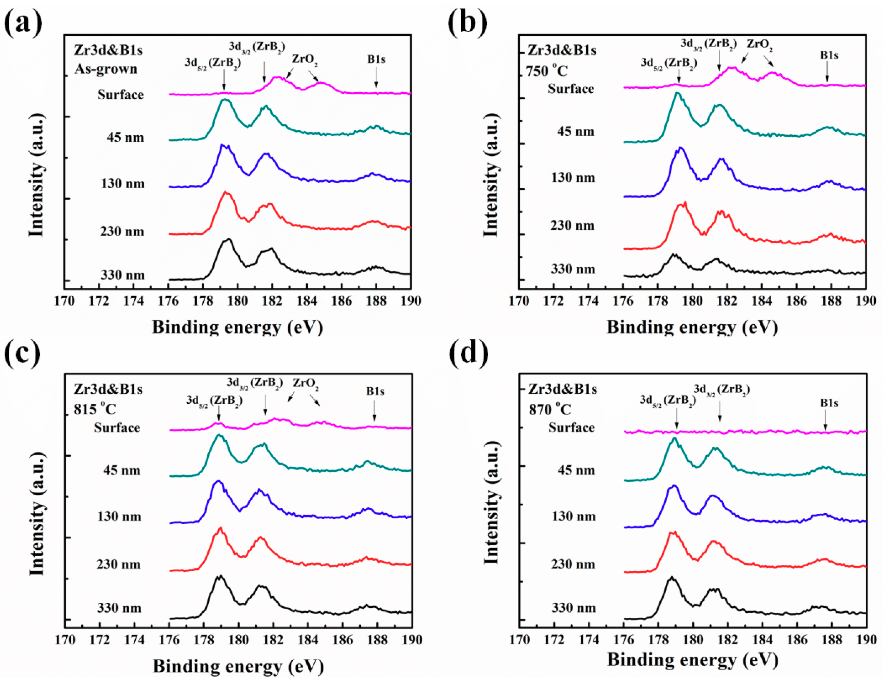
The chemical bonding structure and elemental composition of the ZrB
2 films were evaluated using XPS.
Figure 5 shows the Zr 3
d and B 1
s regions of the XPS spectra of all the samples, which indicate the presence of ZrB
2 in the depth profile. The spin–orbit energy difference between the 3
d5/2 and the 3
d3/2 components is around 2.38 ± 0.02 eV. The binding energy of Zr 3
d5/2 and Zr 3
d3/2 located at 179.28, 181.68 ± 0.1 eV are attributed to the Zr–B bonds in a ZrB
2 compound [
20]. The binding energy of Zr 3
d5/2 and Zr 3
d3/2 located at around 182.28 and 184.88 ± 0.1 eV are characteristic of the Zr–O bonds in oxide compounds [
21,
22]. Moreover, Zr–O was detected on the surface of films the as-grown film and those annealed at 750 and 810 °C. However, the Zr–O thin layer was undetected at the highest annealing temperature under vacuum. However, the Zr–O peak intensity decreases with the increasing annealing temperature. The estimated that of O atom adsorbed on the ZrB
2 surface forming a (2 × 2) super-structure but smaller than that of fully oxidized state Zr oxides [
23]. The B1s peak appears at 187.9 eV, which agrees with the reported B1s energy in ZrB
2 [
24]. These binding energies are in agreement with those determined for epitaxial ZrB
2 films deposited on 4H-SiC(0001) in Reference [
25], with values of 179.0, 181.3, and 188.0 eV, respectively. Furthermore, the binding energies are consistent with values for single-crystal bulk ZrB
2, i.e., 178.9, 181.3, and 187.9 eV, reported by Aizawa et al. [
26] and 179.0, 181.4, and 188.0 eV reported by Singh et al. [
27]. The XPS results suggest that the effective thickness of the native oxide layer on ZrB
2 decreased after annealing at 870 °C.


