The Effect of the Indium(III) Phthalocyanine Chloride Films on the Behavior of Flexible Devices of Flat and Disperse Heterojunction

 ,
,
Abstract
:1. Introduction
2. Materials and Methods
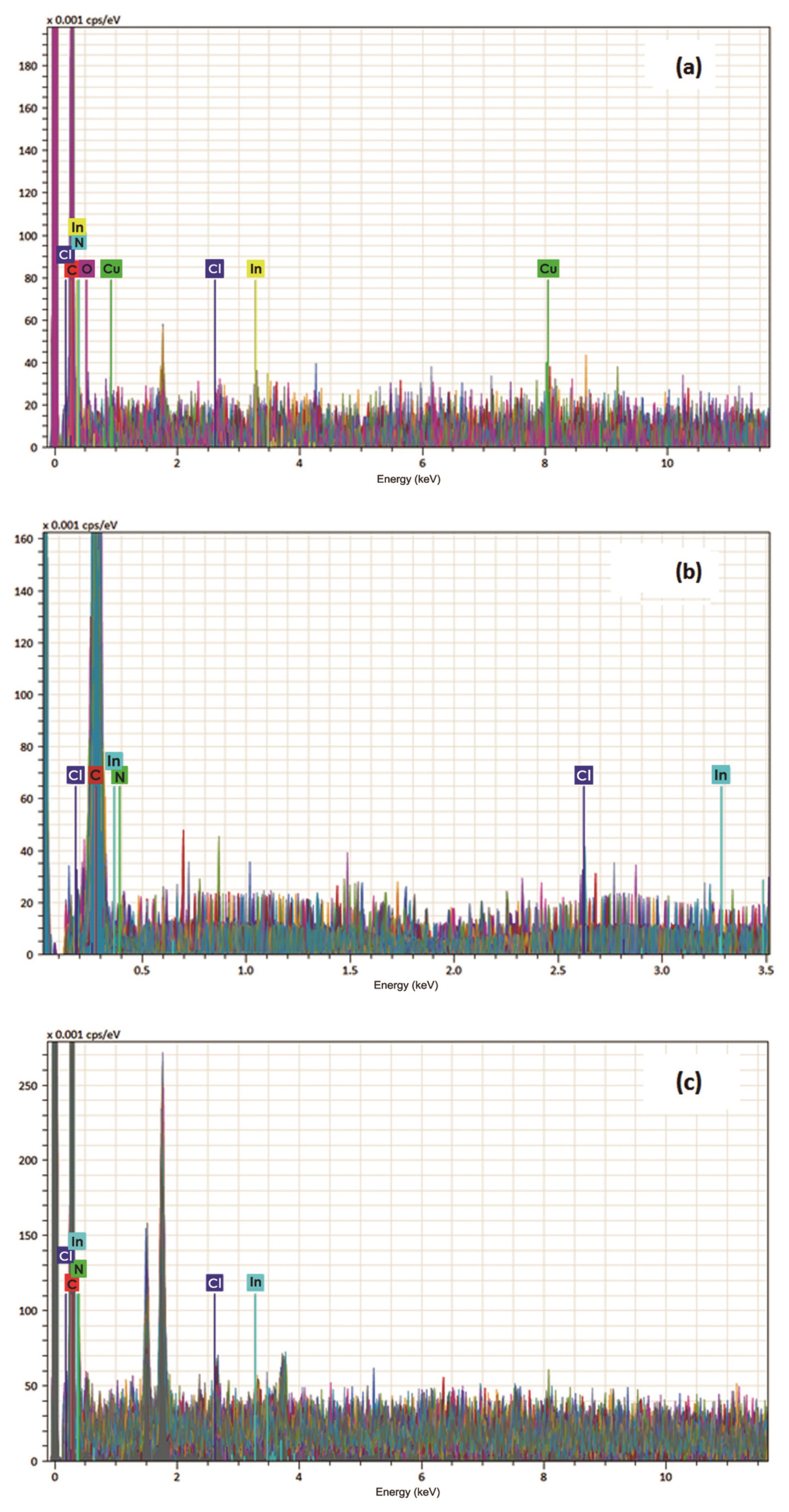
2.1. Characterization of Semiconductors
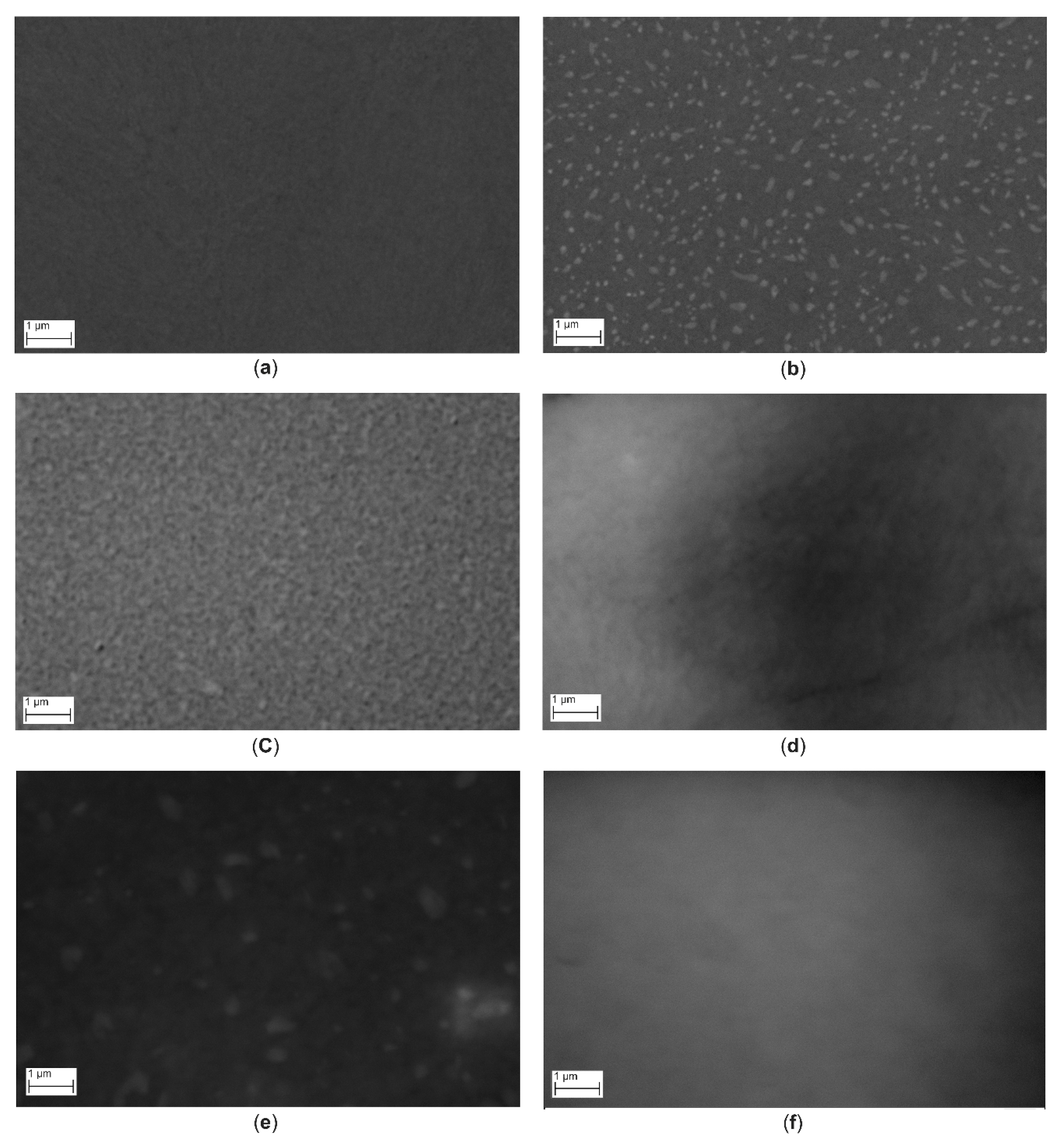
2.2. Film Deposition and Characterization
2.3. Device Assembling and Characterization
2.4. Theoretical Methods
3. Results and Discussion
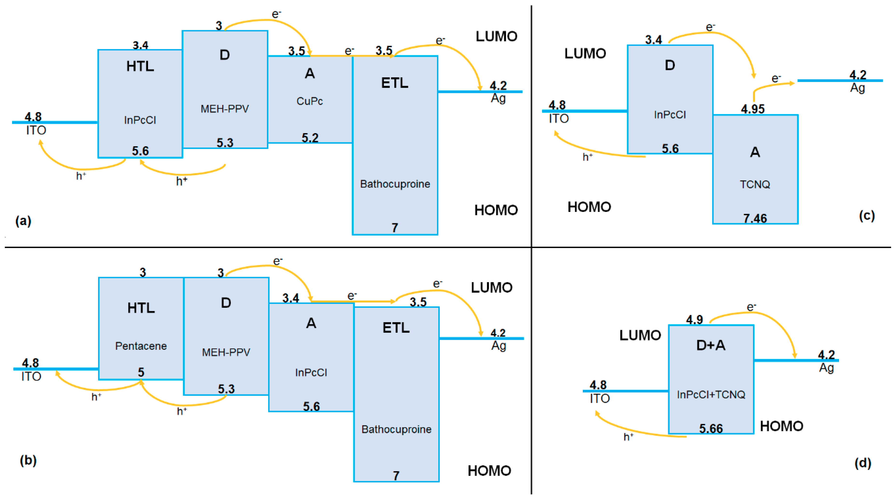
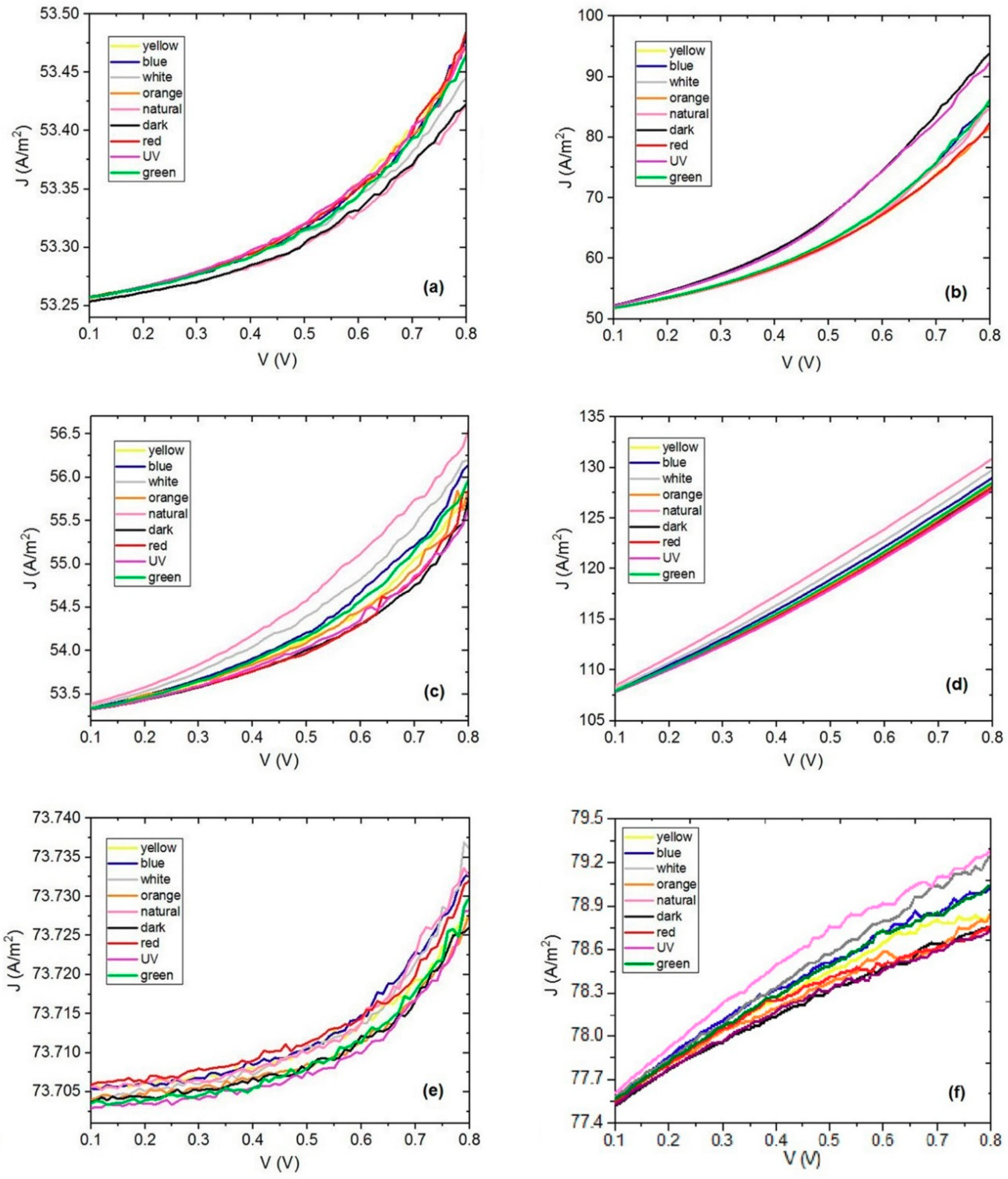
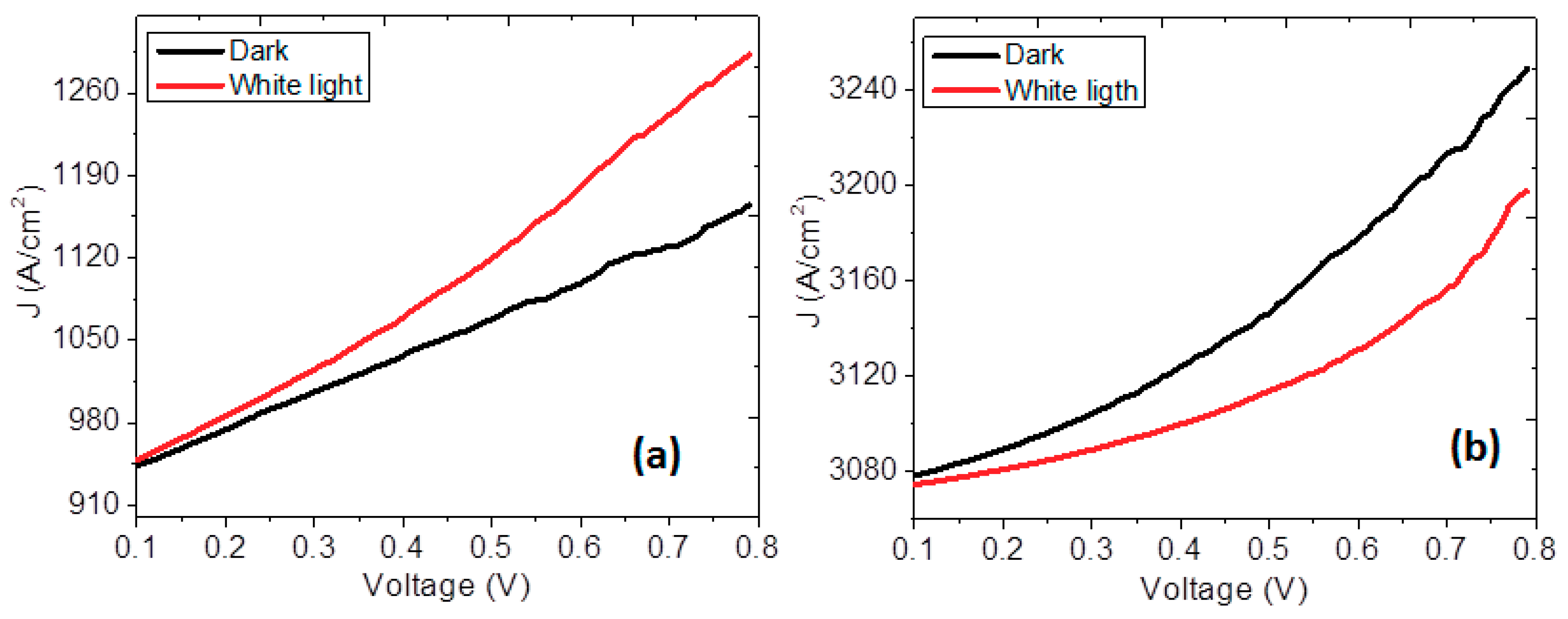
3.1. Manufacture and Characterization of FHJ Structures
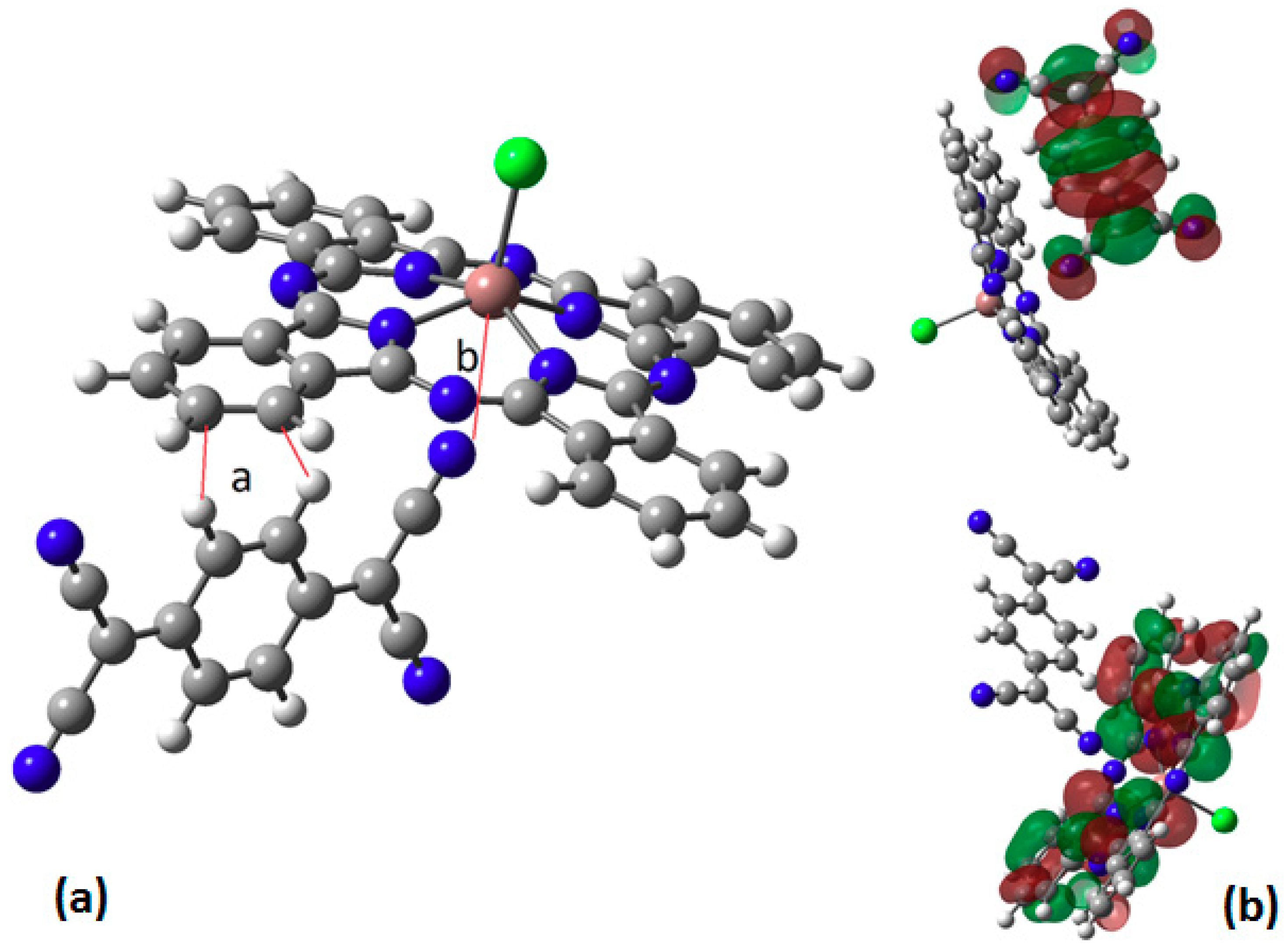
3.2. DFT Calculations and Characterization of BHJ structure
4. Conclusions
Author Contributions
Funding
Acknowledgments
Conflicts of Interest
References
- Hains, A.W.; Liang, Z.; Woodhouse, M.A.; Gregg, B.A. Molecular semiconductors in organic photovoltaic cells. Chem. Rev. 2010, 110, 6689–6735. [Google Scholar] [CrossRef] [PubMed]
- Pandey, A.K.; Nunzi, J.M. Efficient flexible and thermally stable pentacene/C60 small molecule based organic solar cells. Appl. Phys. Lett. 2006, 89, 213506. [Google Scholar] [CrossRef] [Green Version]
- Kushto, G.P.; Kim, W.; Kafafi, Z.H. Flexible organic photovoltaics using conducting polymer electrodes. Phys. Lett. 2005, 86, 093502. [Google Scholar] [CrossRef]
- Gu, G.; Burrows, P.E.; Venkatesh, S.; Forrest, S.R.; Thompson, M.E. Vacuum-deposited, nonpolymeric flexible organic light-emitting devices. Opt. Lett. 1997, 22, 172–174. [Google Scholar] [CrossRef]
- Cosseddu, P.; Lai, S.; Barbaro, M.; Bonfiglio, A. Ultra-low voltage, organic thin film transistors fabricated on plastic substrates by a highly reproducible process. Appl. Phys. Lett. 2012, 100, 093305. [Google Scholar] [CrossRef]
- Ahn, M.H.; Cho, E.S.; Kwon, S.J. Characteristics of ITO-resistive touch film deposited on a PET substrate by in-line DC magnetron sputtering. Vacuum 2013, 101, 221–227. [Google Scholar] [CrossRef]
- Machinaga, H.; Ueda, E.; Mizuike, A.; Takeda, Y.; Shimokita, K.; Miyazaki, T. Effects of annealing temperature on mechanical durability of indium-tin oxide film on polyethylene terephthalate substrate. Thin Solid Film. 2014, 559, 36–39. [Google Scholar] [CrossRef]
- Socol, M.; Preda, N.; Rasoga, O.; Breazu, C.; Stavarache, I.; Stanculescu, F.; Socol, G.; Gherendi, F.; Grumezescu, V.; Popescu-Pelin, G.; et al. Flexible heterostructures based on metal phthalocyanines thin films obtained by MAPLE. Appl. Surf. Scien. 2016, 374, 403–410. [Google Scholar] [CrossRef]
- Ponce Ortiz, R. Organic Semiconductors based on Oligotiofenos Tetracianosustituidos: Spectroscopic, Electrochemical and Theoretical Study. Ph.D. Thesis, University of Málaga, Málaga, Spain, 2008. [Google Scholar]
- Mirsafaei, M.; Fallahpour, A.H.; Lugli, P.; Rubahn, H.G.; Adam, J.; Madsen, M. The influence of electrical effects on device performance of organic solar cells with nano-structured electrodes. Sci. Rep. 2017, 7, 5300. [Google Scholar] [CrossRef] [PubMed]
- Zhao, H.; He, Z.; Zhang, X.; Zhang, Z.; Diyaf, Z.; Lind, A.H.N.; Liang, C.; Wilson, J.I.B. A preliminary investigation into hybrid photovoltaic cells with organic phthalocyanines and amorphous silicon heterojunction. J. Phys. D: Appl. Phys. 2015, 48, 19. [Google Scholar] [CrossRef]
- Bruder, I.; Schöneboom, J.; Dinnebier, R.; Ojala, A.; Schäfer, S.; Sens, R.; Erk, P.; Weis, J. What determines the performance of metal phthalocyanines (MPc, M = Zn, Cu, Ni, Fe) in organic heterojunction solar cells? A combined experimental and theoretical investigation. Org. Elec. 2010, 11, 377–387. [Google Scholar] [CrossRef]
- Osifeko, O.L.; Nyokong, T. Effects of symmetry and the number of positive charges on the photocatalytic activity of indium phthalocyanines when embedded in electrospun fibers. Inorg. Chim. Acta 2017, 458, 50–57. [Google Scholar] [CrossRef]
- Köksoy, M.A.; Köksoy, B.; Durmus¸, M.; Bulut, M. Preparation, characterization and photophysicochemical properties of novel tetra 7-(diethyl 2-methylmalonatoxy)-3-(p-oxyphenyl) coumarin-substituted zinc(II) and indium(III)chloride phthalocyanines. J. Organomet. Chem. 2016, 822, 125–134. [Google Scholar] [CrossRef]
- Sevim, A.M.; Yenilmez, H.Y.; Aydemir, M.; Koca, A.; Bayır, Z.A. Synthesis, electrochemical and spectroelectrochemical properties of novel phthalocyanine complexes of manganese, titanium and indium. Electrochim. Acta 2014, 137, 602–615. [Google Scholar] [CrossRef]
- Özceşmeci, I.; Gelir, A.; Gül, A. Synthesis and photophysical properties of indium(III) phthalocyanine derivatives. J. Lumin. 2014, 147, 141–146. [Google Scholar] [CrossRef]
- Hanack, M.; Dini, D.; Barthel, M.; Vagin, S. Conjugated macrocycles as active materials in nonlinear optical processes: optical limiting effect with phthalocyanines and related compounds. Chem. Rec. 2002, 2, 129–148. [Google Scholar] [CrossRef]
- Liu, Y.; Chen, Y.; Cai, L.; Wang, J.; Lin, Y.; Doyle, J.J.; Blau, J.W. Optical limiting properties of axially substituted indium phthalocyanines in the solid PMMA composite films. Mater. Chem. Phys. 2008, 107, 189–192. [Google Scholar] [CrossRef]
- Bankole, O.M.; Britton, J.; Nyokong, T. Photophysical and non-linear optical behavior of novel tetra alkynyl terminated indium phthalocyanines: Effects of the carbon chain length. Polyhedron 2015, 88, 73–80. [Google Scholar] [CrossRef]
- Becke, A.D. Density-functional exchange-energy approximation with correct asymptotic behavior. Phys. Rev. A 1998, 38, 3098–3100. [Google Scholar] [CrossRef]
- Perdew, J.P.; Wang, Y. Accurate and simple analytic representation of the electron-gas correlation energy. Phys. Rev. B 1992, 45, 13244–13249. [Google Scholar] [CrossRef]
- Frisch, M.J.; Trucks, G.W.; Schlegel, H.B.; Scuseria, G.E.; Robb, M.A.; Cheeseman, J.R.; Scalmani, G.; Barone, V.; Mennucci, B.; Petersson, G.A.; et al. Gaussian 09, Revision A.01; Gaussian, Inc.: Wallingford, CT, USA, 2009; Available online: https://gaussian.com/g09citation/ (accessed on 6 October 2019).
- García-Moreno, G. Organic Semiconductors Pi-Conjugated Based in Thiophene, Theoretical Study. Ph.D. Thesis, University of Jaen, Jaén, Spain, 2012. [Google Scholar]
- El-Nahass, M.M.; Farag, A.M.; Abd-El-Rahman, K.F.; Darwish, A.A.A. Dispersion studies and electronic transitions in nickel phthalocyanine thin films. Opt. Laser Technol. 2005, 37, 513–523. [Google Scholar] [CrossRef]
- El-Nahass, M.M.; Ammar, A.H.; Farag, A.A.M.; Atta, A.A.; El-Zaidia, E.F.M. Effect on heat treatment on morphological, structural and optical properties of CoMTPP thin films. Solid State Sci. 2011, 13, 596–600. [Google Scholar] [CrossRef]
- El-Nahass, M.M.; Sallam, M.; Ali, H.A.M. Optical properties of thermally evaporated metal-free phathalocyanine (H2Pc) thin films. Int. J. Mod. Phys. B 2005, 27, 4057–4071. [Google Scholar] [CrossRef]
- Regimol, C.C.; Menon, C.S. Effect of annealing and γ irradiation on tin phthalocyanine thin films. Mater. Sci. 2007, 25, 649–655. [Google Scholar]
- Novotny, M.; Bulir, J.; Bensalah-Ledoux, A.; Guy, S.; Fitl, P.; Vrnata, M.; Lancok, J.; Moine, B. Optical properties of zinc phthalocyanine thin films prepared by pulsed laser deposition. Appl. Phys. A 2014, 117, 377–381. [Google Scholar] [CrossRef]
- Tauc, J. Optical properties and electronic structure of amorphous Ge and Si. Mater. Res. Bull. 1968, 3, 37–46. [Google Scholar] [CrossRef]
- Mok, T.M.; O’Leary, S.K. The dependence of the Tauc and Cody optical gaps associated with hydrogenated amorphous silicon on the film thickness: αl Experimental limitations and the impact of curvature in the Tauc and Cody plots. J. Appl. Phys. 2007, 102, 113525. [Google Scholar] [CrossRef]
- Fox, M. Optical Properties of Solids. Ed Oxford University Press. Available online: https://pdfs.semanticscholar.org/23ff/f8d38a2c6566c35950412894bfc6fe5e82e3.pdf (accessed on 6 August 2019).
- Cody, G.D.; Brooks, B.G.; Abeles, B. Optical absorption above the optical gap of amorphous silicon hydride. Sol. Energy Mater. 1982, 8, 231–240. [Google Scholar] [CrossRef]
- Más-Montoya, M. Synthesis of New Heteroacene Systems and Study of Their Properties as Organic Semiconductors for Their Application in Molecular Electronics. Dissertation, University of Murcia, Spain, 2015. [Google Scholar]
- Örek, C.; Arslan, F.; Gündüz, B.; Kaygili, O.; Bulut, N. Comparison of experimental photonic and refractive index characteristics of the TBADN films with their theoretical counterparts. Chem. Phys. Lett. 2018, 696, 12–18. [Google Scholar] [CrossRef]


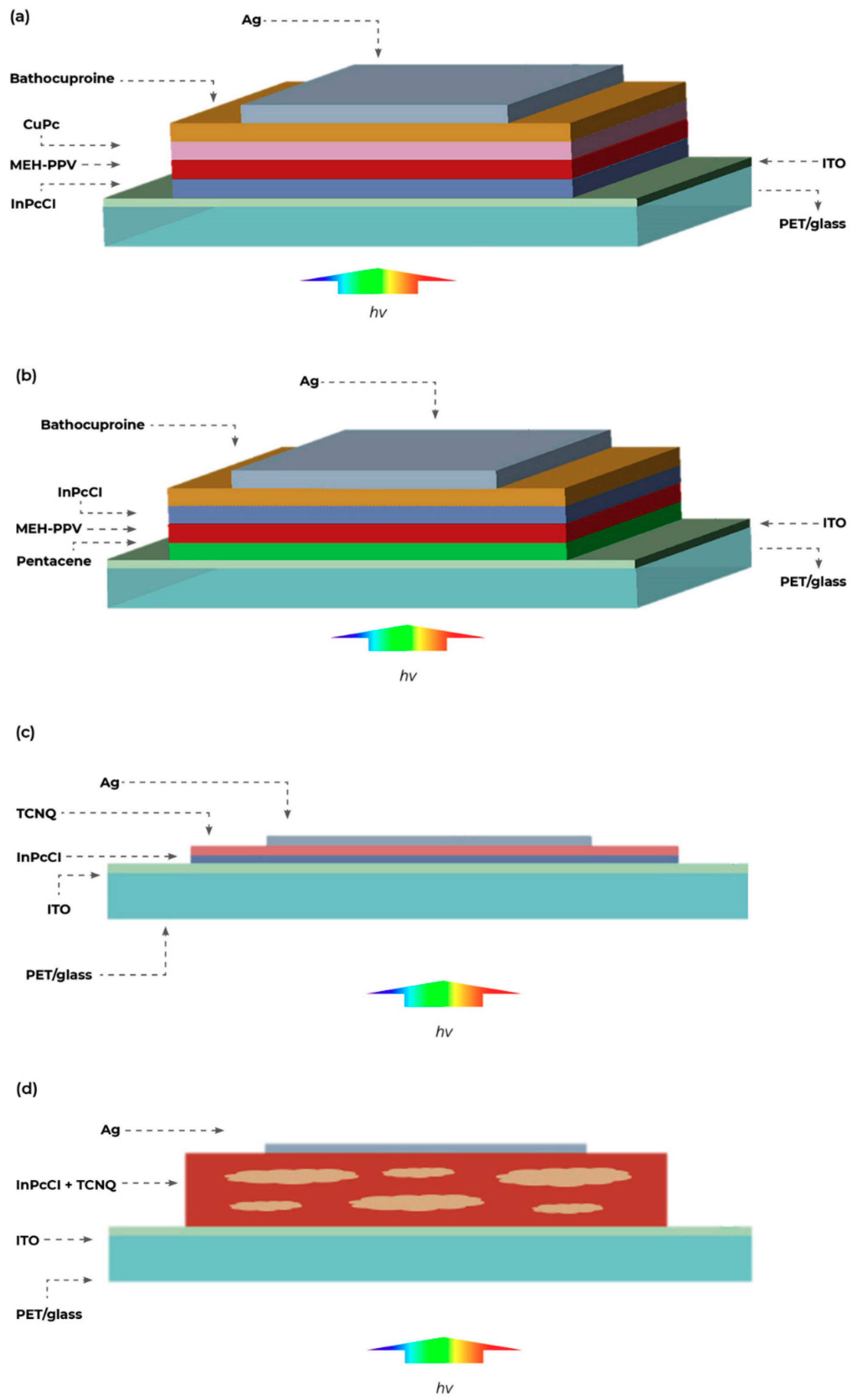
| Code | Type of Device | MSC | Structure | Function | Temperature mp (°C) |
|---|---|---|---|---|---|
| D1 D2 D3 | FHJ FHJ FHJ | In(III)PcCl |  | Hole Transport Layer (HTL) Electronic Acceptor Electronic Donor | >300 |
| D1, D2 | FHJ | MEH-PPV |  | Electronic Donor | 190–200 |
| D1 | FHJ | CuPc |  | Electronic Acceptor | 350 |
| D1, D2 | FHJ | Bathocuproine |  | Electrons Transport Layer (ETL) | 279 |
| D2 | FHJ | Pentacene |  | Hole Transport Layer (HTL) | 372 |
| D3 | FHJ | TCNQ |  | Electronic Acceptor | 287 |
| D4 | BHJ | InPcCl + TCNQ |  | Active Layer | >280 |
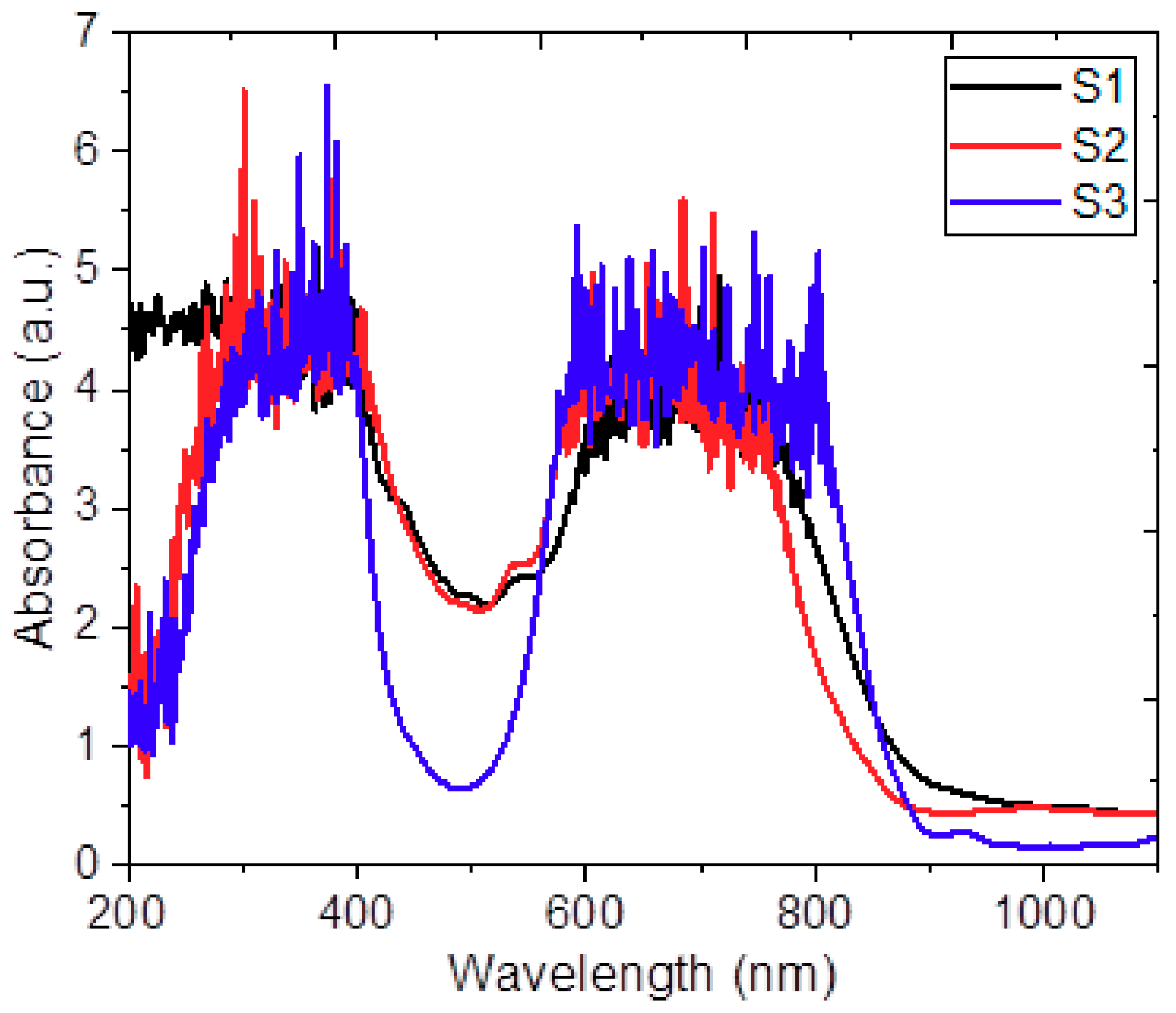
| Sample | Direct Tauc Bandgap (eV) | Indirect Tauc Bandgap (eV) | Direct Cody Bandgap (eV) | Indirect Cody Bandgap (eV) |
|---|---|---|---|---|
| S1 | 1.37 | 1.36 | 1.43 | 1.34 |
| S2 | 1.37 | 1.37 | 1.49 | 1.36 |
| S3 | 1.34 | 1.25 | 1.42 | 1.14 |
| Compound | HOMO (eV) | LUMO (eV) | DFT Bandgap (eV) | Direct Tauc Bandgap (eV) | Indirect Tauc Bandgap (eV) | Direct Cody Bandgap (eV) | Indirect Cody Bandgap (eV) |
|---|---|---|---|---|---|---|---|
| InPcCl + TCNQ | 5.66 | 4.90 | 0.761 | 1.06 | 1.10 | 1.20 | 1.03 |
© 2019 by the authors. Licensee MDPI, Basel, Switzerland. This article is an open access article distributed under the terms and conditions of the Creative Commons Attribution (CC BY) license (http://creativecommons.org/licenses/by/4.0/).
Share and Cite
Sánchez-Vergara, M.E.; Carrera-Téllez, R.; Smith-Ruiz, P.; Rios, C.; Salcedo, R. The Effect of the Indium(III) Phthalocyanine Chloride Films on the Behavior of Flexible Devices of Flat and Disperse Heterojunction. Coatings 2019, 9, 673. https://doi.org/10.3390/coatings9100673
Sánchez-Vergara ME, Carrera-Téllez R, Smith-Ruiz P, Rios C, Salcedo R. The Effect of the Indium(III) Phthalocyanine Chloride Films on the Behavior of Flexible Devices of Flat and Disperse Heterojunction. Coatings. 2019; 9(10):673. https://doi.org/10.3390/coatings9100673
Chicago/Turabian StyleSánchez-Vergara, María Elena, Raquel Carrera-Téllez, Paulina Smith-Ruiz, Citlalli Rios, and Roberto Salcedo. 2019. "The Effect of the Indium(III) Phthalocyanine Chloride Films on the Behavior of Flexible Devices of Flat and Disperse Heterojunction" Coatings 9, no. 10: 673. https://doi.org/10.3390/coatings9100673