
Effect of Photoanode Process Sequence on Efficiency of Dye-Sensitized Solar Cells


Abstract
:1. Introduction
2. Materials and Methods
2.1. Materials
2.2. Fabrication
2.2.1. Substrate Cleaning
2.2.2. TiO2 Paste Preparation
2.2.3. N3 Dye Preparation
2.2.4. Electrolyte Preparation
2.2.5. Photoanode Preparation
2.2.6. Counter Electrode Preparation
2.2.7. DSSC Device Encapsulation
2.3. Characterization
3. Results and Discussions
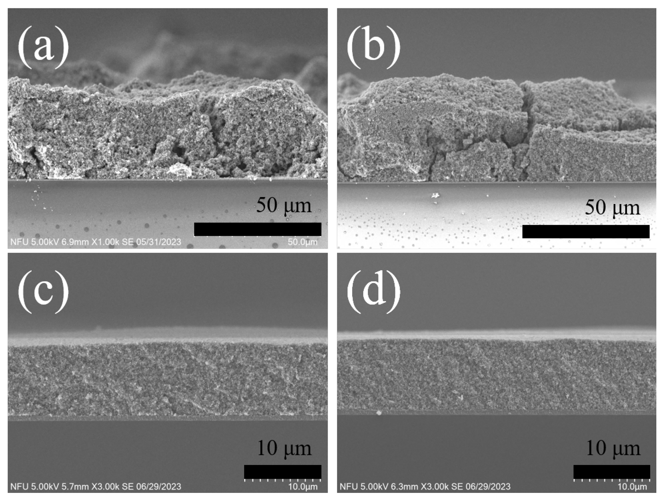
3.1. SEM Analysis
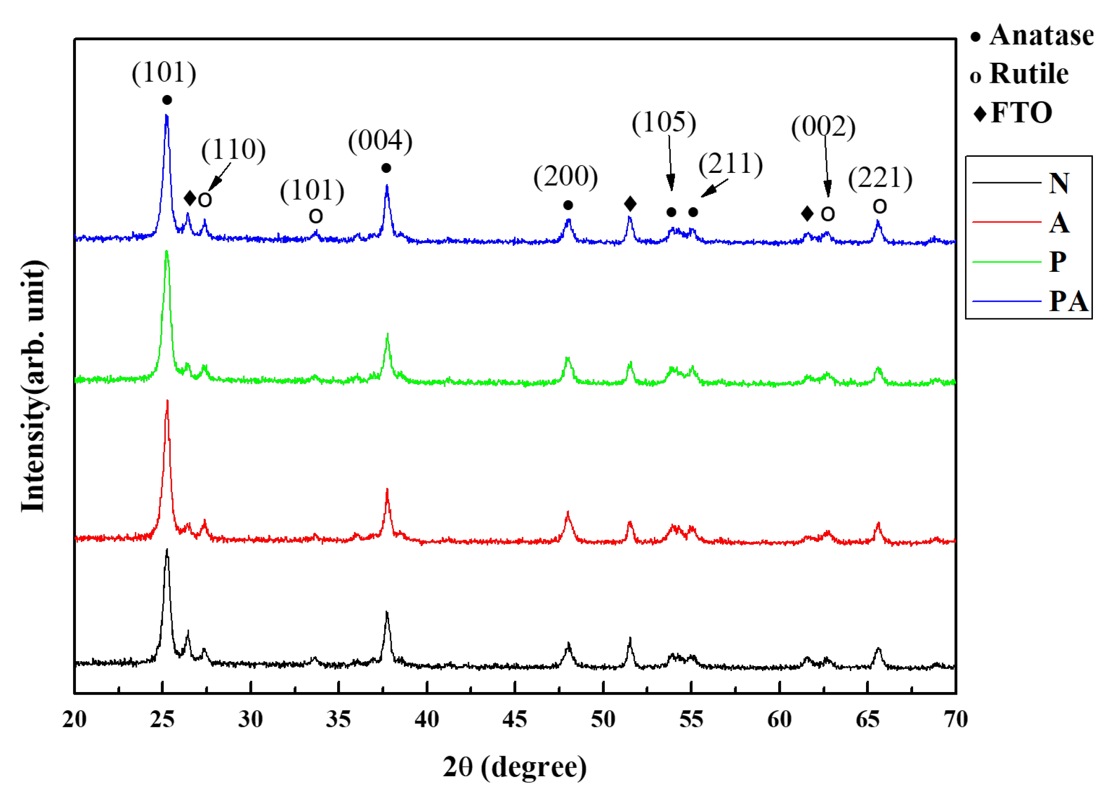
3.2. XRD Analysis
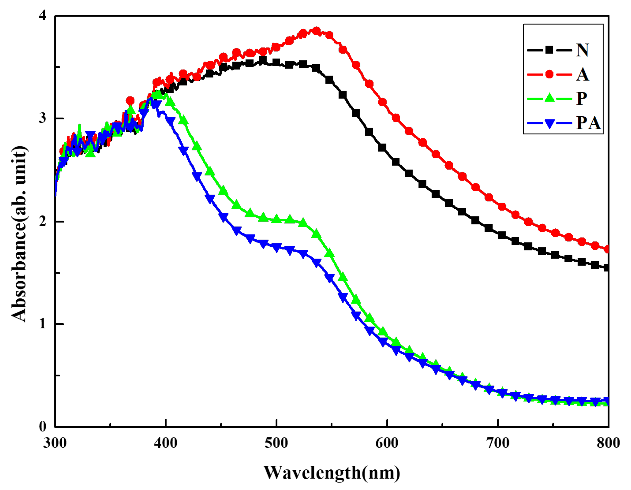
3.3. UV-Vis Analysis
3.4. EIS Characteristics
3.5. J-V Characteristics
4. Conclusions
Author Contributions
Funding
Institutional Review Board Statement
Informed Consent Statement
Data Availability Statement
Conflicts of Interest
References
- Wang, Q.; Guo, J.; Li, R.; Jiang, X.T. Exploring the role of nuclear energy in the energy transition: A comparative perspective of the effects of coal, oil, natural gas, renewable energy, and nuclear power on economic growth and carbon emissions. Environ. Res. 2023, 221, 115290. [Google Scholar] [CrossRef]
- Karim, N.A.; Mehmood, U.; Zahid, H.F.; Asif, T. Nanostructured photoanode and counter electrode materials for efficient DSSCs. Sol. Energy 2019, 185, 165–188. [Google Scholar] [CrossRef]
- Ito, S.; Murakami, T.N.; Comte, P.; Liska, P.; Grätzel, C.; Nazeeruddin, M.K.; Grätzel, M. Fabrication of thin film dye sensitized solar cells with solar to electric power conversion efficiency over 10%. Thin Solid Film. 2008, 516, 4613–4619. [Google Scholar] [CrossRef]
- Meen, T.H.; Tsai, J.K.; Tu, Y.S.; Wu, T.C.; Hsu, W.D.; Chang, S.-J. Optimization of the dye-sensitized solar cell performance by mechanical compression. Nanoscale Res. Lett. 2014, 9, 523. [Google Scholar] [CrossRef] [PubMed]
- Tsai, J.K.; Hsu, W.D.; Wu, T.C.; Meen, T.H.; Chong, W.J. Effect of compressed TiO2 nanoparticle thin film thickness on the performance of DSSCs. Nanoscale Res. Lett. 2013, 8, 459. [Google Scholar] [CrossRef] [PubMed]
- Cao, D.; Wang, A.; Yu, X.; Yin, H.; Zhang, J.; Mi, B. Room-temperature preparation of TiO2/graphene composite photoanodes for efficient dye-sensitized solar cells. J. Colloid Interface Sci. 2021, 586, 326–334. [Google Scholar] [CrossRef] [PubMed]
- Dittrich, T.; Ofir, A.; Tirosh, S.; Grinis, L.; Zaban, A. Influence of the porosity on diffusion and lifetime in porous TiO2 layers. Appl. Phys. Lett. 2006, 88, 182110. [Google Scholar] [CrossRef]
- Ahmad, M.S.; Pandey, A.K.; Abd Rahim, N. Advancements in the development of TiO2 photoanodes and its fabrication methods for dye-sensitized solar cell (DSSC) applications. A review. Renew. Sustain. Energy Rev. 2017, 77, 89–108. [Google Scholar] [CrossRef]
- Liu, J.; Li, Y.; Arumugam, S.; Tudor, J.; Beeby, S. Investigation of low temperature processed titanium dioxide (TiO2) films for printed dye-sensitized solar cells (DSSCs) for large area flexible applications. Mater. Today Proc. 2018, 5, 13846–13854. [Google Scholar] [CrossRef]
- Husain, A.; Hasan, W.W. Transparent solar cell using spin coating and screen printing. Pertanika J. Sci. Technol. 2017, 25, 225–233. [Google Scholar]
- Tsai, J.K.; Tu, Y.S. Fabrication of polymeric anti-reflection film manufactured by anodic aluminum oxide template on dye-sensitized solar cells. Materials 2017, 10, 296. [Google Scholar] [CrossRef]
- Liu, Y.; Lin, Y.; Wei, Y.; Liu, C. Formation of carriers in Ti-oxide thin films by substitution reactions. J. Appl. Phys. 2012, 111, 043103. [Google Scholar] [CrossRef]
- Zhang, S.; Zhang, X.; Sun, Y.; Zhou, W.; Cao, W.; Cheng, D. Investigation of the annealing treatment on the performance of TiO2 photoanode. Int. J. Hydrogen Energy 2023, 48, 29996–30005. [Google Scholar] [CrossRef]
- Phadke, S.; Du Pasquier, A.; Birnie, D.P., III. Enhanced electron transport through template-derived pore channels in dye-sensitized solar cells. J. Phys. Chem. C 2011, 115, 18342–18347. [Google Scholar] [CrossRef]
- Wu, T.C.; Huang, W.M.; Meen, T.H.; Tsai, J.K. Performance improvement of dye-sensitized solar cells with pressed TiO2 nanoparticles layer. Coatings 2023, 13, 907. [Google Scholar] [CrossRef]
- Kim, M.H.; Kwon, Y.U. Semiconductor CdO as a blocking layer material on DSSC electrode: Mechanism and application. J. Phys. Chem. C 2009, 113, 17176–17182. [Google Scholar] [CrossRef]
- Wang, J.; Wang, J.; Ding, J.; Wei, Y.; Zhang, J. Preparation of ZnO compact layer using vacuum ultraviolet for dye-sensitized solar cells. Solid State Sci. 2022, 127, 106860. [Google Scholar] [CrossRef]
- Jadhav, V.S.; Bhande, S.S.; Tehare, K.K.; Gaikwad, S.L.; Mane, R.S. Significance of compact layers on DSSCs performance of chemically deposited TiO2-based dye-sensitized solar cells. Int. J. Eng. Sci. 2015, 4, 30–34. [Google Scholar]
- Hanaor, D.A.; Sorrell, C.C. Review of the anatase to rutile phase transformation. J. Mater. Sci. 2011, 46, 855–874. [Google Scholar] [CrossRef]
- Li, J.; Zhang, H.; Wang, W.; Qian, Y.; Li, Z. Improved performance of dye-sensitized solar cell based on TiO2 photoanode with FTO glass and film both treated by TiCl4. Phys. B Condens. Matter 2016, 500, 48–52. [Google Scholar] [CrossRef]
- Omar, A.; Abdullah, H. Electron transport analysis in zinc oxide-based dye-sensitized solar cells: A review. Renew. Sustain. Energy Rev. 2014, 31, 149–157. [Google Scholar] [CrossRef]


| Sample | RS (Ω) | RPT (Ω) | RK (Ω) | RD (Ω) | Keff (s−1) | τeff (s) |
|---|---|---|---|---|---|---|
| N | 13.72 | N/A | 122.45 | 10.62 | 106.61 | 1.493 |
| A | 16.79 | 3.38 | 13.85 | 4.06 | 19.37 | 8.217 |
| P | 16.20 | 5.48 | 14.91 | 6.33 | 32.77 | 4.856 |
| PA | 12.96 | 3.26 | 14.82 | 8.42 | 19.37 | 8.217 |
| Sample | VOC (V) | JSC (mA/cm2) | Fill Factor (%) | PCE (%) |
|---|---|---|---|---|
| N | 0.77 | 1.91 | 69.22 | 1.01 |
| A | 0.73 | 9.44 | 67.55 | 4.67 |
| P | 0.72 | 6.36 | 71.46 | 3.29 |
| PA | 0.73 | 10.27 | 63.17 | 4.73 |
Disclaimer/Publisher’s Note: The statements, opinions and data contained in all publications are solely those of the individual author(s) and contributor(s) and not of MDPI and/or the editor(s). MDPI and/or the editor(s) disclaim responsibility for any injury to people or property resulting from any ideas, methods, instructions or products referred to in the content. |
© 2024 by the authors. Licensee MDPI, Basel, Switzerland. This article is an open access article distributed under the terms and conditions of the Creative Commons Attribution (CC BY) license (https://creativecommons.org/licenses/by/4.0/).
Share and Cite
Wu, T.-C.; Huang, W.-M.; Tsai, J.-K.; Chang, C.-E.; Meen, T.-H. Effect of Photoanode Process Sequence on Efficiency of Dye-Sensitized Solar Cells. Coatings 2024, 14, 304. https://doi.org/10.3390/coatings14030304
Wu T-C, Huang W-M, Tsai J-K, Chang C-E, Meen T-H. Effect of Photoanode Process Sequence on Efficiency of Dye-Sensitized Solar Cells. Coatings. 2024; 14(3):304. https://doi.org/10.3390/coatings14030304
Chicago/Turabian StyleWu, Tian-Chiuan, Wei-Ming Huang, Jenn-Kai Tsai, Cheng-En Chang, and Teen-Hang Meen. 2024. "Effect of Photoanode Process Sequence on Efficiency of Dye-Sensitized Solar Cells" Coatings 14, no. 3: 304. https://doi.org/10.3390/coatings14030304