
Wide-Spectrum Antireflective Properties of Germanium by Femtosecond Laser Raster-Type In Situ Repetitive Direct Writing Technique

Abstract
:1. Introduction
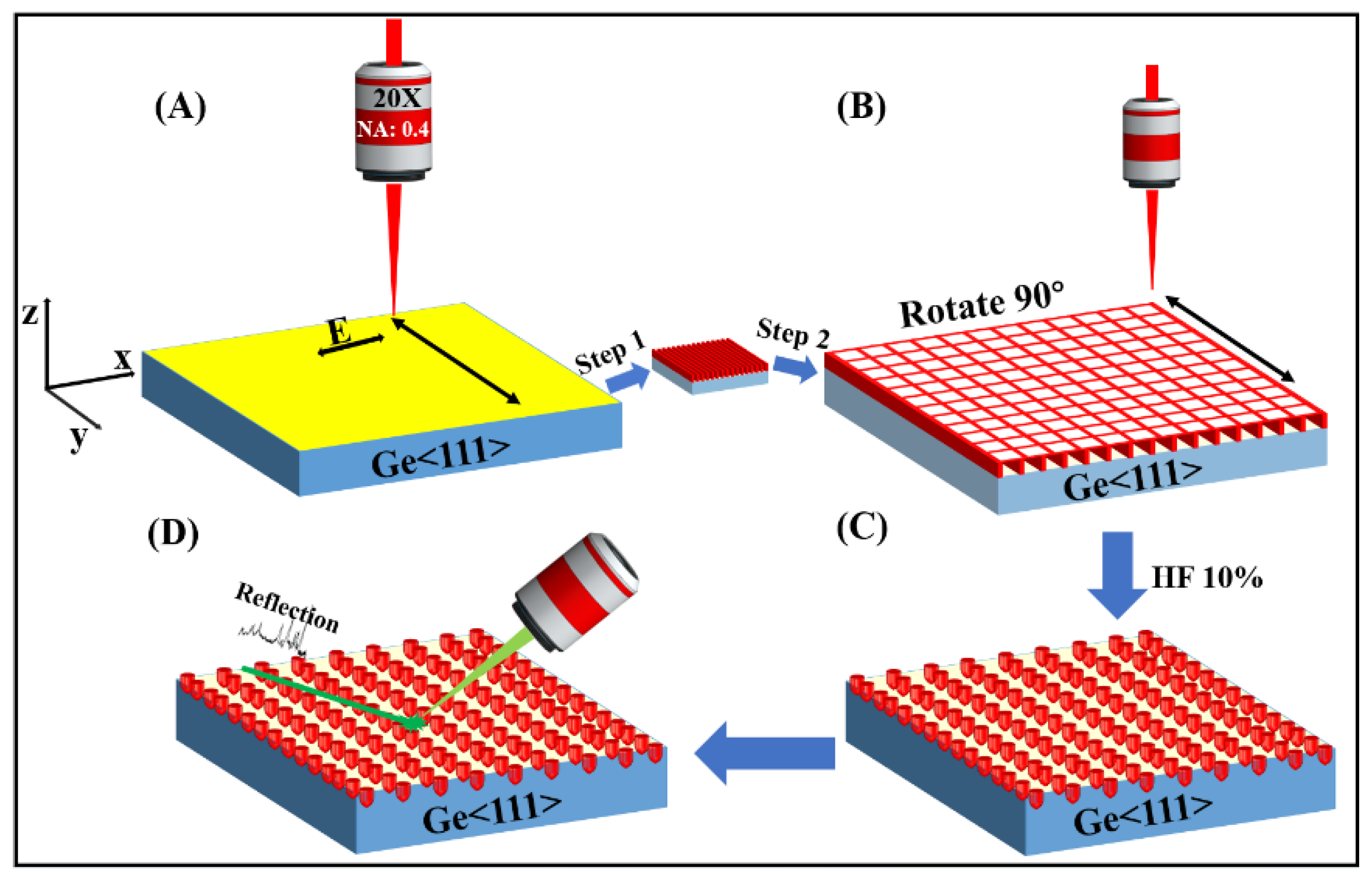
2. Experimental
3. Results and Discussion
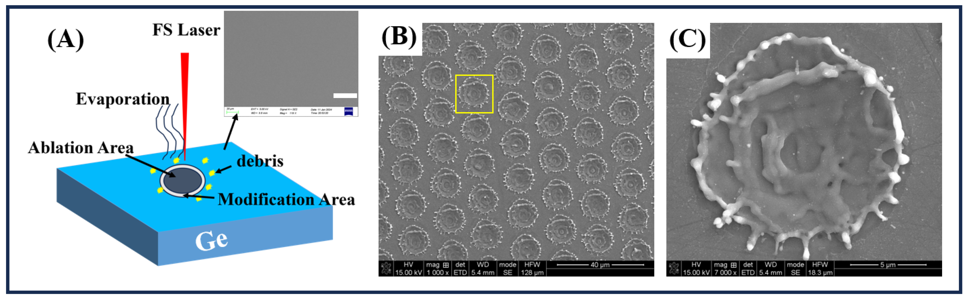
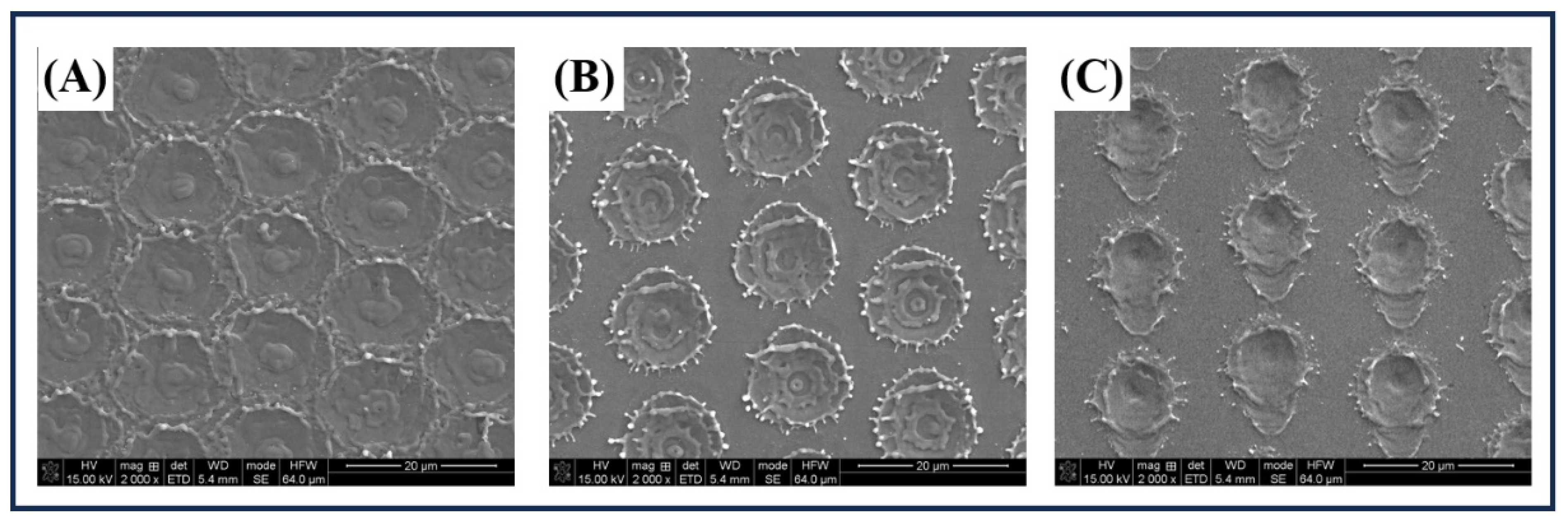
3.1. Ablative Morphology of Mono-Pulse Femtosecond Laser
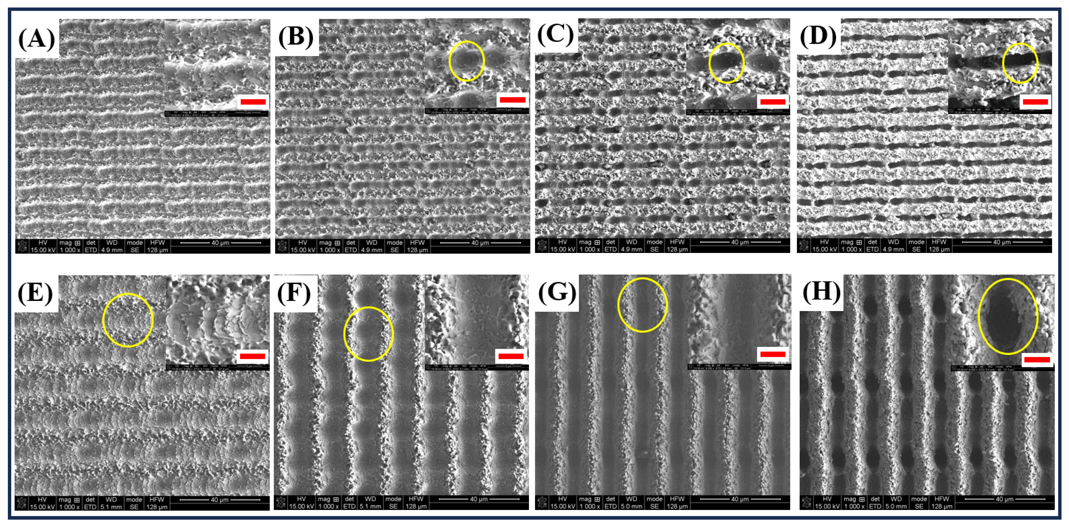
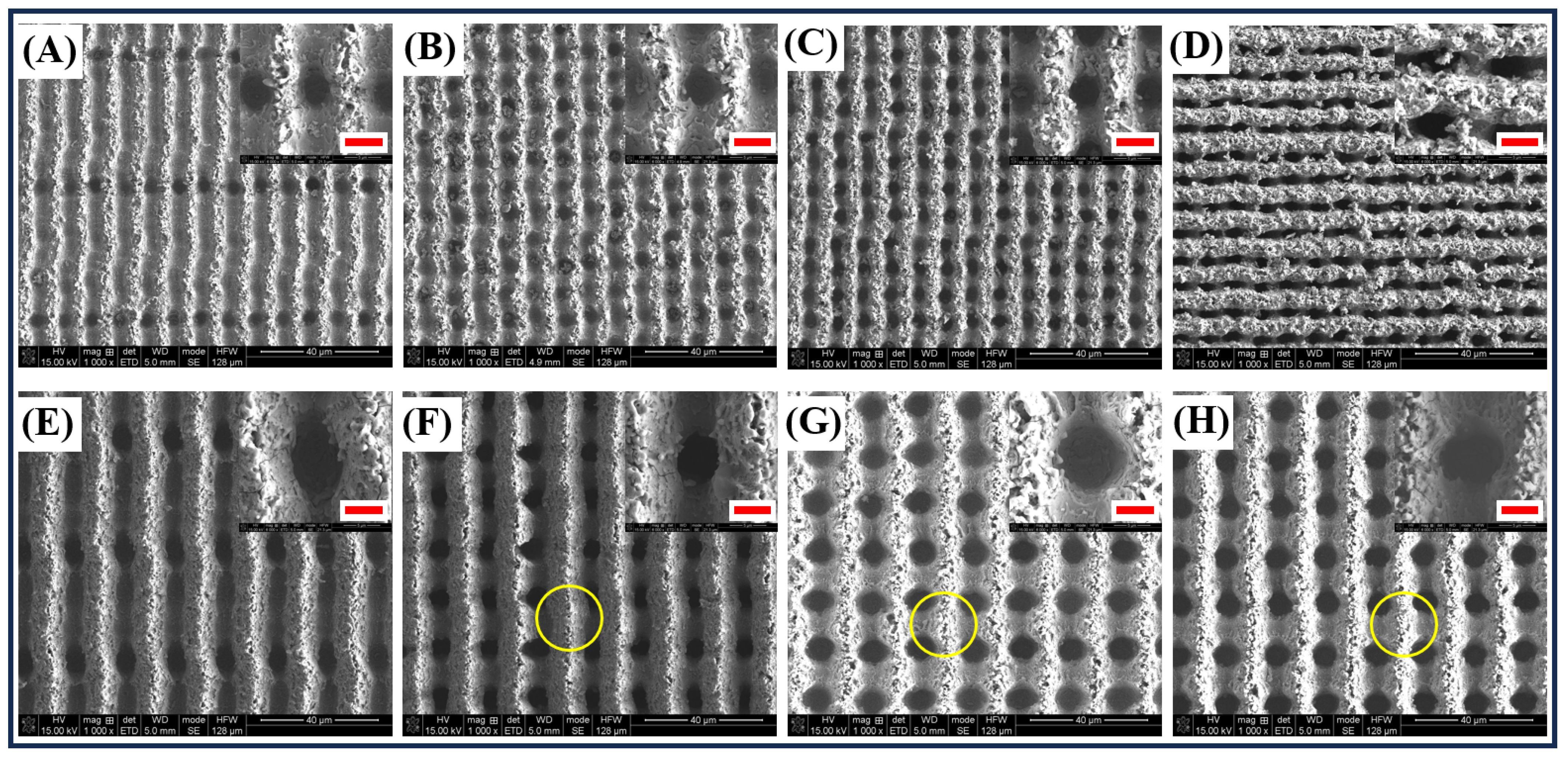
3.2. Raster-Type In Situ Repeat Direct Writing Technology
3.3. Orthogonal Laser Direct Writing
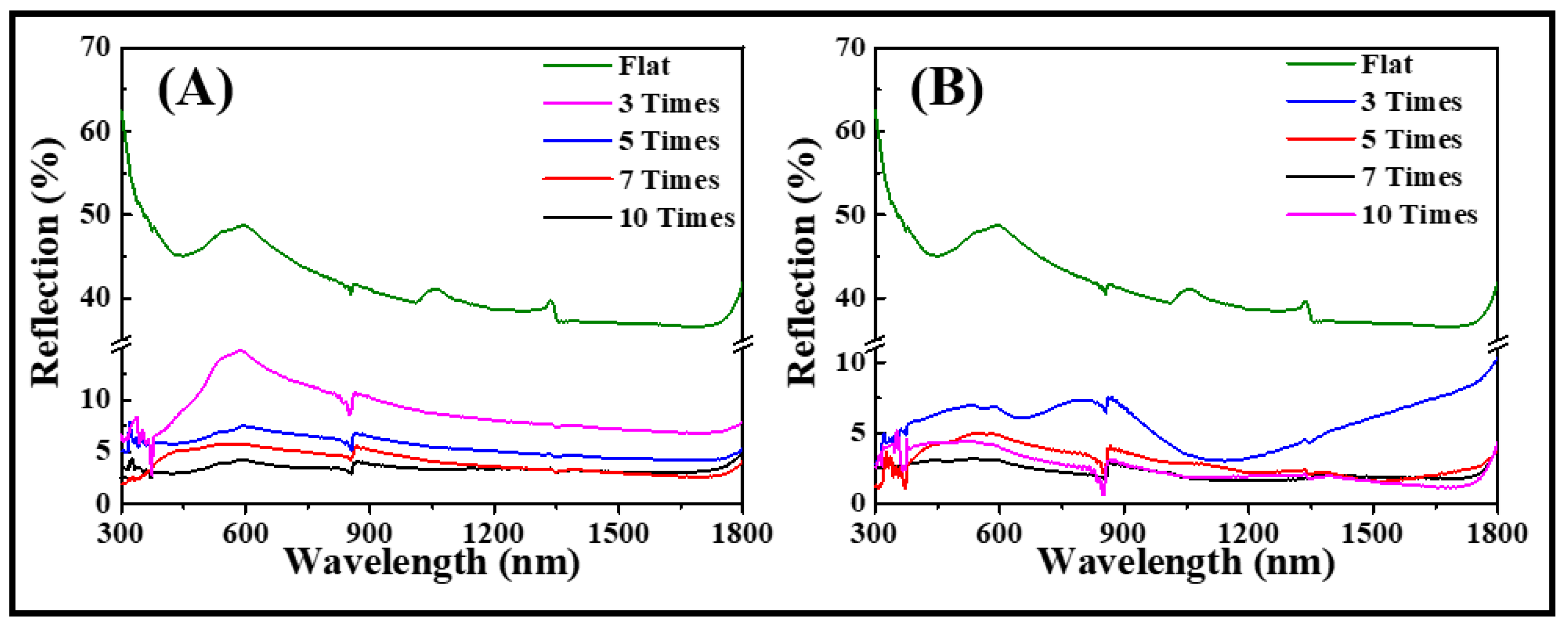
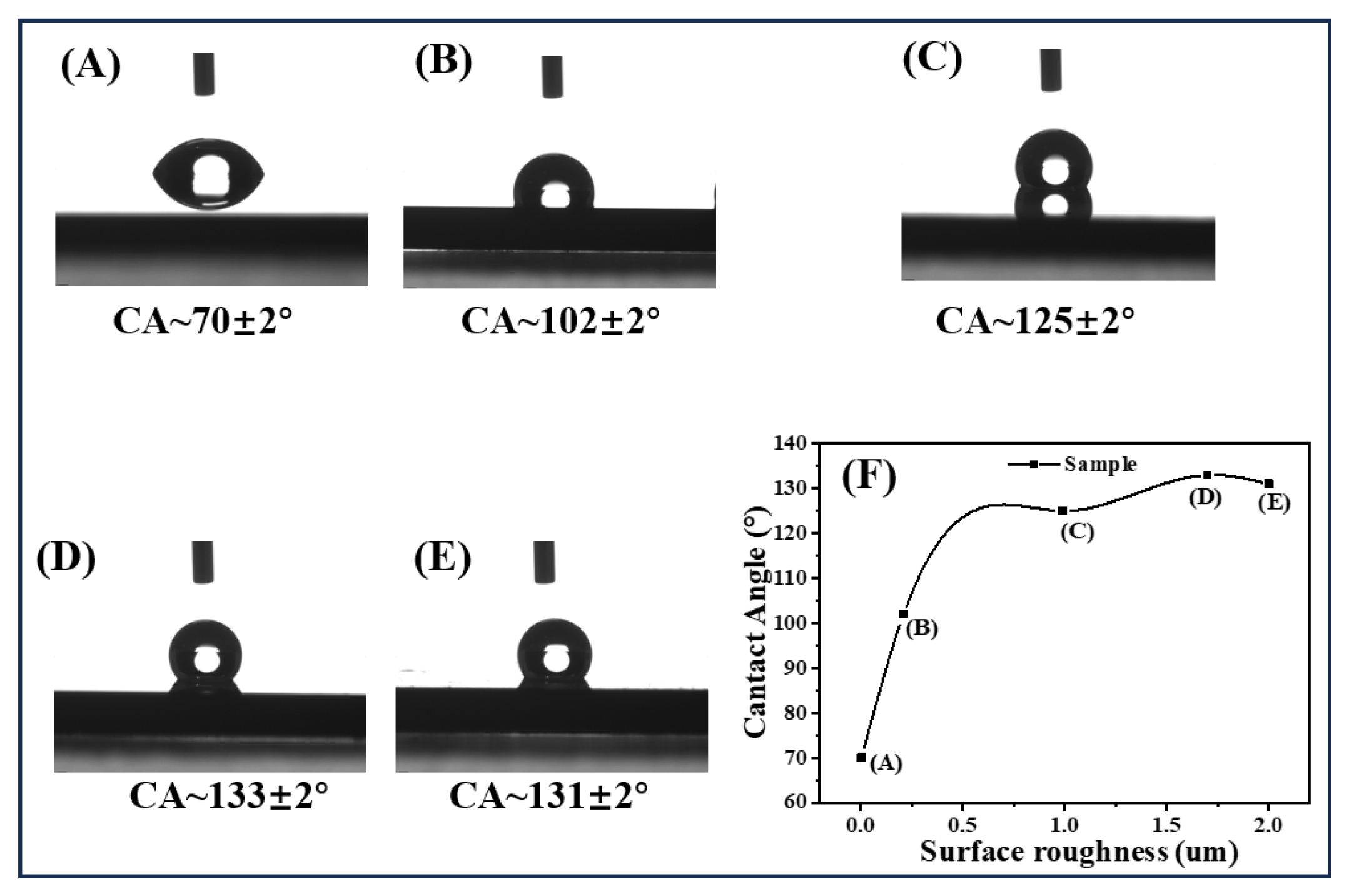
3.4. Optical and Hydrophilic Properties
4. Conclusions
Author Contributions
Funding
Institutional Review Board Statement
Informed Consent Statement
Data Availability Statement
Conflicts of Interest
References
- Jun, J.; Kim, H.; Choi, H.-J.; Lee, T.-W.; Ju, S.; Baik, J.M.; Lee, H. A Large-Area Fabrication of Moth-Eye Patterned Au/TiO2 Gap-Plasmon Structure and Its Application to Plasmonic Solar Water Splitting. Sol. Energy Mater. Sol. Cells 2019, 201, 110033. [Google Scholar] [CrossRef]
- Xie, H.; Huang, H.-X.; Peng, Y.-J. Rapid Fabrication of Bio-Inspired Nanostructure with Hydrophobicity and Antireflectivity on Polystyrene Surface Replicating from Cicada Wings. Nanoscale 2017, 9, 11951–11958. [Google Scholar] [CrossRef] [PubMed]
- Abdelmalek, A.; Kotsedi, L.; Bedrane, Z.; Amara, E.-H.; Girolami, M.; Maaza, M. Optical and Thermal Behavior of Germanium Thin Films under Femtosecond Laser Irradiation. Nanomaterials 2022, 12, 3786. [Google Scholar] [CrossRef] [PubMed]
- Ali, A.; Piatkowski, P.A.; Alawadhi, H.; Alnaser, A.S. Reducing the Cut-In Voltage of a Silicon Carbide/p-Silicon Heterojunction Diode Using Femtosecond Laser Ablation. ACS Appl. Electron. Mater. 2022, 4, 6076–6086. [Google Scholar] [CrossRef]
- Chowdhury, D.; Mondal, S.; Secchi, M.; Giordano, M.C.; Vanzetti, L.; Barozzi, M.; Bersani, M.; Giubertoni, D.; Buatier De Mongeot, F. Omnidirectional and Broadband Photon Harvesting in Self-Organized Ge Columnar Nanovoids. Nanotechnology 2022, 33, 305304. [Google Scholar] [CrossRef]
- Han, Q.; Fu, Y.; Jin, L.; Zhao, J.; Xu, Z.; Fang, F.; Gao, J.; Yu, W. Germanium Nanopyramid Arrays Showing Near-100% Absorption in the Visible Regime. Nano Res. 2015, 8, 2216–2222. [Google Scholar] [CrossRef]
- Kim, M.; Yi, S.; Kim, J.D.; Yin, X.; Li, J.; Bong, J.; Liu, D.; Liu, S.-C.; Kvit, A.; Zhou, W.; et al. Enhanced Performance of Ge Photodiodes via Monolithic Antireflection Texturing and α-Ge Self-Passivation by Inverse Metal-Assisted Chemical Etching. ACS Nano 2018, 12, 6748–6755. [Google Scholar] [CrossRef]
- Sun, X.-C.; Liu, X.-Q.; Sun, Z.-J.; Li, S.-X.; Zheng, J.-X.; Xia, H.; Wang, L. Wafer-Scale High Aspect-Ratio Sapphire Periodic Nanostructures Fabricated by Self-Modulated Femtosecond Laser Hybrid Technology. Opt. Express 2022, 30, 32244. [Google Scholar] [CrossRef]
- Wang, Q.; Yao, P.; Li, Y.; Jiang, L.; Xu, J.; Liang, S.; Chu, D.; He, W.; Huang, C.; Zhu, H.; et al. Inverted Pyramid Structure on Monocrystalline Silicon Processed by Wet Etching after Femtosecond Laser Machining in Air and Deionized Water. Opt. Laser Technol. 2023, 157, 108647. [Google Scholar] [CrossRef]
- Liu, X.-Q.; Chen, Q.-D.; Guan, K.-M.; Ma, Z.-C.; Yu, Y.-H.; Li, Q.-K.; Tian, Z.-N.; Sun, H.-B. Dry-Etching-Assisted Femtosecond Laser Machining: Dry-Etching-Assisted Femtosecond Laser Machining. Laser Photonics Rev. 2017, 11, 1600115. [Google Scholar] [CrossRef]
- Yao, Y.; He, Y.; Qi, D.; Cao, F.; Yao, J.; Ding, P.; Jin, C.; Wu, X.; Deng, L.; Jia, T.; et al. Single-Shot Real-Time Ultrafast Imaging of Femtosecond Laser Fabrication. ACS Photonics 2021, 8, 738–744. [Google Scholar] [CrossRef]
- Zhan, X.-P.; Hou, M.-Y.; Ma, F.-S.; Su, Y.; Chen, J.-Z.; Xu, H.-L. Room Temperature Crystallization of Amorphous Silicon Film by Ultrashort Femtosecond Laser Pulses. Opt. Laser Technol. 2019, 112, 363–367. [Google Scholar] [CrossRef]
- Wang, C.; Tian, Y.; Luo, Z.; Zheng, Y.; Zhang, F.; Ding, K.; Duan, J. Convex Grid-Patterned Microstructures on Silicon Induced by Femtosecond Laser Assisted with Chemical Etching. Opt. Laser Technol. 2019, 119, 105663. [Google Scholar] [CrossRef]
- Huang, J.; Jiang, L.; Li, X.; Wang, A.; Wang, Z.; Wang, Q.; Hu, J.; Qu, L.; Cui, T.; Lu, Y. Fabrication of Highly Homogeneous and Controllable Nanogratings on Silicon via Chemical Etching-Assisted Femtosecond Laser Modification. Nanophotonics 2019, 8, 869–878. [Google Scholar] [CrossRef]
- Li, L.; Wang, J. Direct Writing of Large-Area Micro/Nano-Structural Arrays on Single Crystalline Germanium Substrates Using Femtosecond Lasers. Appl. Phys. Lett. 2017, 110, 251901. [Google Scholar] [CrossRef]
- Nayak, B.K.; Gupta, M.C.; Kolasinski, K.W. Spontaneous Formation of Nanospiked Microstructures in Germanium by Femtosecond Laser Irradiation. Nanotechnology 2007, 18, 195302. [Google Scholar] [CrossRef]
- Wang, S.; Wu, Q.; Zheng, J.; Zhang, B.; Huang, S.; Jia, Z.; Yao, J.; Zhou, Q.; Yang, L.; Xu, J.; et al. Well-Aligned Periodic Germanium Nanoisland Arrays with Large Areas and Improved Field Emission Performance Induced by Femtosecond Laser. Appl. Surf. Sci. 2020, 508, 145308. [Google Scholar] [CrossRef]
- Zhao, J.-H.; Li, X.-B.; Chen, Q.-D.; Chen, Z.-G.; Sun, H.-B. Ultrafast Laser-Induced Black Silicon, from Micro-Nanostructuring, Infrared Absorption Mechanism, to High Performance Detecting Devices. Mater. Today Nano 2020, 11, 100078. [Google Scholar] [CrossRef]
- Casquero, N.; Fuentes-Edfuf, Y.; Zazo, R.; Solis, J.; Siegel, J. Generation, Control and Erasure of Dual LIPSS in Germanium with Fs and Ns Laser Pulses. J. Phys. D Appl. Phys. 2020, 53, 485106. [Google Scholar] [CrossRef]
- Bronnikov, K.; Gladkikh, S.; Mitsai, E.; Modin, E.; Zhizhchenko, A.; Babin, S.; Kuchmizhak, A.; Dostovalov, A. Highly Regular Nanogratings on Amorphous Ge Films via Laser-Induced Periodic Surface Sublimation. Opt. Laser Technol. 2024, 169, 110049. [Google Scholar] [CrossRef]
- Volodin, V.A.; Cheng, Y.; Bulgakov, A.V.; Levy, Y.; Beránek, J.; Nagisetty, S.S.; Zukerstein, M.; Popov, A.A.; Bulgakova, N.M. Single-Shot Selective Femtosecond and Picosecond Infrared Laser Crystallization of an Amorphous Ge/Si Multilayer Stack. Opt. Laser Technol. 2023, 161, 109161. [Google Scholar] [CrossRef]
- Haghanifar, S.; Galante, A.J.; Leu, P.W. Challenges and Prospects of Bio-Inspired and Multifunctional Transparent Substrates and Barrier Layers for Optoelectronics. ACS Nano 2020, 14, 16241–16265. [Google Scholar] [CrossRef]
- Wu, D.; Zhang, Z.; Zhang, Y.; Jiao, Y.; Jiang, S.; Wu, H.; Li, C.; Zhang, C.; Li, J.; Hu, Y.; et al. High-Performance Unidirectional Manipulation of Microdroplets by Horizontal Vibration on Femtosecond Laser-Induced Slant Microwall Arrays. Adv. Mater. 2020, 32, 2005039. [Google Scholar] [CrossRef]
- Yang, Q.; Zhu, Z.; Tan, S.; Luo, Y.; Luo, Z. How Micro-/Nanostructure Evolution Influences Dynamic Wetting and Natural Deicing Abilities of Bionic Lotus Surfaces. Langmuir 2020, 36, 4005–4014. [Google Scholar] [CrossRef]
- Al-Gawati, M.A.; Alhazaa, A.N.; Alodhayb, A.N.; Albrithen, H.A.; Ali Shar, M.; Almutairi, Z.A. Controlling the Fabrication of Sub-Microgrooves on a Silicon Surface Using a Femtosecond Laser. J. King Saud Univ. Sci. 2021, 33, 101251. [Google Scholar] [CrossRef]
- Xie, C.; Li, X.; Liu, K.; Zhu, M.; Qiu, R.; Zhou, Q. Direct Writing of Sub-Wavelength Ripples on Silicon Using Femtosecond Laser at High Repetition Rate. Appl. Surf. Sci. 2016, 360, 896–903. [Google Scholar] [CrossRef]
- Ahmed, F.; Joe, H.-E.; Min, B.-K.; Jun, M.B.G. Characterization of Refractive Index Change and Fabrication of Long Period Gratings in Pure Silica Fiber by Femtosecond Laser Radiation. Opt. Laser Technol. 2015, 74, 119–124. [Google Scholar] [CrossRef]
- Rathod, J.; Moram, S.S.B.; Chandu, B.; Albrycht, P.; Soma, V.R. Single-Step Fabrication of Hybrid Germanium-Gold/Silver Nanoentities by Femtosecond Laser Ablation and Applications in SERS-Based Sensing. Nanotechnology 2023, 34, 405301. [Google Scholar] [CrossRef]
- Wang, M.; Long, J.; Liu, Y.; Wang, N.; Li, H.; Yang, H.; Ruan, S. A Superhydrophilic Silicon Surface Enhanced by Multiscale Hierarchical Structures Fabricated by Laser Direct Writing. Langmuir 2022, 38, 11015–11021. [Google Scholar] [CrossRef]
- Baldacchini, T.; Carey, J.E.; Zhou, M.; Mazur, E. Superhydrophobic Surfaces Prepared by Microstructuring of Silicon Using a Femtosecond Laser. Langmuir 2006, 22, 4917–4919. [Google Scholar] [CrossRef]
- Yong, J.; Chen, F.; Fang, Y.; Huo, J.; Yang, Q.; Zhang, J.; Bian, H.; Hou, X. Bioinspired Design of Underwater Superaerophobic and Superaerophilic Surfaces by Femtosecond Laser Ablation for Anti- or Capturing Bubbles. ACS Appl. Mater. Interfaces 2017, 9, 39863–39871. [Google Scholar] [CrossRef] [PubMed]
- Chu, D.; Yao, P.; Huang, C. Anti-Reflection Silicon with Self-Cleaning Processed by Femtosecond Laser. Opt. Laser Technol. 2021, 136, 106790. [Google Scholar] [CrossRef]
- Cao, J.-J.; Hou, Z.-S.; Tian, Z.-N.; Hua, J.-G.; Zhang, Y.-L.; Chen, Q.-D. Bioinspired Zoom Compound Eyes Enable Variable-Focus Imaging. ACS Appl. Mater. Interfaces 2020, 12, 10107–10117. [Google Scholar] [CrossRef]
- Huang, J.; Jiang, L.; Li, X.; Zhou, S.; Gao, S.; Li, P.; Huang, L.; Wang, K.; Qu, L. Controllable Photonic Structures on Silicon-on-Insulator Devices Fabricated Using Femtosecond Laser Lithography. ACS Appl. Mater. Interfaces 2021, 13, 43622–43631. [Google Scholar] [CrossRef]


Disclaimer/Publisher’s Note: The statements, opinions and data contained in all publications are solely those of the individual author(s) and contributor(s) and not of MDPI and/or the editor(s). MDPI and/or the editor(s) disclaim responsibility for any injury to people or property resulting from any ideas, methods, instructions or products referred to in the content. |
© 2024 by the authors. Licensee MDPI, Basel, Switzerland. This article is an open access article distributed under the terms and conditions of the Creative Commons Attribution (CC BY) license (https://creativecommons.org/licenses/by/4.0/).
Share and Cite
Wang, K.; Zhang, Y.; Chen, J.; Li, Q.; Tang, F.; Ye, X.; Zheng, W. Wide-Spectrum Antireflective Properties of Germanium by Femtosecond Laser Raster-Type In Situ Repetitive Direct Writing Technique. Coatings 2024, 14, 262. https://doi.org/10.3390/coatings14030262
Wang K, Zhang Y, Chen J, Li Q, Tang F, Ye X, Zheng W. Wide-Spectrum Antireflective Properties of Germanium by Femtosecond Laser Raster-Type In Situ Repetitive Direct Writing Technique. Coatings. 2024; 14(3):262. https://doi.org/10.3390/coatings14030262
Chicago/Turabian StyleWang, Kaixuan, Yubin Zhang, Jun Chen, Qingzhi Li, Feng Tang, Xin Ye, and Wanguo Zheng. 2024. "Wide-Spectrum Antireflective Properties of Germanium by Femtosecond Laser Raster-Type In Situ Repetitive Direct Writing Technique" Coatings 14, no. 3: 262. https://doi.org/10.3390/coatings14030262