Article

Cathodoluminescence Characterization of Point Defects Generated through Ion Implantations in 4H-SiC

1
Light, Nanomaterials, Nanotechnologies (L2n), CNRS EMR 7004, University of Technology of Troyes (UTT), 12 Rue Marie Curie, 10004 Troyes, France
2
Laboratoire de Recherche en Nanosciences (LRN), EA 4682, University of Reims Champagne-Ardenne (URCA), Moulin de la Housse, 51687 Reims, France
*
Author to whom correspondence should be addressed.
Coatings 2023, 13(6), 992; https://doi.org/10.3390/coatings13060992
Submission received: 4 May 2023 / Revised: 21 May 2023 / Accepted: 22 May 2023 / Published: 26 May 2023

Abstract

:
The high quality of crystal growth and advanced fabrication technology of silicon carbide (SiC) in power electronics enables the control of optically active defects in SiC, such as silicon vacancies (VSi). In this paper, VSi are generated in hexagonal SiC (4H) samples through ion implantation of nitrogen or (and) aluminum, respectively the n- and p-type dopants for SiC. The presence of silicon vacancies within the samples is studied using cathodoluminescence at 80K. For 4H-SiC samples, the ZPL (zero phonon line) of the V1′ center of VSi is more intense than the one for the V1 center before annealing. The opposite is true after 900 °C annealing. ZPLs of the divacancy defect (VCVSi) are also visible after annealing.

1. Introduction

Silicon carbide is a wide-bandgap semiconductor with remarkable physical, electrical, and optical properties. These properties made it the ideal component for applications in power electronics. Its high thermal conductivity and stability, chemical inertness, and high critical electrical field led to the use of SiC in harsh environments [1]. The technology needed to conceptualize SiC devices is now highly matured, with commercialized power electronic SiC devices such as Schottky diodes and transistors (BJT, JFET, MOSFET) already. Thus, minimized generation of bulk morphological and surface defects, as well as as-grown carbon and silicon vacancies, is now achievable [2]. This reduction in defects in SiC growth allowed the study of single deep energy bandgap point defects within the material, also called color centers. The interest in these defects is due to their capacity, as single emitters, to create quantum light emission. Furthermore, silicon carbide has been categorized as a promising host material for these defects, along with diamond, for quantum applications [3].
The main advantages of silicon carbide as a host material, compared to diamond, are its high technological maturity and the luminescence of its point defects, which is not limited to the visible range and occurs also in the near-infrared (NIR) region [4]. Color centers in silicon carbide present also a high brightness and long spin coherence time [5]. The controlled growth of silicon carbide in different crystallographic structures, mostly 4H, 6H, and 3C, with different n or p doping, contributes to the control of the light emission of the generated defects [6]. Among them, the 4H polytype presents the larger bandgap and is the currently most commercialized. However, it has been shown that color centers in 3C-SiC have a luminescence at a further wavelength in the NIR, approaching the telecom range [7].
Through the years, many point defects have been studied in silicon carbide, such as the silicon vacancy (VSi), the divacancy (VCVSi), and the NV color center [8]. In 4H-SiC, the silicon vacancy has a longer coherence time (20 ms) compared to the NV color center (1 µs). Concerning VCVSi, until recently, its coherence time was determined around 1 ms in 4H-SiC [8]. However, last year, Anderson et al. showed a single divacancy in 4H-SiC with a coherence time of 5 s [9]. If we compare the emission range of the three different color centers, VSi is the defect with the luminescence at the lowest wavelength in 4H-SiC (around 900 nm) compared to VCVSi (from 1070 to 1140 nm) and NV centers (from 1170 to 1245 nm) [10].
The Generation of silicon carbide color centers has mostly been achieved through laser writing [11], proton irradiation [12], chemical vapor deposition (CVD) [13], and ion implantation [14]. Compared to the other methods, CVD ensures the direct development of color centers during crystal growth of the epitaxial layer. However, it is also the only method in which the position of the color centers is not controlled. Meanwhile, laser writing is reproducible and enables the localized generation of color centers with little damage to the sample [15]. Even though ion implantation can damage the lattice of the sample, with well-controlled parameters, this damage can be minimized. The main advantage of ion implantation is related to the control of the depth of the dopants and, therefore, the depth of the generated point defects. It has also proven its applicability to large wafers, and the implanted dopants and impurities can be numerous [16]. It is also a method commonly used to dope silicon carbide, so available Monte Carlo implantation simulation software such as SRIM can be used [17].
Even though a lot of work has been carried out on the generation of color centers in 4H-SiC through ion implantation, not as many works have compared the cathodoluminescence of samples implanted with the same ions under different conditions. In this work, bulk 4H-SiC samples with a 10 µm n-doped epilayer were implanted with aluminum or (and) nitrogen under different conditions. The silicon vacancies generated were studied using cathodoluminescence at 80K. Peaks were identified and assigned with the help of data from the literature. Changes in the cathodoluminescence spectra after sample annealing at 900 °C were used to determine the recombination of defects within the material and the optimal conditions for them to become a light-emitting color center.

2. Materials and Methods

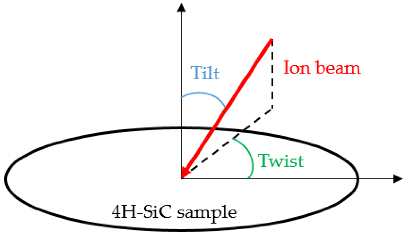
2.1. Ion Implantation of the Samples

For this study, successive ion implantations of the samples were performed in order to form a homogeneous doped film and enable the formation of dopant-related point defects and defect complexes within the silicon carbide layer. The implantations were performed using three different ion beam facilities in France [18,19,20]. The dopants were nitrogen (N) and aluminum (Al). The energy and dose of implantation varied from 20 to 400 eV and from 6.81 × 10¹¹ to 1.5 × 1015 cm−2, respectively. Most of the samples were implanted at room temperature (RT), with some of them at 300 and 400 °C. All details are provided in Table 1.
The samples originated from the same silicon carbide wafer commercialized by WolfSpeed (formerly named CREE) [21]. It was an 8°1′ off-axis n-type 4H-SiC wafer on which a 10 µm thick epilayer was grown with a nitrogen doping of 8.80 × 1015 cm−3. Before ion implantation, the samples were immersed in hydrofluoric acid (HF) to remove any silicon dioxide (SiO2) potentially present on their surface. For each sample, the tilt and twist angles of implantation were, respectively, 7 and 90° (Figure 1). Sample A23 was not implanted and was kept as a reference.

2.2. Dopant Concentration Estimation

I2SiC simulation software was used to determine the concentration profiles of the dopants and generated silicon vacancies within the silicon carbide samples. This software is based on the Monte Carlo (MC) method and, more particularly, on the binary collision approximation (BCA) [22]. This simulator took into account the crystalline structure of the silicon carbide sample, the temperature of implantation, and the deviation of the trajectory of the ions due to the defects generated by former implantations [23]. A comparison of the simulated results with secondary ion mass spectrometry (SIMS) measurements was also realized to validate the simulation model.

2.3. Cathodoluminescence Measurements

Cathodoluminescence measurements (CL) were realized using a SPARC (Delmic) system coupled to a JEOL JSM-7900F scanning electron microscope (SEM) to identify the color centers generated through the ion implantations. CL measurements were realized at 80K, with the samples being cooled down by support with liquid nitrogen circulation (80K Cryo-module, Kammrath & Weiss GmbH, Schwerte, Germany). A grating of 302 L/mm with a central wavelength at 500 nm was used, and a voltage of 15 kV with a current of 1 nA was applied. The spectral detection range of the CL setup extends up to 1200 nm.
Cathodoluminescence emission is produced due to the recombination of electron–hole pairs generated by the electron beam. Primary electrons can lose energy in a solid by exciting phonons and plasmons, as well as valence and inner shell electrons [24]. Each of these processes contributes to the generation of electron–hole pairs. Plasmons can decay into excitons [25], and the excitation of valence electrons produces electron–hole pairs. Moreover, photoelectrons, Auger electrons, and X-rays can excite valance electrons, and phonons assist in momentum conservation in indirect electronic transitions. It has been suggested that, to a first approximation, the local electron–hole pair generation rate within the electron interaction volume can be approximated using the local (average) total electron energy loss profile [26,27]. By integrating the total electron energy loss profile of the CL, the generation rate within the electron interaction volume in materials that exhibit negligible minority carrier diffusion can, therefore, be determined.
CL measurements were realized before and after annealing the samples at 900 °C for 15 min to observe the recombination of defects, which occurs at higher temperatures, and its effect on light emission. The annealing of the samples was realized under argon (Ar) in a chamber of an AET furnace equipped with graphite resistors and susceptors (Figure 2). The geometry of this heating chamber was designed to achieve a high temperature (up to 1900 °C) and rapid (2 °C/s) temperature process (RTP) on SiC samples with a width of up to 150 mm.

3. Results

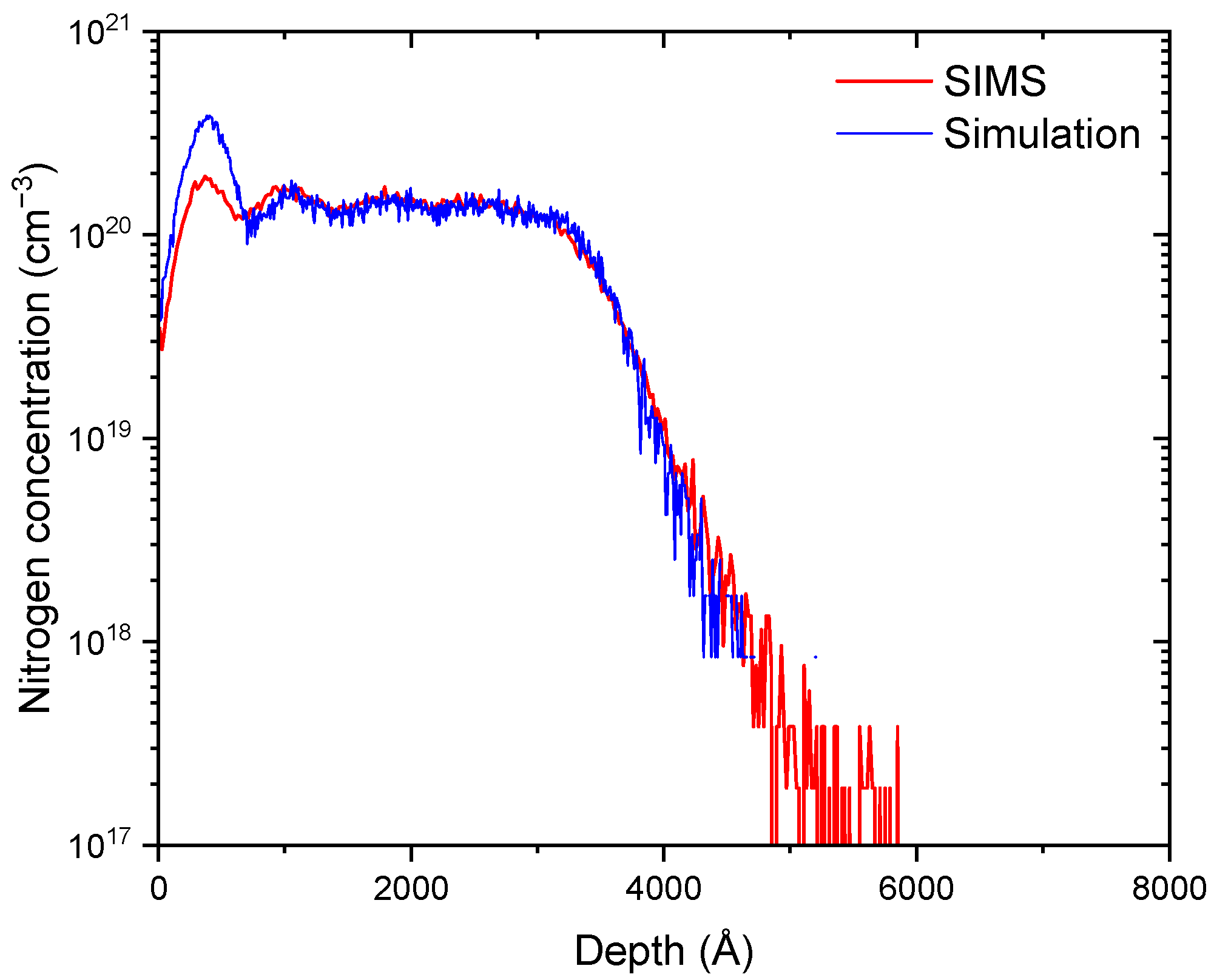
3.1. Dopant and Silicon Vacancy Concentration Profiles

The simulated and measured nitrogen concentrations of sample A17 are shown in Figure 3. The profile of concentration obtained using the I2SiC software follows the one obtained by SIMS quite well, even for the last channeling part. The main difference is the peak of nitrogen concentration observed at 375 Å, which is more elevated in the simulation compared to the SIMS measurements.
The simulated dopant and silicon vacancy concentration profiles of all the samples are shown in Figure 4. Due to the successive ion implantations, the simulated profiles of the dopants form a plateau at maximal concentration. The depth of the silicon vacancies within the n-doped 4H-SiC epilayer is similar to the one of the dopants Al and N. Compared to the ion-implanted concentrations, the concentration of VSi is higher and does not drop near the surface of the sample. It can be seen that a higher energy of implantation leads to a deeper implantation of the dopants and so a deeper generation of silicon vacancies. As expected, samples implanted with a more elevated dose present a higher concentration of dopants. The same tendency is also observed for the concentration of silicon vacancies, except for sample A9, which presents a higher VSi concentration than A12, whereas its total ion implantation dose is lower. A9 is also the only sample implanted with aluminum instead of nitrogen, which explains this phenomenon (aluminum is a heavier element).

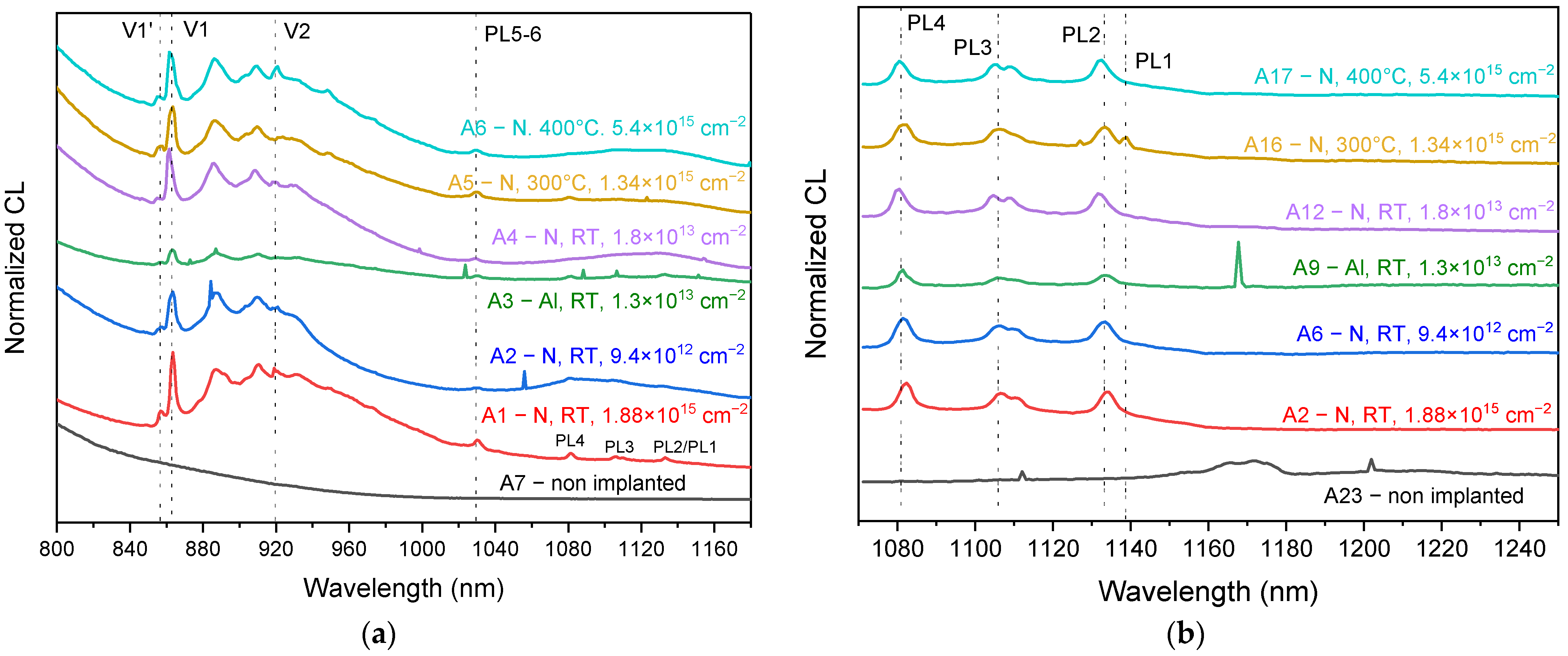
3.2. Cathodoluminescence Results

As shown in previous works [4,28,29,30], ion implantation of 4H-SiC leads to the generation of point defects, which, after annealing, can recombine or disappear. CL observations at 80K show that directly after ion implantation, all samples present a luminescence around 900 nm, which is typically related to the generation of silicon vacancies within 4H-SiC. The peaks observed at 856, 862, and 912 nm, named, respectively, V1′, V1, and V2 in Figure 5a, can be associated with the different configurations of the silicon vacancy in 4H-SiC [31]. The peak at 855 nm is notably more intense than the one at 862 nm, which indicates a preferential disposition of the silicon vacancies within the crystallographic lattice of 4H-SiC (Table 2).
The relative CL intensity of the V1′ peak is shown in Figure 5b for the different samples. It can be seen that samples A9 and A12 present a lower relative CL of the V1′ peak compared to the other samples. A9 corresponds to the only aluminum-implanted sample and A12 to room temperature, low-energy, and low-dosed nitrogen ion implantation (Table 1).
After annealing at 900 °C for 15 min, the luminescence around 900 nm is still visible. The V1′ and V1 peaks are still in the same position, but the V2 peak has red-shifted from 912 nm to 919 nm (Figure 6a). Moreover, this time, the V1 peak is more intense than the V1′ one. This indicates a change in the disposition of the silicon vacancies within the 4H-SiC crystal lattice. Other peaks also appear between 1020 and 1050 nm. The peaks PL1 to PL4 are situated at 1139, 1133, 1110, and 1080 nm. (Figure 6b). They can be associated with the different zero phonon lines (ZPLs) of the divacancy defect VSiVC (Table 2) [32]. The peak named PL5-6 at 1030 nm (Figure 6a) can be associated with the defects PL5 or PL6, whose ZPLs are at 1038 and 1040 nm, respectively (Table 2) [32].
Figure 7a shows the relative CL intensity of the peaks V1 and PL4 for the different samples. By tracing the relative CL intensity of the V1 peak in the function of the intensity of the PL4 peak, a linear behavior is found (Figure 7b). The intensities of these peaks are proportional to each other, and the relation between them can be expressed by the following formula:
y x = 2.78598 ± 0.07 x
with x representing the relative intensity of the PL4 peak and y the relative intensity of the V1 peak.
Sample A9, which is Al-implanted, presents the lowest CL intensity of the peaks V1 and PL4. In contrast, sample A2, which is N-implanted at RT with the highest dose (1.88 × 1015 cm−2) and at high energy (first implantation at 400 keV), presents the highest CL intensity. With regard to the relative intensity of the PL5-6 peak (Figure 7c), the intensity is still maximal for sample A2 but is minimal for samples A6, A9, and A12, which are all implanted at RT with low doses (around 1013 cm−2).

4. Discussion

The identification of the CL peaks was achieved by comparing the experimental results we obtained with values from the literature (Table 2). According to previous works, due to the particular crystallography of 4H-SiC, silicon vacancies can be localized on two different sites: one pseudo-cubic (k) and one hexagonal (h) [4]. Thus, the silicon vacancy in 4H-SiC is associated with two ZPLs emissions that are supposed to be at 862 and 917 nm, named, respectively, V1 and V2 (Table 2). The V1 site presents two different excited states for the same ground state, named 4A2 and 4E, which are known as the V1 and V1′ ZPLs, respectively. They can be selectively excited by lasers at 1.445 eV (858 nm) for 4E and 1.440 eV (862 nm) for 4A2. The intensity of the V1′ ZPL is also known to increase at elevated temperatures [10,33]. Recently, V1 was attributed to the hexagonal site (h) and V2 to the pseudo-periodic site (k) [31,34], in contrast to what was supposed previously [35].
Before annealing, the three peaks obtained through CL measurements at 856, 862, and 912 nm, respectively, correspond to the lines V1′, V1, and V2 (Figure 5). The intensity of the V1′ peak is greater than that of the V1 peak, no matter what the conditions of ion implantation are. Therefore, the silicon vacancies localized on the hexagonal site are mainly in the higher excited state V1′. This may be due to the energy loss in the sample epitaxial layer by the implanted ions, via inelastic and elastic collisions with the silicon and carbon atoms [36]. Therefore, the intensity of the V1′ peak shows that the generation of silicon vacancies is also dependent on the ion implantation conditions (Figure 5). The implantation of aluminum (sample A9) seems to generate fewer silicon vacancies in the V1′ state than nitrogen implantation. Indeed, in the SiC lattice, aluminum only substitutes for silicon, whereas nitrogen takes the place of carbon atoms only. Thus, the silicon vacancies generated through ion implantation can be partially replaced by aluminum atoms [37,38]. By comparing the samples A12, A6, and A2, all implanted at RT, the intensity of the V1′ peak is maximal for ion implantations with higher energy (A6 is more intense than A12). Between both ion implantations realized at RT under high energy (400 keV for the first implantation), the V1′ peak is more intense for the A6 sample, which was implanted with a lower dose (around 1013 cm−2) than the A2 sample (around 1015 cm−2). This can be related to the fact that high ion-implanted doses at RT tend to lead to the amorphization of the 4H-SiC layers close to the surface [39].
Moreover, when considering the samples A12, A16, and A17, which are implanted with nitrogen at almost the same energy range, the sample with the highest implanted dose presents the most intense V1′ peak. This may be due to the higher ion implantation temperatures of A16 and A17 (300 and 400 °C, respectively) which do not allow for amorphization close to the surface, preserving a sufficiently high silicon vacancy concentration. The V1′ peak is also known for its enhancement in intensity at high temperatures [33].
According to Figure 4, deeper nitrogen implantation of the dopants and, therefore, deeper generation of silicon vacancies occur for a higher energy of implantation, whereas the temperature of implantation does not seem to have an impact on this depth. Thus, a higher concentration of silicon vacancies in the hexagonal site of 4H-SiC, in the more excited state V1′, seems to be favored for ion implantations of nitrogen at a higher energy and temperature (with higher energies also generating deeper defects in the 4H-SiC layers).
After post-implantation annealing, the silicon vacancies can recombine into other point defects such as divacancies (VCVSi) and NV color centers [40]. Photoluminescence measurements realized with 325 nm laser excitation at RT showed that the 4H-SiC samples present a peak at 380 nm associated with the bandgap of 4H-SiC. A large band centered at 550 nm was also present, and is commonly associated with the N-Al donor–acceptor pair in 4H-SiC with the addition of boron into the material [41,42]. The cathodoluminescence results show that annealing for 15 min at 900 °C leads to an increase in the CL intensity of the V1 peak and the apparition of other peaks between 1020 and 1050 nm. According to the literature, these new peaks correspond to the ZPLs of the divacancy VCVSi within 4H-SiC [32]. Indeed, because the carbon and silicon vacancies can be placed on a cubic or hexagonal site of 4H-SiC, the divacancy has four different configurations, which are hh, kk, hk, and kh, corresponding to ZPLs named PL1 (1132 nm), PL2 (1131 nm), PL3 (1108 nm), and PL4 (1078 nm), respectively (Table 2) [2]. Three ZPLs named PL5, PL6, and PL7 have also been associated with the divacancy defect. Recently, Ivady et al. attributed them to divacancies trapped in quantum wells generated by stacking fault structure [32]. The PL5 and PL7 defects are basal plane-oriented, in contrast to the PL6 defect, which is c-axis-oriented. They are also attributed to the configurations k1h1 and k2k1 of 6H-SiC inclusions in 4H-SiC (Table 2) [32], and their symmetry was determined to be C1H [43]. However, very little work has been carried out to confirm the attribution of the PL5 to PL7 ZPLs to the presence of stacking faults in 4H-SiC. N.T. Son et al. observed the presence of these modified divacancies after annealing an electron-irradiated semi-insulating (HPSI) 4H-SiC substrate, but not in n- or p-doped substrates irradiated and annealed in the same conditions [43]. Therefore, the attribution of the PL5 to PL7 ZPLs to the presence of stacking faults in 4H-SiC is still a subject open to discussion. In Figure 6a, the peak at 1030 nm can be associated with the PL5 or PL6 defect.
Compared to the CL spectra of the samples directly after ion implantation, the V1 peak is now more intense than the V1′ one, after annealing at 900 °C. The relative intensity of this peak is also proportional to the relative intensity of the PL4 peak (Figure 7a,b). Thus, the annealing enables the displacement or generation of silicon vacancies in the hexagonal site of 4H-SiC in the state V1, which is more stable than V1′. Moreover, the increase in silicon vacancies in the V1 configuration leads to the generation of divacancies within the implanted samples. The proportionality between the V1 and PL4 peaks can be explained by the need for silicon vacancies to be in the V1 configuration to form divacancies. This time, the intensity of the V1 and PL4 peaks is still minimal for the aluminum-implanted sample (A9). Their CL intensities also seem to be related to the damage generated in the sample during ion implantation. In this case, annealing at 900 °C would have partially healed the damage and partial “amorphization” caused by ion implantation, which impedes the generation of silicon vacancies. Indeed, sample A2 presents the highest CL intensity for these peaks, and it is the sample supposed to be the most damaged during ion implantation due to the high dosage of nitrogen implanted at RT. Moreover, the samples A12, A16, and A17 have almost the same CL intensity for the V1 and PL4 peaks, which can be explained by the fact that low implanted doses of nitrogen (around 1013 cm−2) and high temperature of implantation (300–400 °C) limit the damage caused to the 4H-SiC samples. The CL intensity of the peaks for sample A6 is slightly lower, likely because it has the lowest implanted dose compared to the other samples. Thus, the generation of divacancies and V1 centers for silicon vacancies seems to depend on the used dopants (Al or N) and the damage caused during ion implantation.
Concerning the relative CL intensity of the PL5-6 peak (Figure 7c), it seems to be related to the temperature of implantation and the dose of implanted species independently of the nature of the dopant. Indeed, the PL5-6 peak is more intense for implantations at RT with high implanted doses (around 1015 cm−2). This intensity decreases when the temperature of implantation increases. Finally, the lowest peak intensities are for the samples implanted with low implanted doses (samples A12, A9, and A6). This tendency follows the association of the PL5-6 peak with stacking faults in 4H-SiC of Ivani et al. [32]. Indeed, a higher implanted dose during implantations is expected to increase the density of stacking faults in the lattice material. According to the literature, the presence of this peak means that the stacking faults are related to the presence of 6H-SiC polytypic inclusions in the 4H-SiC samples.

5. Conclusions

Ion implantations of the 4H-SiC samples led to the generation of silicon vacancies, which were characterized using cathodoluminescence. Directly after implantation, these vacancies were preferentially in the more excited V1′ configuration, which was favored by nitrogen ion implantation with high energy and/or high temperature.
After annealing at 900 °C for 15 min, it was found that the silicon vacancies were preferentially in the more stable V1 configuration, which led to the generation of divacancies within the 4H-SiC layers. The concentration of these defects seemed to be higher for nitrogen implantations, which damaged the samples more. A peak related to the PL5 or PL6 defects was also detected and related to the stacking faults produced during ion implantation. In this work, we focused only on the defect emission between 800 and 1300 nm. The cathodoluminescence of the defects below this emission range was not studied.
The processes presented, ion implantation and annealing, can be inserted into the fabrication of 4H-SiC nanophotonic devices including NIR-emitting silicon vacancies and divacancies. The annealing temperature is close to the temperature values for the classic step used during 4H-SiC device fabrication (annealing for ohmic contacts, thermal oxidation) and much lower compared to the temperatures needed to activate doping (~1700 °C) [39]. The recombination of silicon and carbon vacancies into divacancies generally occurs for annealing temperatures between 800 and 1100 °C after ion implantation. It is also at these temperatures that NV color centers are formed [28]. Higher-temperature annealing in this temperature range should be performed under argon in future works to determine the possible recombination of defects after ion implantation. These results will determine the compatibility and when the silicon vacancy and/or divacancy generation step should be inserted during the device process flow fabrication.

Author Contributions

Conceptualization, M.L. and E.V.; investigation, E.V., N.B., F.E. and M.L.; writing—original draft preparation, E.V.; writing—review and editing, M.L, N.B., F.E. and E.V.; supervision, M.L.; project administration, M.L. All authors have read and agreed to the published version of the manuscript.

Funding

This research received no external funding.

Acknowledgments

Samples were ion-implanted at the Pprime Institut (LMP), Poitiers, IJCLab (CSNSM), Orsay, and IP2I (IPNL), Lyon. SIMS measurements were realized at GEMAC in Versailles (France) by François Jomard. The authors also acknowledge the use of resources from the Nanomat platform (www.nanomat.eu, accessed on 2 January 2020), part of the Renatech platform, supported by the Ministère de l’Enseignement Supérieur et de la Recherche, the Région Grand Est, and FEDER funds from the European Community.

Conflicts of Interest

The authors declare no conflict of interest.

References

  1. She, X.; Huang, A.Q.; Lucía, Ó.; Ozpineci, B. Review of Silicon Carbide Power Devices and Their Applications. IEEE Trans. Ind. Electron. 2017, 64, 8193–8205. [Google Scholar] [CrossRef]
  2. Maximilians, J. Optical Spectroscopy on Silicon Vacancy Defects in Silicon Carbide. Ph.D. Thesis, Universität Würzburg, Würzburg, Germany, 2015. [Google Scholar]
  3. Al Atem, A.S. Ingénierie des Centres Colorés Dans SiC Pour la Photonique et la Solotronique; Université de Lyon: Lyon, France, 2019. [Google Scholar]
  4. Castelletto, S.; Boretti, A. Silicon Carbide Color Centers for Quantum Applications. J. Phys. Photonics 2020, 2, 022001. [Google Scholar] [CrossRef]
  5. Liu, J.; Xu, Z.; Song, Y.; Wang, H.; Dong, B.; Li, S.; Ren, J.; Li, Q.; Rommel, M.; Gu, X.; et al. Confocal Photoluminescence Characterization of Silicon-Vacancy Color Centers in 4H-SiC Fabricated by a Femtosecond Laser. Nanotechnol. Precis. Eng. 2020, 3, 218–228. [Google Scholar] [CrossRef]
  6. Matsunami, H. Fundamental Research on Semiconductor SiC and Its Applications to Power Electronics. Proc. Jpn. Acad. Ser. B Phys. Biol. Sci. 2020, 96, 235–254. [Google Scholar] [CrossRef]
  7. Norman, V.A.; Majety, S.; Wang, Z.; Casey, W.H.; Curro, N.; Radulaski, M. Novel Color Center Platforms Enabling Fundamental Scientific Discovery. InfoMat 2021, 3, 869–890. [Google Scholar] [CrossRef]
  8. Selnesaunet, G.M. Nanostructuring of SiC for Novel Defect-Based Quantum Technologies; University of Oslo: Oslo, Norway, 2021. [Google Scholar]
  9. Anderson, C.P.; Glen, E.O.; Zeledon, C.; Bourassa, A.; Jin, Y.; Zhu, Y.; Vorwerk, C.; Crook, A.L.; Abe, H.; Ul-Hassan, J.; et al. Five-Second Coherence of a Single Spin with Single-Shot Readout in Silicon Carbide. Sci. Adv. 2022, 8, eabm5912. [Google Scholar] [CrossRef]
  10. Majety, S.; Saha, P.; Norman, V.A.; Radulaski, M. Quantum Information Processing with Integrated Silicon Carbide Photonics. J. Appl. Phys. 2022, 131, 130901. [Google Scholar] [CrossRef]
  11. Castelletto, S.; Maksimovic, J.; Katkus, T.; Ohshima, T.; Johnson, B.C.; Juodkazis, S. Color Centers Enabled by Direct Femto-Second Laser Writing in Wide Bandgap Semiconductors. Nanomaterials 2021, 11, 72. [Google Scholar] [CrossRef]
  12. Eble, B. Nitrogen Vacancy Center in Cubic Silicon Carbide: A Promising Qubit in the 1.5μm Spectral Range for Photonic Quantum Networks. Phys. Rev. B 2018, 98, 165203. [Google Scholar] [CrossRef]
  13. Khanaliloo, B.; Jayakumar, H.; Hryciw, A.C.; Lake, D.P.; Kaviani, H.; Barclay, P.E. Single-Crystal Diamond Nanobeam Waveguide Optomechanics. Phys. Rev. X 2015, 5, 041051. [Google Scholar] [CrossRef]
  14. Song, Y.; Xu, Z.; Li, R.; Wang, H.; Fan, Y.; Rommel, M.; Liu, J.; Astakhov, G.; Hlawacek, G.; Li, B.; et al. Photoluminescence and Raman Spectroscopy Study on Color Centers of Helium Ion-Implanted 4H–SiC. Nanomanuf. Metrol. 2020, 3, 205–217. [Google Scholar] [CrossRef]
  15. Gao, S.; Duan, Y.-Z.; Tian, Z.-N.; Zhang, Y.-L.; Chen, Q.-D.; Gao, B.-R.; Sun, H.-B. Laser-Induced Color Centers in Crystals. Opt. Laser Technol. 2022, 146, 107527. [Google Scholar] [CrossRef]
  16. Hallén, A.; Linnarsson, M. Ion Implantation Technology for Silicon Carbide. Surf. Coat. Technol. 2016, 306, 190–193. [Google Scholar] [CrossRef]
  17. Ziegler, J.F.; Ziegler, M.D.; Biersack, J.P. SRIM—The Stopping and Range of Ions in Matter (2010). Nucl. Instrum. Methods Phys. Res. Sect. B Beam Interact. Mater. At. 2010, 268, 1818–1823. [Google Scholar] [CrossRef]
  18. Oliviero, E.; Lazar, M.; Gardon, A.; Peaucelle, C.; Perrat, A.; Grob, J.J.; Raynaud, C.; Planson, D. High Energy N+ Ion Implantation in 4H–SiC. Nucl. Instrum. Methods Phys. Res. Sect. B Beam Interact. Mater. At. 2007, 257, 265–269. [Google Scholar] [CrossRef]
  19. Burcea, R.; Barbot, J.-F.; Renault, P.-O.; Eyidi, D.; Girardeau, T.; Marteau, M.; Giovannelli, F.; Zenji, A.; Rampnoux, J.-M.; Dilhaire, S.; et al. Influence of Generated Defects by Ar Implantation on the Thermoelectric Properties of ScN. ACS Appl. Energy Mater. 2022, 5, 11025–11033. [Google Scholar] [CrossRef]
  20. Zheng, C.; Gentils, A.; Ribis, J.; Kaïtasov, O.; Borodin, V.A.; Descoins, M.; Mangelinck, D. The Feasibility of Al-Based Oxide Precipitation in Fe–10%Cr Alloy by Ion Implantation. Philos. Mag. 2014, 94, 2937–2955. [Google Scholar] [CrossRef]
  21. Silicon Carbide Power & GaN RF Solutions|Wolfspeed. Available online: https://www.wolfspeed.com/ (accessed on 27 April 2023).
  22. Morvan, E. Modélisation de l’implantation Ionique Dans α-SiC et Application à La Conception de Composants de Puissance. Ph.D. Thesis, Institut National des Sciences Appliquées de Lyon, Lyon, France, 1999. [Google Scholar]
  23. Morvan, E.; Mestres, N.; Campos, F.J.; Pascual, J.; Hallén, A.; Linnarsson, M.K.; Kuznetsov, A.Y. Damage Reduction in Channeled Ion Implanted 6H-SiC. Mater. Sci. Forum 2000, 338–342, 893–896. [Google Scholar] [CrossRef]
  24. Shimizu, R.; Ze-Jun, D. Monte Carlo Modelling of Electron-Solid Interactions. Rep. Prog. Phys. 1992, 55, 487. [Google Scholar] [CrossRef]
  25. Yunogami, T.; Mizutani, T. Radiation Damage in SiO2/Si Induced by Low-energy Electrons via Plasmon Excitation. J. Appl. Phys. 1993, 73, 8184–8188. [Google Scholar] [CrossRef]
  26. Everhart, T.E.; Hoff, P.H. Determination of Kilovolt Electron Energy Dissipation vs Penetration Distance in Solid Materials. J. Appl. Phys. 2003, 42, 5837–5846. [Google Scholar] [CrossRef]
  27. Werner, U.; Koch, F.; Oelgart, G. Kilovolt Electron Energy Loss Distribution in Si. J. Phys. Appl. Phys. 1988, 21, 116–124. [Google Scholar] [CrossRef]
  28. Wang, J.-F.; Yan, F.-F.; Li, Q.; Liu, Z.-H.; Liu, H.; Guo, G.-P.; Guo, L.-P.; Zhou, X.; Cui, J.-M.; Wang, J.; et al. Coherent Control of Nitrogen-Vacancy Center Spins in Silicon Carbide at Room Temperature. Phys. Rev. Lett. 2020, 124, 223601. [Google Scholar] [CrossRef] [PubMed]
  29. Bracher, D.O.; Hu, E.L. Fabrication of High- Q Nanobeam Photonic Crystals in Epitaxially Grown 4H-SiC. Nano Lett. 2015, 15, 6202–6207. [Google Scholar] [CrossRef] [PubMed]
  30. Koehl, W.F.; Buckley, B.B.; Heremans, F.J.; Calusine, G.; Awschalom, D.D. Room Temperature Coherent Control of Defect Spin Qubits in Silicon Carbide. Nature 2011, 479, 84–87. [Google Scholar] [CrossRef]
  31. Ivády, V.; Davidsson, J.; Son, N.T.; Ohshima, T.; Abrikosov, I.A.; Gali, A. Identification of Si-Vacancy Related Room-Temperature Qubits in $4H$ Silicon Carbide. Phys. Rev. B 2017, 96, 161114. [Google Scholar] [CrossRef]
  32. Ivády, V.; Davidsson, J.; Delegan, N.; Falk, A.L.; Klimov, P.V.; Whiteley, S.J.; Hruszkewycz, S.O.; Holt, M.V.; Heremans, F.J.; Son, N.T.; et al. Stabilization of Point-Defect Spin Qubits by Quantum Wells. Nat. Commun. 2019, 10, 5607. [Google Scholar] [CrossRef]
  33. Bracher, D.O.; Zhang, X.; Hu, E.L. Selective Purcell Enhancement of Two Closely Linked Zero-Phonon Transitions of a Silicon Carbide Color Center. Proc. Natl. Acad. Sci. USA 2017, 114, 4060–4065. [Google Scholar] [CrossRef]
  34. Nagy, R.; Niethammer, M.; Widmann, M.; Chen, Y.-C.; Udvarhelyi, P.; Bonato, C.; Hassan, J.U.; Karhu, R.; Ivanov, I.G.; Son, N.T.; et al. High-Fidelity Spin and Optical Control of Single Silicon-Vacancy Centres in Silicon Carbide. Nat. Commun. 2019, 10, 1954. [Google Scholar] [CrossRef]
  35. Wagner, M.; Magnusson, B.; Chen, W.M.; Janzén, E.; Sörman, E.; Hallin, C.; Lindström, J.L. Electronic Structure of the Neutral Silicon Vacancy in 4H and 6H SiC. Phys. Rev. B 2000, 62, 16555–16560. [Google Scholar] [CrossRef]
  36. Favennec, P.-N. l’Implantation Ionique. Pour la Microélectronique et l’Optique; Masson, E., Ed.; CNET-ENST: Paris, France, 1993. [Google Scholar]
  37. Mattausch, A.; Bockstedte, M.; Pankratov, O. Ab-Initio Study of Dopant Interstitials in 4H-SiC. Mater. Sci. Forum 2005, 483–485, 523–526. [Google Scholar] [CrossRef]
  38. Pernot, J.; Contreras, S.; Camassel, J. Electrical Transport Properties of Aluminum-Implanted 4H–SiC. J. Appl. Phys. 2005, 98, 023706. [Google Scholar] [CrossRef]
  39. Lazar, M.; Raynaud, C.; Planson, D.; Chante, J.-P.; Locatelli, M.-L.; Ottaviani, L.; Godignon, P. Effect of Ion Implantation Parameters on Al Dopant Redistribution in SiC after Annealing: Defect Recovery and Electrical Properties of p-Type Layers. J. Appl. Phys. 2003, 94, 2992–2998. [Google Scholar] [CrossRef]
  40. Zargaleh, S.A.; Eble, B.; Hameau, S.; Cantin, J.-L.; Legrand, L.; Bernard, M.; Margaillan, F.; Lauret, J.-S.; Roch, J.-F.; von Bardeleben, H.J.; et al. Evidence for Near-Infrared Photoluminescence of Nitrogen Vacancy Centers in 4H-SiC. Phys. Rev. B 2016, 94, 060102. [Google Scholar] [CrossRef]
  41. Kakanakova-Georgieva, A.; Yakimova, R.; Henry, A.; Linnarsson, M.K.; Syväjärvi, M.; Janzén, E. Cathodoluminescence Identification of Donor–Acceptor Related Emissions in as-Grown 4H–SiC Layers. J. Appl. Phys. 2002, 91, 2890–2895. [Google Scholar] [CrossRef]
  42. Ottaviani, L.; Hidalgo, P.; Idrissi, H.; Lancin, M.; Martinuzzi, S.; Pichaud, B. Structural Characterization of 6H- and 4H-SiC Polytypes by Means of Cathodoluminescence and X-ray Topography. J. Phys. Condens. Matter 2003, 16, S107. [Google Scholar] [CrossRef]
  43. Son, N.T.; Shafizadeh, D.; Ohshima, T.; Ivanov, I.G. Modified Divacancies in 4H-SiC. J. Appl. Phys. 2022, 132, 025703. [Google Scholar] [CrossRef]
Figure 1. Illustration of the ion implantation angles.
Coatings 13 00992 g001
Figure 2. AET RTP graphite resistive furnace picture (a); usual temperature and pressure profiles (b).
Coatings 13 00992 g002
Figure 3. SIMS and simulated nitrogen concentration profiles of sample A17. Implantation was realized at 400 °C with a total dose of 5.4 × 1015 cm−2 and maximal energy of 190 eV.
Coatings 13 00992 g003
Figure 4. Simulated concentration profiles of the dopants (a) and silicon vacancies (b) for samples A2 to A17. All samples are implanted with nitrogen except for A9, which is implanted with aluminum.
Coatings 13 00992 g004
Figure 5. Normalized CL measurements of implanted 4H-SiC samples (a) and relative intensity of the V1’ peak (b). Peaks are indexed by vertical dashed lines.
Coatings 13 00992 g005
Figure 6. Normalized CL measurements of ion-implanted 4H-SiC samples after 900 °C annealing for 15 min, centered at 950 nm (a) and 1300 nm (b).
Coatings 13 00992 g006
Figure 7. Relative CL intensity of V1, PL4 (a), and PL5-6 (c) peaks after 900 °C annealing for 15 min. (b) Relative CL intensity of V1 in the function of PL4.
Coatings 13 00992 g007
Table 1. Ion implantation parameters of the 4H-SiC samples.
NameDopantTemperature [°C]Energy [keV]Dose [cm−2]
A2N15RT4006.4 × 1014
2704.6 × 1014
1704 × 1014
1003.8 × 1014
Total: 1.88 × 10¹⁵
A6NRT4003.2 × 1012
2702.3 × 1012
1702 × 1012
1001.9 × 1012
Total: 9.4 × 10¹²
A9AlRT3005.93 × 1012
1902.9 × 1012
1152.08 × 1012
601.42 × 10¹²
256.81 × 10¹¹
Total: 1.3 × 10¹³
A12NRT1905.6 × 1012
1353.6 × 1012
903.4 × 10¹²
503.2 × 10¹²
302.2 × 10¹²
Total: 1.8 × 10¹³
A16N3001605 × 1014
1102.8 × 1014
702.5 × 10¹⁴
401.8 × 10¹⁴
201.3 × 10¹⁴
Total: 1.34 × 10¹⁵
A17N4001901.5 × 1015
1359 × 1014
909 × 1014
508 × 1014
201.3 × 10¹⁵
Total: 5.4 × 10¹⁵
A23NANANANA
Table 2. Observed defects characteristics.
DefectsConfigurationDesignationZPLs (nm)
Theory [3,4,31,32]
ZPLs (nm)
Experimental
VSihV1, V1′862, 858862, 856
kV2917912–919
VCVSihhPL111321139
kkPL211311133
khPL311081110
hkPL410781080
VCVSi near a stacking fault (ssf)k1h1-ssfPL510421030
k2k2-ssfPL61038
k2k1-ssfPL7unknown
Disclaimer/Publisher’s Note: The statements, opinions and data contained in all publications are solely those of the individual author(s) and contributor(s) and not of MDPI and/or the editor(s). MDPI and/or the editor(s) disclaim responsibility for any injury to people or property resulting from any ideas, methods, instructions or products referred to in the content.

