Article

Electronic and Electrical Properties of Island-Type Hybrid Structures Based on Bi-Layer Graphene and Chiral Nanotubes: Predictive Analysis by Quantum Simulation Methods

by
Michael M. Slepchenkov
1,
Pavel V. Barkov
1 and
Olga E. Glukhova
1,2,*
1
Institute of Physics, Saratov State University, Astrakhanskaya Street 83, 410012 Saratov, Russia
2
Laboratory of Biomedical Nanotechnology, I.M. Sechenov First Moscow State Medical University, Trubetskaya Street 8-2, 119991 Moscow, Russia
*
Author to whom correspondence should be addressed.
Coatings 2023, 13(5), 966; https://doi.org/10.3390/coatings13050966
Submission received: 1 February 2023 / Revised: 6 May 2023 / Accepted: 15 May 2023 / Published: 22 May 2023

Abstract

:
Hybrid structures based on graphene and carbon nanotubes (CNTs) are one of the most relevant modern nanomaterials for applications in various fields, including electronics. The variety of topological architectures of graphene/CNT hybrids requires a preliminary study of their physical properties by in silico methods. This paper is devoted to the study of the electronic and electrical properties of graphene/CNT hybrid 2D structures with an island topology using the self-consistent charge density functional-based tight-binding (SCC-DFTB) formalism and the Landauer–Buttiker formalism. The island-type topology is understood as the atomic configuration of a graphene/CNT hybrid film, in which the structural fragments of graphene and nanotubes form “islands” (regions of the atomic structure) with an increased density of carbon atoms. The island-type graphene/CNT hybrid structures are formed by AB-stacked bilayer graphene and (6,3)/(12,8) chiral single-walled carbon nanotubes (SWCNT). The bilayer graphene is located above the nanotube perpendicular to its axis. Based on the binding energy calculations, it is found that the atomistic models of the studied graphene/SWCNT hybrid structures are thermodynamically stable. The peculiarities of the band structure of graphene/SWCNT (6,3) and graphene/SWCNT (12,8) hybrid structures are analyzed. It is shown that the electronic properties of graphene/SWCNT hybrid structures are sensitive to the orientation and size of the graphene layers with respect to the nanotube surface. It is found that an energy gap of ~0.1 eV opens in the band structure of only the graphene/SWCNT (6,3) hybrid structure, in which the graphene layers of the same length are arranged horizontally above the nanotube surface. We revealed the electrical conductivity anisotropy for all considered atomistic models of the graphene/SWCNT (12,8) hybrid structure when bilayer graphene sheets with different sizes along the zigzag and armchair directions are located at an angle with respect to the nanotube surface. The obtained knowledge is important to evaluate the prospects for the potential application of the considered atomic configurations of graphene/SWCNT hybrid structures with island-type topology as connecting conductors and electrodes in electronic devices.

1. Introduction

For several decades, graphene and carbon nanotubes have been the most discussed representatives of the carbon allotropes family [1,2,3,4,5]. Combining graphene and CNTs into a hybrid structure marked the transition to a new direction in materials science [6,7,8,9,10,11,12,13,14,15]. Graphene/CNT hybrid nanostructures have a larger surface area, porosity, thermal conductivity, mechanical strength, and improved optical, electrical, and electrochemical properties compared to their structural components [16,17,18,19]. Another advantage of graphene/CNT hybrid structures is improved hydrophobic characteristics. This makes them a promising material in environmental applications [20]. The excellent physical and chemical properties of graphene/CNT hybrid nanostructures open up wide opportunities for their application as flexible and transparent electrodes in field-effect transistors, energy storage devices, field emitters, sensors, and hydrogen storage systems [21,22,23,24,25,26].
Various approaches have been developed for the synthesis of graphene/CNT hybrid structures. They are usually divided into two groups, namely assembly methods and in situ methods [12]. Assembly methods use technologies such as vacuum filtration, sol-gel synthesis, layer-by-layer assembly, electrophoretic deposition, and solution processing [6]. Using the assembly methods, graphene/CNT hybrid structures with non-covalent interaction between CNTs and graphene are experimentally obtained. To obtain graphene/CNT hybrids with a covalent seamless junction of nanotubes and graphene, in situ, methods are used, including chemical vapor deposition, chemical unzipping, etc. [6]. The possibilities of modern synthesis technologies make it possible to obtain graphene/CNT hybrid structures with various architectures. Depending on the orientation of graphene and CNTs, all graphene/CNT hybrid structures are divided into three types [12]: (1) hybrids, where CNTs are horizontally oriented with respect to graphene; (2) hybrids, where CNTs are vertically oriented with respect to graphene; (3) hybrids, where CNTs are wrapped with graphene. The most common type of graphene/CNT hybrids is the first type listed above [12].
Computer simulation methods are actively used to conduct research aimed at revealing new physical effects and phenomena in graphene/CNT hybrid structures of various topologies. Quite a few papers are devoted to the theoretical study of the electronic and heat-conducting properties of seamless graphene/CNT heterostructures with vertically oriented CNTs [27,28,29,30,31,32,33,34,35]. Using the tight binding method, Matsumoto and Saito found that the graphene/SWCNT (6,6) hybrid structures have a band gap of 0.27 eV (in the case of SWCNTs with open ends) and 0.51 eV (in the case of SWCNTs with closed ends) [30]. A similar effect of opening a band gap of 0.2 eV was observed for a 3D carbon network formed by (5,5) SWCNTs embedded in graphene on both sides of the sheet [31]. Novaes et al. studied the transport properties of graphene/SWCNT hybrid structures with vertically oriented (4,4) and (8,0) SWCNTs using ab initio methods [32]. In some papers [33,34,35], the thermal conductivity of graphene/SWCNT hybrid structures with vertically oriented (6,6) SWCNTs was calculated. It has been shown that the heat flux in seamless 3D graphene/SWCNT (6,6) hybrid structures are determined by the minimum distance between the nanotubes and their length [34]. Interesting calculation results have been obtained for graphene/SWCNT hybrid structures with horizontally oriented SWCNTs [36,37,38,39,40,41,42]. The mechanical and electronic properties of graphene/SWCNT (12,0) and graphene/SWCNT (8,0) hybrids have been studied [36,37,38]. In these hybrid structures, nanotubes are covalently bonded to one or more graphene nanoribbons with a width equal to the SWCNT length. It has been established that the graphene/SWCNT (12,0) and graphene/SWCNT (8,0) hybrid structures are characterized by Van Hove singularities and a higher Young’s modulus compared to individual nanotubes and graphene. In addition, the graphene/SWCNT (8,0) hybrid structure is characterized by the presence of an energy gap between the valence and conduction bands of several hundreds of a meV. Of great interest to researchers is quantum transport in graphene/SWCNT hybrid structures with horizontally oriented SWCNTs. The influence of such factors as the conductivity of SWCNTs [39], the graphene-SWCNT distance [40], and graphene nanoribbon’s width and shape [41] on the quantum electron transport in graphene/SWCNT hybrid structures has been analyzed. The regularities of interaction of graphene/SWCNT hybrid 2D structures with covalently bonded graphene and horizontally oriented (10,0) and (12,0) SWCNTs with electromagnetic radiation in infrared, visible, and ultraviolet ranges have been studied [42]. It was shown that high-intensity optical conductivity peaks appear in the UV and optical ranges, regardless of the nanotube diameter and distance between them.
In the past few years, the attention of researchers has been turned to the development of technologies for obtaining graphene/SWCNT hybrid 2D structures with improved strength properties. In particular, Advincula et al. demonstrated the synthesis of a 2D graphene/SWCNT network by flash Joule heating of initial carbon nanotubes without the use of solvents and gases [43]. It was shown that a hybrid 2D network of covalently bonded SWCNTs and graphene is promising as an effective reinforcing additive in epoxy composites. The hardness and Young’s modulus of graphene/SWCNT hybrid-based epoxy composites increase by 162% and 64%, respectively, compared with the neat epoxy. Li et al. have proposed an economical and scalable approach to obtain thin hybrid films based on SWCNTs and graphene nanoplatelets prepared by the spray-coating method [44]. In the hybrid structure, SWCNTs interacted with graphene nanoplates by means of van der Waals forces. In this case, the nanoplates overlapped each other and onto the nanotubes, forming networks with “islands” of increased carbon density. A strain sensor based on a hybrid graphene/SWCNT network is characterized by high sensitivity (calibration factor ~197 at 10% strain) and extensibility (≥50%), as well as a reproducible response over 1000 load cycles. In addition, new prototypes of nanoelectronic devices based on graphene/SWCNT hybrid structures continue to be developed. Shin et al. have fabricated a p-type barrister based on a hybrid 2D structure formed by van der Waals joined graphene and a semiconductor SWCNT with a diameter of 1.3 nm [45]. The fabricated barrister showed an electron mobility of ~5350 cm2/Vs and current on/off ratio of 106. Using palladium-catalyzed partial unzipping of SWCNTs, intramolecular heterojunctions based on graphene nanoribbons (2.4 nm in width) and SWCNTs (0.8 nm in diameter) were obtained [46]. The photovoltaic device based on these heterojunctions demonstrated a large open-circuit voltage of 0.52 V and a high efficiency of external power conversion of 4.7% under illumination with a wavelength of 1550 nm. Computational studies of recent years are mainly aimed at revealing the features of the atomic structure of various topological configurations of graphene/SWCNT hybrids and calculating their energy and electrical parameters. McDaniel conducted a fixed-voltage molecular dynamics study of the influence of structural features on the capacitance of electrodes based on a graphene/SWCNT hybrid [47]. The electrodes consist of different numbers of (9,9) or (12,12) SWCNTs stacked on a graphene sheet. It was found that the points of contact between graphene and SWCNTs serve as “hot spots” with significantly improved charge separation compared to the rest of the electrode. Xu and Jiang performed an MD study of the atomic configuration of a van der Waals heterostructure graphene/SWCNT/graphene using a mechanical model based on the competition between the bending energy and the adhesion energy [48]. According to the results of numerical simulations, it was found that the cross-section of the nanotube is compressed into an ellipse by graphene layers, and the eccentricity of the ellipse increases with increasing nanotube diameter. Wei and Zhang studied the formation mechanism of seamless junctions between vertically oriented SWCNTs (8,0) and a graphene monolayer with various topological defects [49] using the SCC-DFTB theory. Additionally, the authors calculated the Mülliken charge distribution for the construction of (8,0)-graphene SWCNT junctions. At the same time, in the above-mentioned papers with simulation results, graphene/SWCNT hybrid structures with nonchiral nanotubes are studied, while most of the synthesized SWCNTs are chiral nanotubes of sub-nanometer diameter [50].
The aim of this paper is to establish the effect of atomic structure features on the electronic properties and electrical conductivity of graphene/SWCNT hybrid structures with island-type topology formed by chiral nanotubes with a diameter of 0.6–1.3 nm and AB-stacked bilayer graphene. An island-type topology is understood as an atomic configuration of a graphene/SWCNT hybrid film in which the structural fragments of graphene and nanotubes form “islands” (regions of the atomic structure) with an increased density of carbon atoms). The features of the atomic structure will be understood as the mutual arrangement of graphene sheets in the bilayer graphene structure, the location of the bilayer graphene relative to the surface of the nanotube, the nanotube diameter, and the size of the graphene layer along the zigzag direction.

2. Calculation Details

The atomic structure and energy parameters of graphene/SWCNT hybrid structures with island topology were calculated using the SCC-DFTB method [51] implemented in the DFTB+ software package version 20.2 [52]. The tight binding approximation is included in the DFT model using perturbation theory [53]. This approximation is used at the stage of calculating the total energy of the system. The effect of electron density fluctuations on the total energy of the system is taken into account within the SCC-DFTB method. The distribution of the electron charge density over atoms is determined according to the Mulliken population analysis [54]. The valence approximation is used in the SCC-DFTB model. In accordance with the valence approximation, the largest contribution to the total energy of the system is made by the valence orbitals. In the course of SCC-DFTB calculations, the Slater-type orbitals with the set of pbc-0-3 parameters were used [52]. We chose the SCC-DFTB method due to the polyatomic nature of the supercells of graphene/SWCNT hybrid structures under study.
The electrical conductivity G was calculated within the framework of the Landauer–Buttiker formalism [55] according to the formula
G = I V = 2 e 2 h T E F T E E F d E ,
where T(E) is the transmission function of electrons, FT is the function of the thermal broadening of energy levels, EF is the Fermi level of the electrodes, e is the elementary charge, h is Planck’s constant, 2e2/h is the doubled value of the conductance quantum to account for the spin. The T(E) function is calculated using the equation [56]:
T E = 1 N k = 1 N Tr Γ S E G C A E Γ D E G C R E ,
where G C R E ,   G C A E   are the retarded and advanced Green’s functions describing the contact with electrodes, Γ S E , Γ D E   are the level broadening matrices for the left (source) and drain (right) electrodes, respectively. Figure 1 shows the scheme for the calculation of quantum electron transport using one of the atomistic models of the graphene/SWCNT (6,3) hybrid 2D structure. The left and right electrodes and the conducting channel (scattering region) are supercells of the graphene/SWCNT hybrid structure. We considered the current transfer in the directions of the X (Figure 1a) and Y (Figure 1b) axes. In the case of the current transfer along the X axis, the electrodes are semi-infinite in the direction of X axis and infinite in the direction of Y axis. In the case of the current transfer along the Y axis, the electrodes are semi-infinite in the direction of Y axis and infinite in the direction of the X axis.
An original method was used to speed up the calculation of T(E) of polyatomic supercells of graphene/SWCNT hybrids under study [57]. Within this method, the function T(E) was calculated for a small number of k-points of the first Brillouin zone. Then it was interpolated for any k-point of the first Brillouin zone and reconstructed the full function T(E). The temperature of 300 K was used in all calculations.

3. Results and Discussion

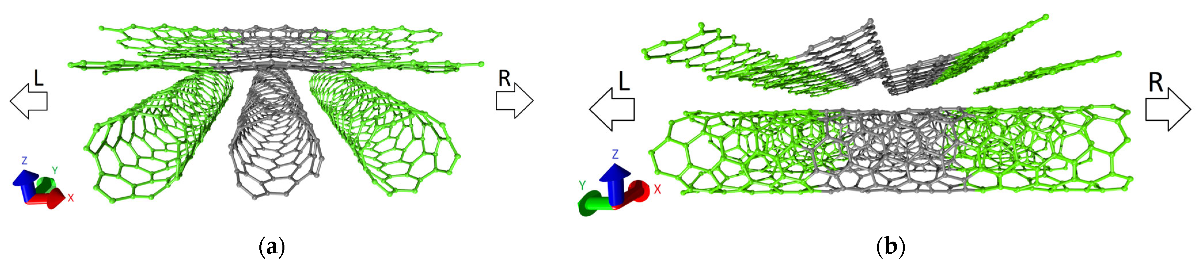
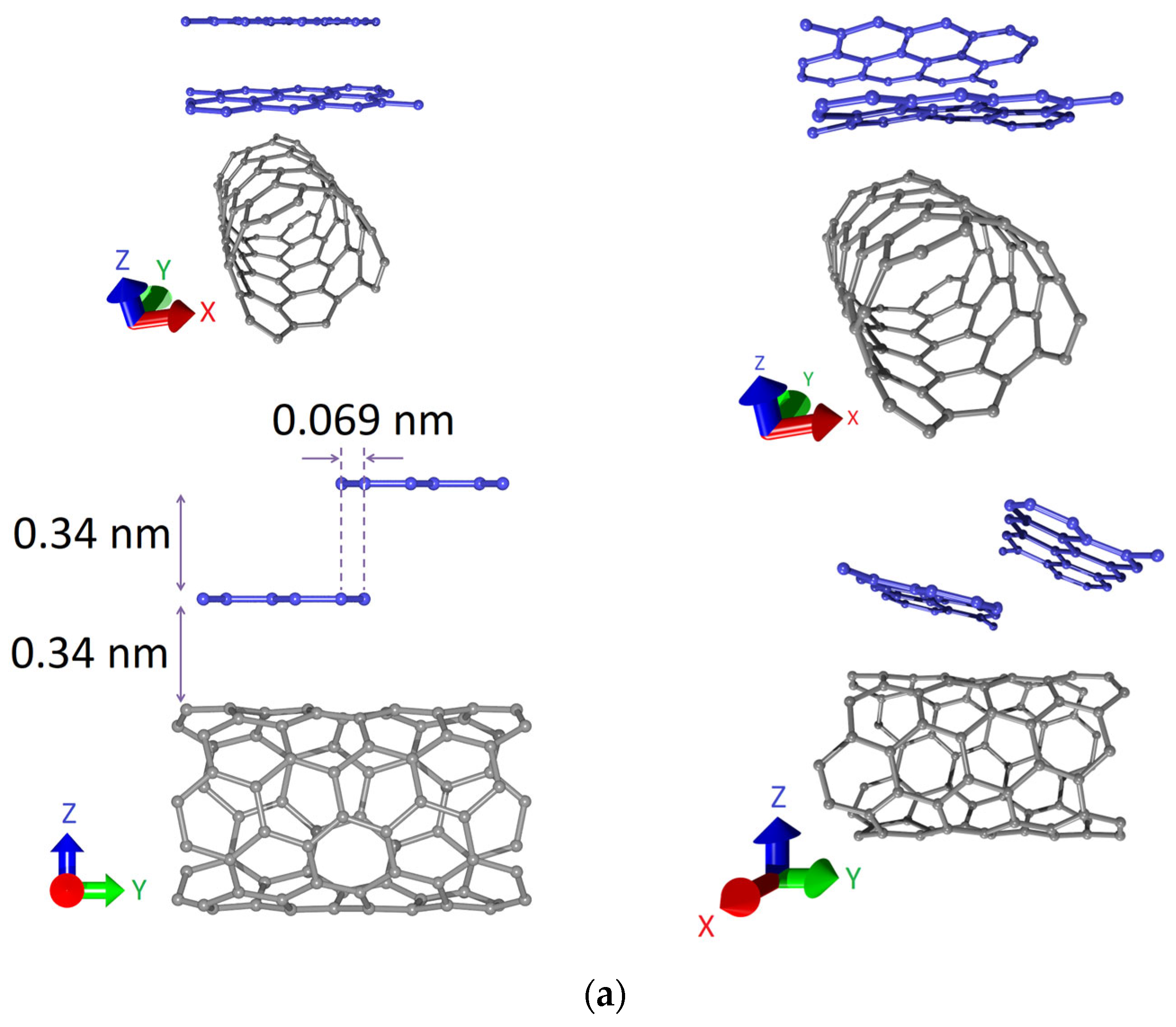
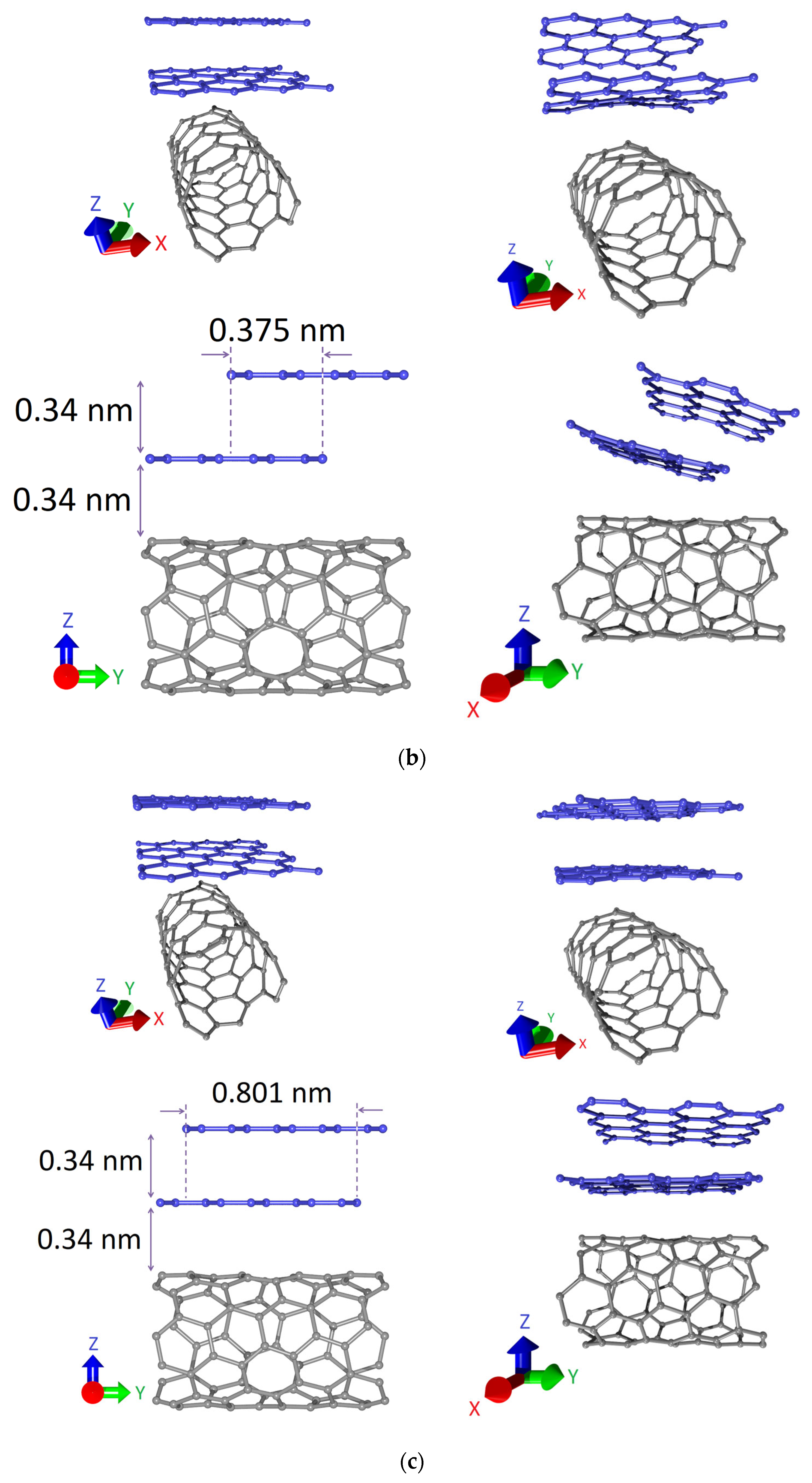
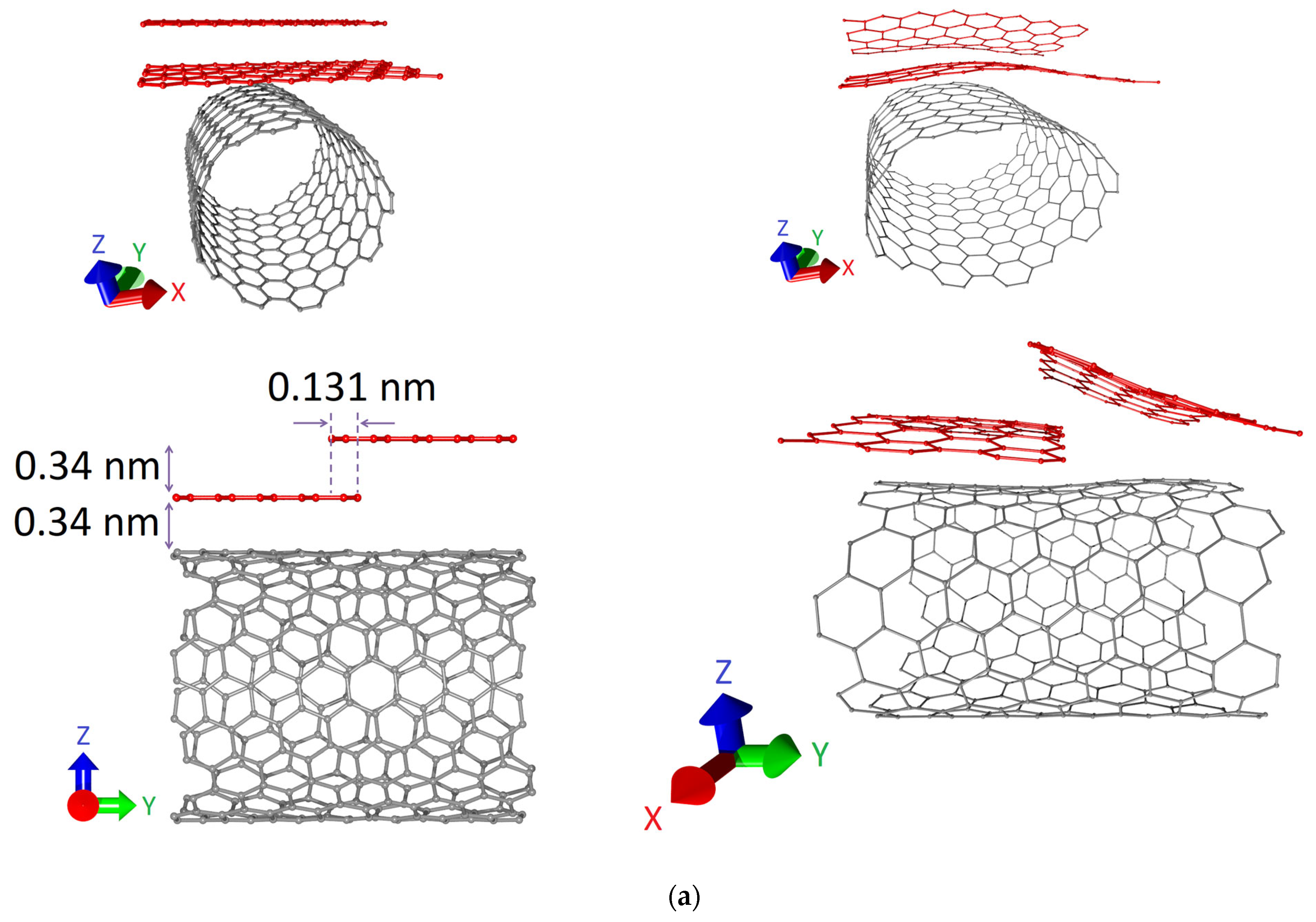
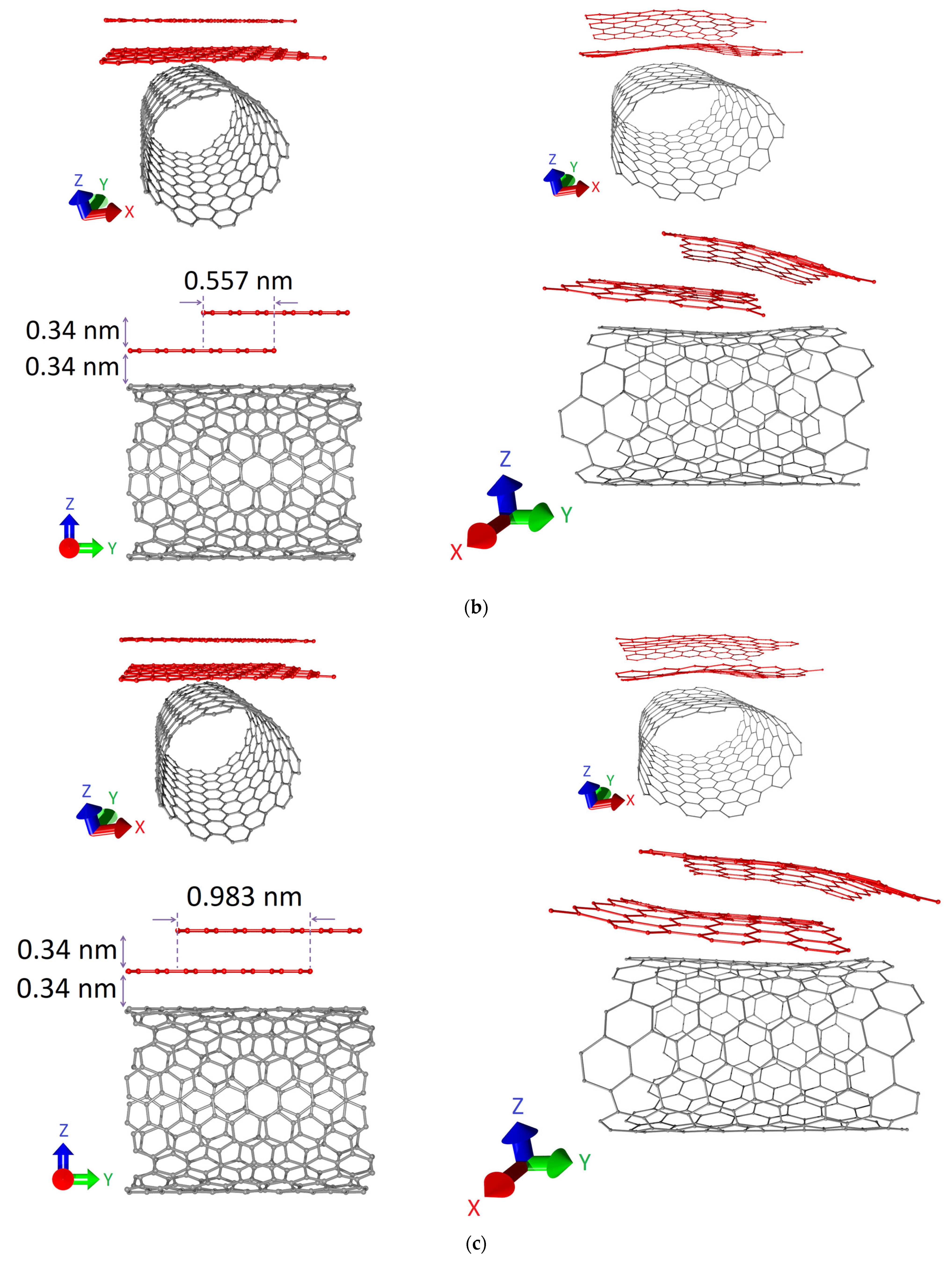
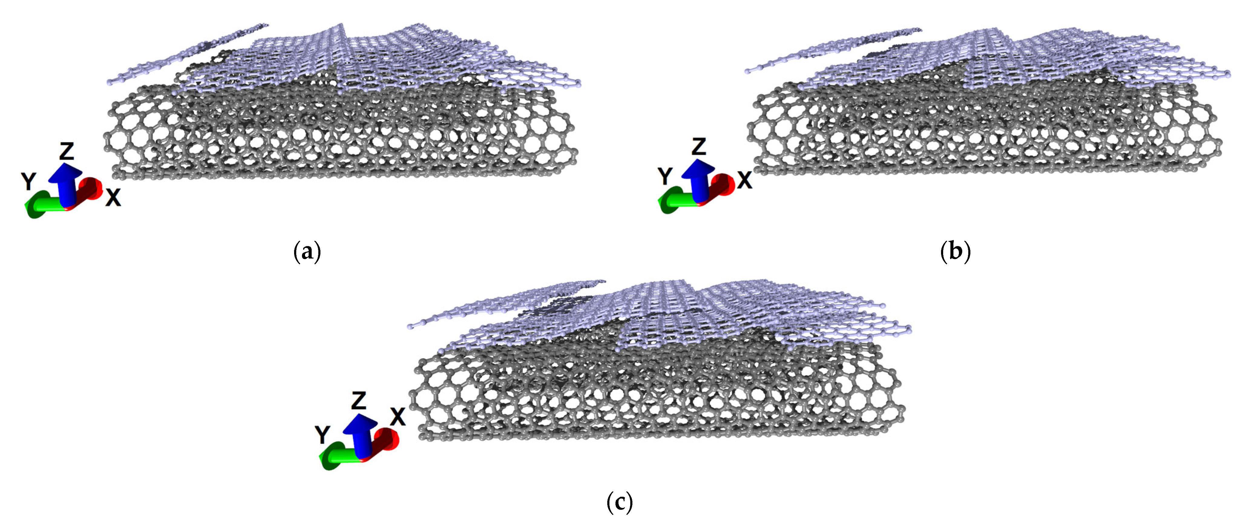
3.1. Atomistic Models of Graphene/SWCNT Hybrid Structures with Island-Type Topology

Two types of configurations of graphene/SWCNT hybrid 2D structures with island-type topology are considered in this paper: (1) configurations based on (6,3) SWCNTs with a diameter of ~0.63 nm with a metallic type of conductivity; (2) configurations based on (12,8) SWCNTs with a diameter of ~1.3 nm with a semiconductor type of conductivity. For each topological configuration, three atomistic models of a supercell were constructed. The supercell contains fragment of AB-stacked bilayer graphene which is located above the nanotube surface, forming the so-called “islands” of increased density of carbon atoms. The structures with such topology are obtained during the synthesis of graphene/CNT hybrids with horizontally oriented nanotubes [44]. The atomistic models differed in the size of the graphene fragment along the Y axis (in the armchair direction of the graphene sheet) and in the value of the shift of one graphene layer relative to another along the Y axis. For (6,3) SWCNTs, atomistic models were constructed with a size of graphene fragment along the Y axis of 2 hexagons (model V1), three hexagons (model V2), and four hexagons (model V3). The shift of one layer of graphene relative to another along the Y axis was 0.069 nm for model V1, 0.375 nm for model V2, and 0.801 nm for model V3. Bilayer graphene and nanotube were located at a distance of ~0.3 nm for all three models. The layers in bilayer graphene were located at a distance of ~0.3 nm in the direction of the Z axis. The translation vectors of the supercells of models V1, V2 and V3 were Lx = 0.984 nm and Ly = 1.127 nm after optimization of the atomic structure. Supercells of models V1, V2, and V3 of graphene/SWCNT (6,3) hybrid 2D structures before and after optimization of the atomic structure are shown in Figure 2.
As can be seen, in the cases of models V1 and V2, the sheets of bilayer graphene were deformed as a result of optimization of the atomic structure. They are located at a certain angle with respect to the nanotube surface. For model V3, the degree of deformation of bilayer graphene was minimal. The graphene sheets were arranged horizontally with respect to the nanotube surface. Differences in the orientation of graphene sheets with respect to the nanotube surface between the models are explained by the small size of graphene sheets in the armchair direction (along the Y axis) in the case of models V1 and V2. The nanotube (6,3) was almost not deformed due to its small size.
For (12,8) SWCNTs, atomistic models were constructed with a size of graphene fragment along the Y axis of 4 hexagons (model V1), five hexagons (models V2), and six hexagons (model V3). Since the length of SWCNT (1.857 nm) in the supercell of the graphene/SWCNT (12,8) hybrid structure is noticeably larger than in the supercell of the graphene/SWCNT (6,3) hybrid structure (1.127 nm), the size of the graphene fragment along the Y axis for topological configurations with (12,8) SWCNTs was chosen larger. The shift of one layer of graphene relative to another along the Y axis was 0.131 nm for model V1, 0.557 nm for model V2, and 0.983 nm for model V3. The distance between the graphene layers along the Z axis, as well as the distance between the graphene bilayer and nanotube, was chosen to be ~0.3 nm for all three models. The translation vectors of the supercells of models V1, V2 and V3 after optimization of the atomic structure were the same and amounted to Lx = 1.857 nm and Ly = 1.968 nm. Supercells of models V1, V2, and V3 of the graphene/SWCNT (12,8) hybrid 2D structures before and after optimization of the atomic structure are shown in Figure 3. It is clearly seen that, for all three models, a noticeable deformation of graphene sheets and nanotubes in the supercell is observed. The nanotube acquires the shape of an ellipsoid, shrinking along the Z axis.
The constructed supercells were tested for thermodynamic stability at room temperature. To do this, we calculated the binding energy Eb according to Equation (3):
E b = E h E g r E t u b e / N ,
where Eh is the energy of a graphene/SWCNT hybrid structure, Egr is the energy of a bilayer graphene, Etube is the energy of a nanotube, and N is the number of atoms in a supercell. The calculated values of Eb are given in Table 1. According to Table 1, each of the considered configurations is characterized by a negative binding energy. Therefore, the resulting atomic configurations of the supercells are energetically favorable.
Table 1 shows that model V3 has the highest thermodynamic stability among the considered supercells of the graphene/SWCNT (6,3) hybrid structures. This is due to the low degree of deformation of graphene sheets and the absence of deformation for the nanotube. The degree of deformation of the nanotube and graphene sheets in the supercells of the graphene/SWCNT (12,8) hybrid structures are approximately the same for all models. Therefore, the binding energies of these models are close in magnitude.

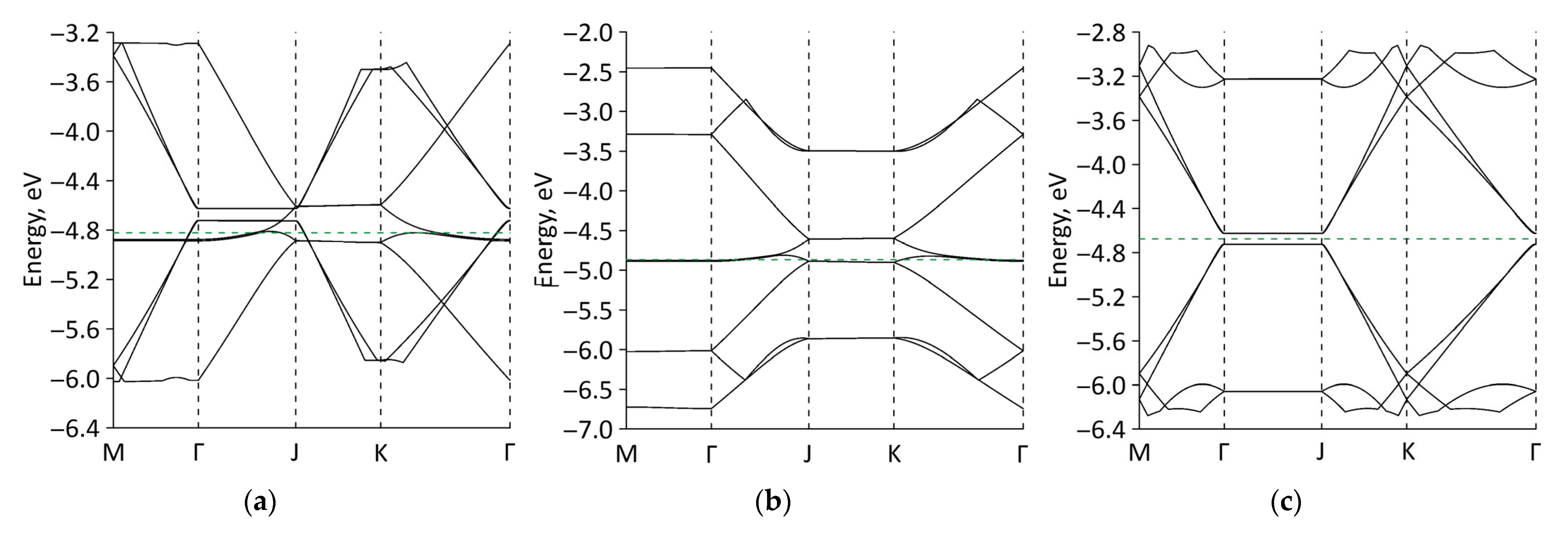
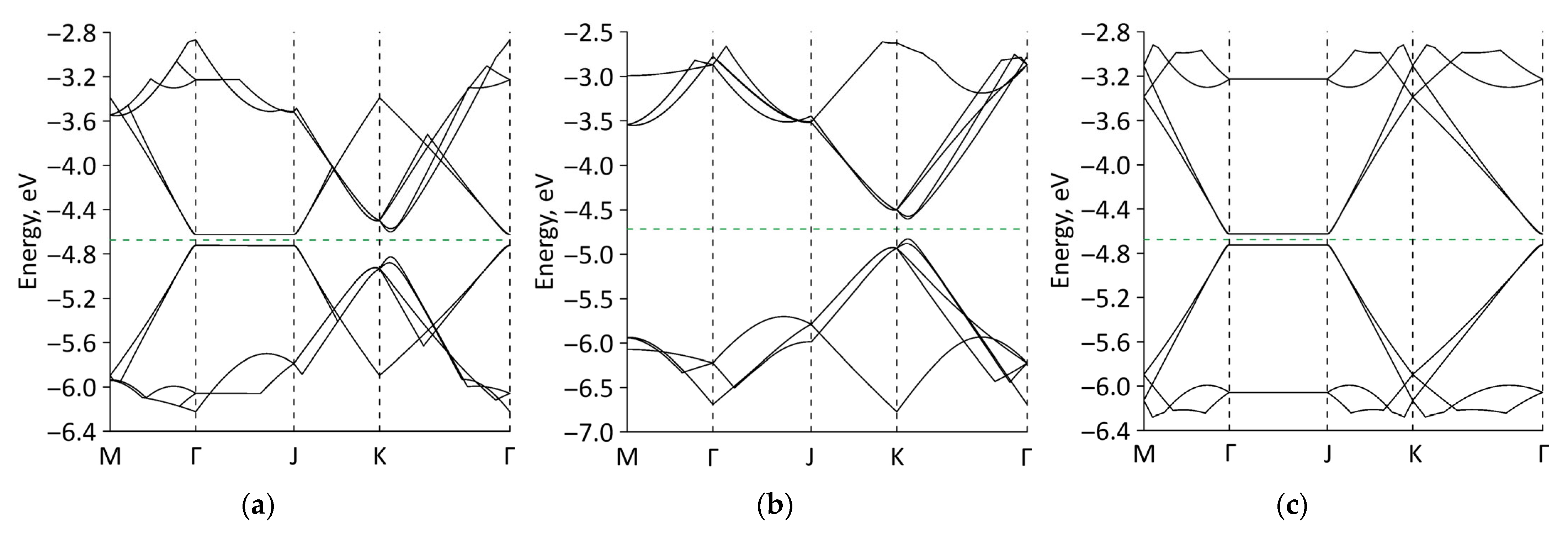
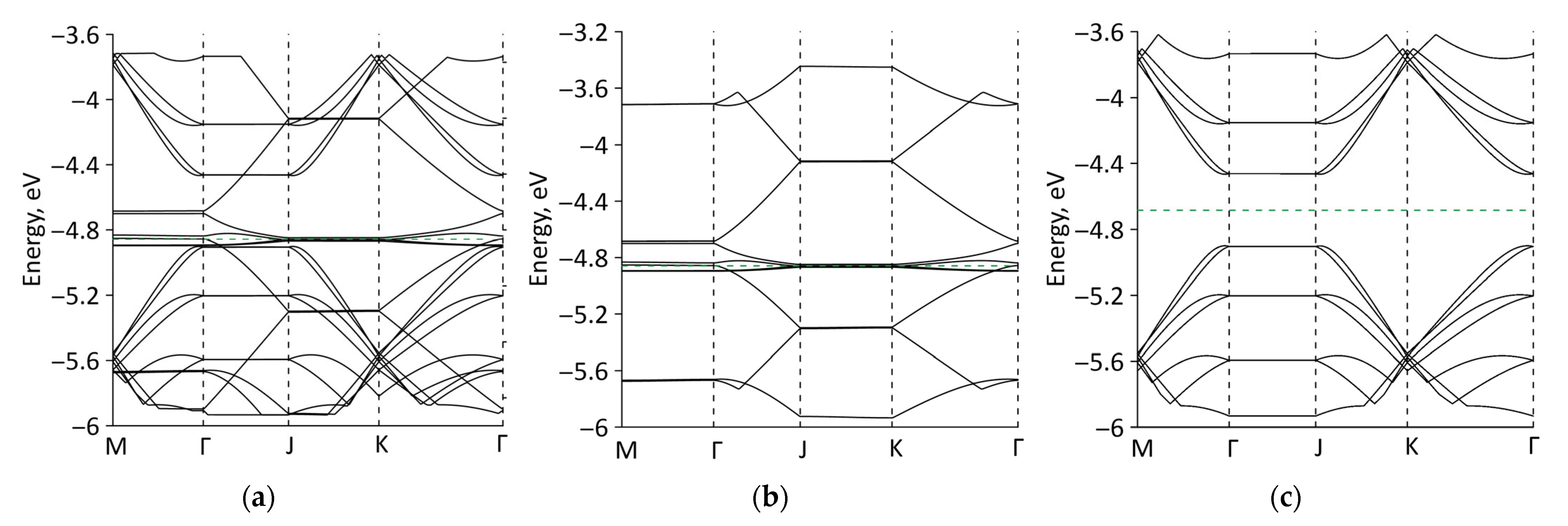
3.2. Electronic Properties of Graphene/SWCNT Hybrid Structures of Island Type

To understand the prospects for using the graphene/SWCNT (6,3) and graphene/SWCNT (12,8) hybrid films in nanoelectronic devices, it is necessary (1) to know the features of the electronic structure, including the patterns of formation of the band structure; (2) to understand the pattern of quantum electron transport, including for controlling the electrical conductivity. The key point of the study is to establish the possibility of topological control of the electronic–energetic and electrophysical parameters of graphene/SWCNT hybrid films. We consider the influence of such topological features as the mutual arrangement of graphene sheets in the bilayer graphene structure, the orientation of the bilayer graphene with respect to the nanotube surface, the nanotube diameter, and the size of the graphene layer along the zigzag direction.
To reveal the electronic structure features of graphene/SWCNT hybrid films with island-type topology, the energy band diagrams were calculated. The band structure was sampled along a path M–Γ–J–K–Γ within the first Brillouin zone. One of our tasks was to analyze what features of the electronic structure and properties of bilayer graphene and (6,3) and (12,8) SWCNTs are manifested in the graphene/SWCNT hybrid structures. Figure 4, Figure 5 and Figure 6 show the calculated band diagrams near the Fermi level for supercells of graphene/SWCNT (6,3) hybrid structures. These figures also show the band diagrams of a nanotube (6,3) and bilayer graphene, which are part of the supercell of the graphene/SWCNT (6,3) hybrid structure. Based on the results of the analysis of the presented diagrams, the following patterns can be identified. The band diagrams of graphene/SWCNT (6,3) hybrid structures of all three models contain characteristic features of the electronic structure of both bilayer graphene and (6,3) SWCNTs. The contribution of bilayer graphene to the energy profile near the valence band maximum (VBM) and near the conduction band minimum (CBM) is clearly seen between the highly symmetrical J and K points of the Brillouin zone. The contribution of (6,3) SWCNTs to the energy profile near the VBM and CBM manifests itself between Γ and J points. Between M and Γ, as well as between K and Γ points, the joint influence of bilayer graphene and (6,3) SWCNTs on the patterns of the energy profile of the graphene/SWCNT (6,3) hybrid structure.
An analysis of the band diagrams makes it possible to trace how the type of conductivity of the graphene/SWCNT (6,3) hybrid structure changes depending on the topological features of the supercells of models V1, V2, and V3. For supercells of models V1 and V2, no energy gap is observed between the VBM and CBM, which indicates the gapless nature of the band structure of these atomic configurations of graphene/SWCNT hybrids (6,3). A similar picture is also characteristic of the band structure of bilayer graphene, which is part of the supercells of these models. Model V3 is characterized by the appearance of an energy gap of ~0.1 eV between the VBM and CBM, which allows us to speak about the opening of an energy gap in the band structure. To explain this physical phenomenon, we considered how the position of the Fermi level changes in the energy band diagrams of the graphene/SWCNT (6,3) hybrid structure and its components (bilayer graphene and (6,3) SWCNTs). The values of the Fermi level are presented in Table 2. It can be seen that that in the case of models V1 and V2, the Fermi level (−4.82 eV) of the graphene/SWCNT (6,3) hybrid structure almost completely repeats the position of the Fermi level of the bilayer graphene fragment in the supercells of these topological models (−4.87 eV for the model V1and −4.86 eV for the model V2). As is known, it is the position of the Fermi level that determines both the type of conductivity and the basic electrophysical properties of the material. Taking into account the gapless band structure of a fragment of bilayer graphene from supercells of models V1 and V2 (see Figure 4 and Figure 5), we can say that for these models, it is bilayer graphene that makes a decisive contribution to the electronic properties and type of conductivity of the graphene/SWCNT (6,3) hybrid structure. In the case of model V3, the Fermi level (−4.67 eV) of the graphene/SWCNT (6,3) hybrid structure completely coincides with the Fermi level of the SWCNT (6,3) from the supercell of model V3. The size of the opened energy gap in the band structure of the graphene/SWCNT (6,3) hybrid is the same as that of the SWCNT (6,3). In addition, the energy gap in the band structure of the graphene/SWCNT (6,3) hybrid opens between the highly symmetrical points Γ and J of the Brillouin zone, just as in SWCNT (6,3). At the same time, in the case of model V3, an energy gap also opens in the band structure of a bilayer graphene fragment from the graphene/SWCNT (6,3) supercell. The Fermi level (−4.71 eV) of the bilayer graphene fragment from the model V3 supercell changes significantly compared to the Fermi level of the bilayer graphene fragment from the V1 and V2 models (−4.82 eV) and approaches the Fermi level of the hybrid structure (−4.67 eV). All this allows us to assume that in the case of model V3, both bilayer graphene and (6,3) SWCNTs affect the appearance of an energy gap in the band structure of the graphene/SWCNT (6,3) hybrid, but the contribution of (6,3) SWCNTs is decisive.
The reason for such noticeable differences between the model V3 and the models V1 and V2 is the different topology of bilayer graphene in these models. Let us illustrate them visually by the example of extended fragments of each of the models obtained by multiple translations of their supercells in two directions (along the X and Y axis). These fragments are shown in Figure 7. It can be seen that, for models V1 and V2, graphene layers of small width in the direction of the Y axis line up one after another at an angle with respect to the nanotube surface. In this case, the edge atoms of one graphene layer are located above the edge atoms of the other graphene layer, causing the curvature of their atomic network. In the extended fragment of model V3, the graphene layers are oriented horizontally with respect to the nanotube surface and have similar sizes in both directions of the supercell translation. Due to the arrangement of graphene layers of the same size in a horizontal plane, their atomic network has a minimum curvature, and the interaction at the level of electron orbitals is much weaker as a result. In addition, Figure 7c shows that the upper graphene layer in model V3 slightly rotated relative to the lower one, forming a twisted graphene structure. As was previously found, twisted bilayer graphene demonstrates the effect of opening the energy gap between the valence band and the conduction band [58].
The analysis of the electronic structure for the topological models of the graphene/SWCNT (12,8) hybrid structure was carried out in a similar manner. Let us trace the pattern of the energy subband profile of the graphene/SWCNT (12,8) hybrid structure using the model V1 as an example. Figure 8 shows the energy band diagrams of model V1 of the graphene/SWCNT (12,8) hybrid structure and its individual structural components. It can be seen that the graphene/SWCNT (12,8) hybrid has a gapless band structure, which is characteristic of bilayer graphene in the composition of the model V1 supercell. A completely identical picture of the energy subband profile of the band diagram is also observed for models V2 and V3. Since the degree of deformation of graphene layers and nanotube (12,8) is the same in the supercells of models V1, V2 and V3, no visible changes in the band structure of graphene/SWCNT (12,8) hybrid and its individual components are observed. Therefore, we confine ourselves to presenting the energy band diagrams for model V1.
The absence of differences in the band diagrams of the models V1, V2, and V3 of the graphene/SWCNT (12,8) hybrid structure can be explained by their similar topological features. This is clearly confirmed by the extended fragments of each of the models shown in Figure 9. In each of the cases, the graphene layers in the extended fragment are located at some angle with respect to the nanotube surface, like “steps of a ladder”. A similar pattern was observed earlier for models V1 and V2 of the graphene/SWCNT (6,3) hybrid structure.
The leading role of bilayer graphene in determining the type of conductivity of the graphene/SWCNT (12,8) hybrid structure is confirmed by the complete coincidence of the location of the Fermi level in their band structures: −4.858 eV for the model V1, −4.849 eV for the model V2, and −4.840 for the model V3.

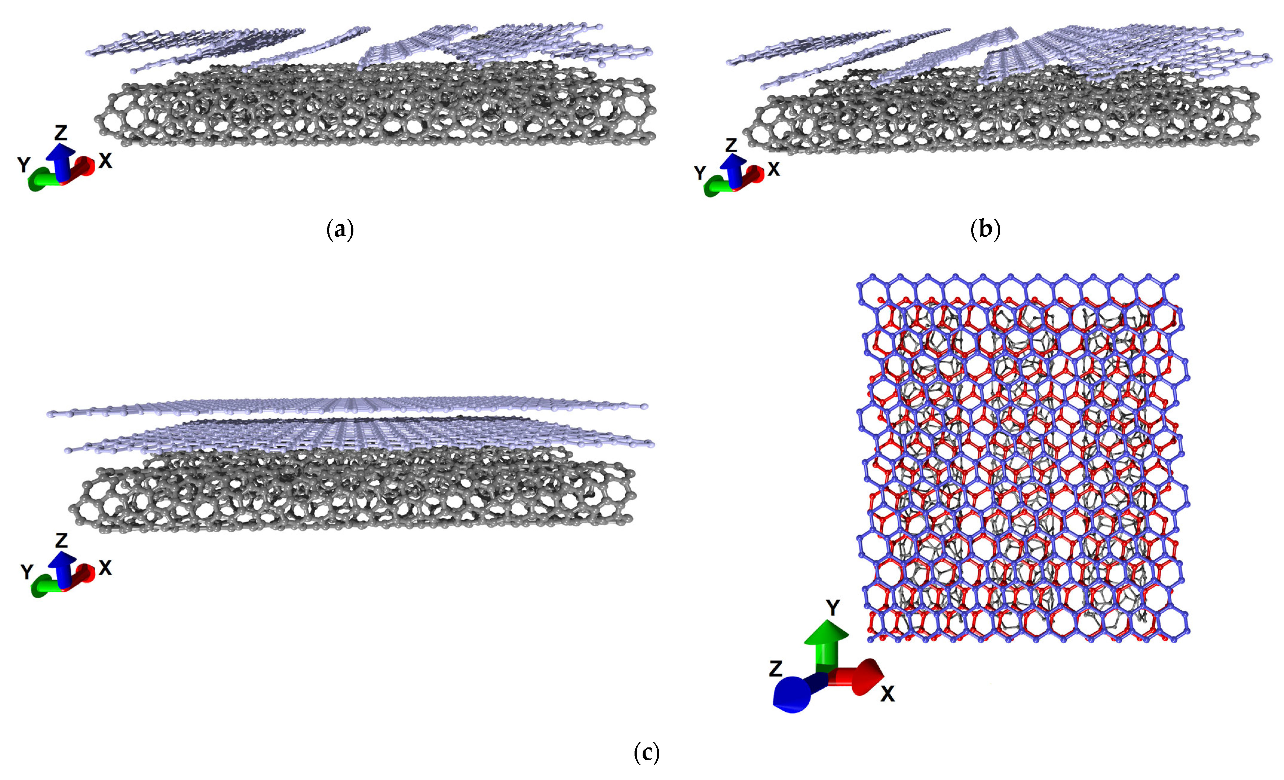
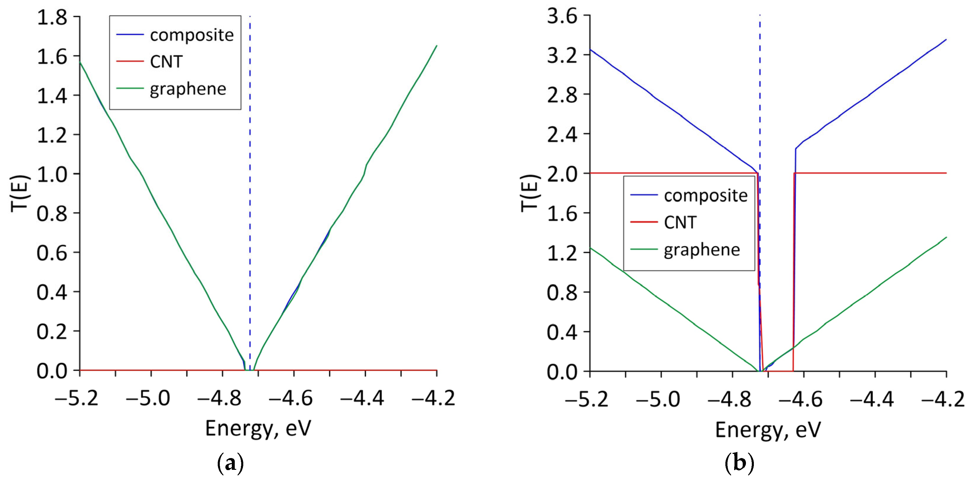
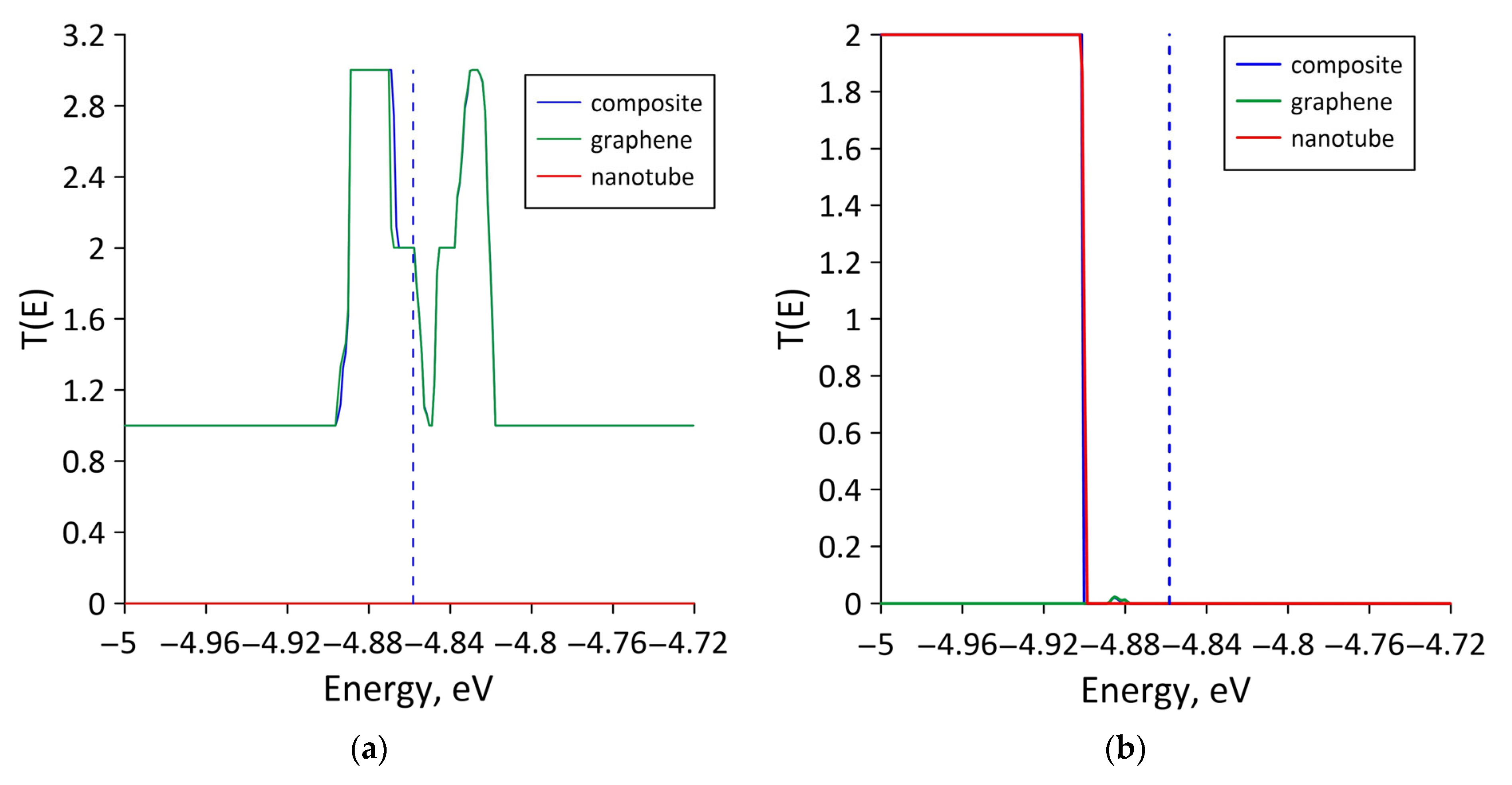
3.3. Electrical Properties of Graphene/SWCNT Hybrid Structures with Island-Type Topology

Having revealed the features of the electronic structure of the graphene/SWCNT (6,3) and graphene/SWCNT (12,8) hybrid structures with the island-type topology, we proceed to a discussion of their electrical properties. We evaluated the electrical properties by the magnitude of the electrical resistance, which is the main parameter of the connecting conductors in the circuits of various electronic devices. Table 3 shows the electrical resistances RX and RY calculated for models V1, V2 and V3 of the graphene/SWCNT (6,3) and graphene/SWCNT (12,8) hybrid structures in two directions of current transfer: along the zigzag direction (X axis) and along the armchair direction (Y axis) of graphene hexagonal lattice. The electrical resistance was defined as the reciprocal of the electrical conductivity G calculated according to Equation (2).
Table 3 shows that the resistance values of models V1 and V2 of the graphene/SWCNT (6,3) hybrid structure are almost the same in both directions of current transfer. The similarity in the resistance values of the models V1 and V2 is explained by the similarity of their topological features discussed above. In the case of model V3, the difference in the resistance values between the current transfer directions is almost 10 times. This indicates the presence of electrical conductivity anisotropy. In order to explain the observed anisotropy, Figure 10 shows graphs of the transmission function T(E) for model V3 (graphene/SWCNT (6,3) hybrid structure and its individual components) in two directions of current transfer (along the X and Y axes). It can be seen from the figure that the electrical conductivity anisotropy is due to the different number of conduction channels in the directions of current transfer: the values of T(E) near the Fermi level at current transport along the X axis are several times larger than for current transport along the Y axis. Consequently, in the case of current transport along the X axis, the graphene/SWCNT (6,3) hybrid takes on the properties of bilayer graphene; in the case of current transport along the Y axis, the graphene/SWCNT (6,3) hybrid takes the properties of SWCNT (6,3).
In the case of the graphene/SWCNT (12,8) hybrid structure, the electrical conductivity anisotropy is observed for all three atomistic models. Let us explain the observed anisotropy using model V1 as an example, analyzing the calculated T(E) profiles for the graphene/SWCNT (12,8) hybrid structure and its individual structural components. These profiles are shown in Figure 11. As in the case of the model V3 of the graphene/SWCNT (6,3) hybrid structure, the appearance of anisotropy is associated with a different number of conduction channels in two directions of current transfer: in the direction of the X axis, the values of T(E) near the Fermi level are several times larger than in the direction of Y axis. With an increase in the size of bilayer graphene along the Y axis (in the direction of the armchair of the graphene hexagonal lattice), the overlap area of the graphene layers increases, and, hence, the intensity of the electronic interaction between them and the nanotube in the region of “islands” of increased density of carbon atoms. This can explain the increase in the resistance RY during the transition from model V1 to model V3.
The electrical conductivity anisotropy revealed for model V3 of the graphene/SWCNT (6,3) hybrid structure and models V1, V2, and V3 of the graphene/SWCNT (12,8) hybrid structure is related to the topological and electronic structure features of bilayer graphene in the supercells of these models. Based on the data in Table 3, it can be concluded that the models V1 and V2 of the graphene/SWCNT (6,3) hybrid structure has the lowest electrical resistance values (~6–7 kOhm) in both directions of current transport. In terms of electrical resistance values, these atomic configurations of graphene/SWCNT hybrid structures are not inferior to the structures of pillared graphene (~10–30 kOhm) [57], hybrid films based on oxidized graphene and MWCNTs (~20 kOhm) [58], some varieties of carbon nanotube-reinforced polymer composites (~10–20 kOhm) [59] and graphene-based fiber-reinforced composite (~200 kOhm) [60].

4. Conclusions

In this article, for the first time, the issues of topological control of the electronic and electrical properties of graphene-nanotube hybrid films with island-type topology (fragments of graphene and nanotubes form “islands” with an increased density of carbon atoms) were considered in detail by changing various topological and geometric parameters of the hybrid film: nanotube diameter, size of the graphene fragment along the zigzag direction (along the Y axis), the shift of one layer of graphene relative to another along the zigzag direction (along the Y axis), orientation (tilt angle) of the bilayer graphene with respect to the nanotube surface. To build atomistic models of graphene/SWCNT hybrid 2D structures, we chose chiral (6,3) and (12,8) SWCNTs of sub- and nanometer diameters, which are most often encountered in the experiment. Based on the results of energy band diagram calculations, it was established that the electronic properties of graphene/SWCNT hybrid structures, in particular, the type of conductivity, are sensitive to the orientation and size of the graphene layers with respect to the nanotube surface. It has been found that an energy gap of ~0.1 eV opens in the band structure of the graphene/SWCNT (6,3) hybrid when graphene layers of the same length are arranged horizontally above the nanotube surface. When bilayer graphene sheets with different sizes along the zigzag and armchair directions are located at an angle with respect to the nanotube surface, for the graphene/SWCNT (12,8) hybrid structure, electrical conductivity anisotropy is observed: the electrical resistance in the zigzag direction is smaller than in the direction of the graphene hexagonal lattice. The anisotropy is caused by a different number of conduction channels along the zigzag and armchair directions. The advantage of the zigzag direction is due to the topology of the bilayer graphene fragment in the supercells of the considered models of graphene/SWCNT (12,8) hybrid films. The graphene bilayer has the shape of a zigzag nanoribbon, which is known to be characterized by the presence of localized edge states with energies close to the Fermi level [61]. The smallest electrical resistance was ~6 kOhm for both graphene/SWCNT (6,3) and graphene/SWCNT (12,8) hybrid structures.
The obtained calculation results are of great importance for nanotechnologists and developers of electronic nanodevices. On the one hand, the results of the predictive modeling carried out make it possible to implement the concept of planned experiments to obtain graphene/SWCNT hybrid structures with desired properties. On the other hand, they make it possible to conclude that the considered graphene/SWCNT thin hybrid films with island-type topology have prospects for potential application as connecting conductors and electrodes in nanoelectronic devices.

Author Contributions

Conceptualization, O.E.G. and M.M.S.; methodology, O.E.G. and M.M.S.; funding acquisition, O.E.G., P.V.B. and M.M.S.; investigation, O.E.G., P.V.B. and M.M.S.; writing—original draft preparation, P.V.B.; writing—review and editing, O.E.G. and M.M.S. All authors have read and agreed to the published version of the manuscript.

Funding

The research was funded by the Ministry of Science and Higher Education of the Russian Federation (project No. FSRR-2023-0008).

Institutional Review Board Statement

Not applicable.

Informed Consent Statement

Not applicable.

Data Availability Statement

Not applicable.

Conflicts of Interest

The authors declare no conflict of interest.

References

  1. Slepičková Kasálková, N.; Slepička, P.; Švorčík, V. Carbon Nanostructures, Nanolayers, and Their Composites. Nanomaterials 2021, 11, 2368. [Google Scholar] [CrossRef] [PubMed]
  2. Urade, A.R.; Lahiri, I.; Suresh, K.S. Graphene Properties, Synthesis and Applications: A Review. JOM 2023, 75, 614–630. [Google Scholar] [CrossRef] [PubMed]
  3. Rathinavel, S.; Priyadharshini, K.; Panda, D. A review on carbon nanotube: An overview of synthesis, properties, functionalization, characterization, and the application. Mater. Sci. Eng. B 2021, 268, 115095. [Google Scholar] [CrossRef]
  4. Chen, Y.; Long, J.; Xie, B.; Kuang, Y.; Chen, X.; Hou, M.; Gao, J.; Liu, H.; He, Y.; Wong, C.P. One-Step Ultraviolet Laser-Induced Fluorine-Doped Graphene Achieving Superhydrophobic Properties and Its Application in Deicing. ACS Appl. Mater. Interfaces 2022, 14, 4647–4655. [Google Scholar] [CrossRef]
  5. Wang, J.; Wang, N.; Xu, D.; Tang, L.; Sheng, B. Flexible humidity sensors composed with electrodes of laser induced graphene and sputtered sensitive films derived from poly(ether-ether-ketone). Sens. Actuators B Chem. 2023, 375, 132846. [Google Scholar] [CrossRef]
  6. Wu, X.; Mu, F.; Zhao, H. Recent progress in the synthesis of graphene/CNT composites and the energy-related applications. J. Mater. Sci. Technol. 2020, 55, 16–34. [Google Scholar] [CrossRef]
  7. Jomol, P.J.; Mary Nancy, T.E.; Bindu Sharmila, T.K. A comprehensive review on the environmental applications of graphene–carbon nanotube hybrids: Recent progress, challenges and prospects. Mater. Adv. 2021, 2, 6816–6838. [Google Scholar]
  8. Lv, R.; Cruz-Silva, E.; Terrones, M. Building Complex Hybrid Carbon Architectures by Covalent Interconnections: Graphene-Nanotube Hybrids and More. ACS Nano 2014, 8, 4061–4069. [Google Scholar] [CrossRef]
  9. Barshutina, M.N.; Volkov, V.S.; Arsenin, A.V.; Nasibulin, A.G.; Barshutin, S.N.; Tkachev, A.G. Silicone Composites with CNT/Graphene Hybrid Fillers: A Review. Materials 2021, 14, 2418. [Google Scholar] [CrossRef]
  10. Liao, Y.; Mustonen, K.; Tulić, S.; Skákalová, V.; Khan, S.A.; Laiho, P.; Zhang, Q.; Li, C.; Monazam, M.R.A.; Kotakoski, J.; et al. Enhanced Tunneling in a Hybrid of Single-Walled Carbon Nanotubes and Graphene. ACS Nano 2019, 13, 11522–11529. [Google Scholar] [CrossRef]
  11. Gorkina, A.L.; Tsapenko, A.P.; Gilshteyn, E.P.; Koltsova, T.S.; Larionova, T.V.; Talyzin, A.; Anisimov, A.S.; Anoshkin, I.V.; Kauppinen, E.I.; Tolochko, O.V.; et al. Transparent and conductive hybrid graphene/carbon nanotube films. Carbon 2016, 100, 501–507. [Google Scholar] [CrossRef]
  12. Fan, W.; Longsheng, Z.; Tianxi, L. Graphene-Carbon Nanotube Hybrids for Energy and Environmental Applications, 1st ed.; Springer: Singapore, 2017; pp. 21–51. [Google Scholar]
  13. Xia, K.; Zhan, H.; Gu, Y. Graphene and Carbon Nanotube Hybrid Structure: A Review. Procedia IUTAM 2017, 21, 94–101. [Google Scholar] [CrossRef]
  14. Dang, V.T.; Nguyen, D.D.; Cao, T.T.; Le, P.H.; Tran, D.L.; Phan, N.M.; Nguyen, V.C. Recent trends in preparation and application of carbon nanotube–graphene hybrid thin films. Adv. Nat. Sci. Nanosci. Nanotechnol. 2016, 7, 033002. [Google Scholar] [CrossRef]
  15. Dasgupta, A.; Rajukumar, L.P.; Rotella, C.; Lei, Y.; Terrones, M. Covalent three-dimensional networks of graphene and carbon nanotubes: Synthesis and environmental applications. Nano Today 2017, 12, 116–135. [Google Scholar] [CrossRef]
  16. Kuang, J.; Dai, Z.; Liu, L.; Yang, Z.; Jinc, M.; Zhang, Z. Synergistic effects from graphene and carbon nanotubes endow ordered hierarchical structure foams with a combination of compressibility, super-elasticity and stability and potential application as pressure sensors. Nanoscale 2015, 7, 9252–9260. [Google Scholar] [CrossRef] [PubMed]
  17. Kholmanov, I.N.; Magnuson, C.W.; Piner, R.; Kim, J.Y.; Aliev, A.E.; Tan, C.; Kim, T.Y.; Zakhidov, A.A.; Sberveglieri, G.; Baughman, R.H.; et al. Optical, electrical, and electromechanical properties of hybrid graphene/carbon nanotube films. Adv. Mater. 2015, 27, 3053–3059. [Google Scholar] [CrossRef] [PubMed]
  18. Gan, X.; Lv, R.; Bai, J.; Zhang, Z.; Wei, J.; Huang, Z.H.; Zhu, H.; Kang, F.; Terrones, M. Efficient photovoltaic conversion of graphene–carbon nanotube hybrid films grown from solid precursors. 2D Mater. 2015, 2, 034003. [Google Scholar] [CrossRef]
  19. Maarouf, A.A.; Kasry, A.; Chandra, B.; Martyna, G.J. A graphene-carbon nanotube hybrid material for photovoltaic applications. Carbon 2016, 102, 74–80. [Google Scholar] [CrossRef]
  20. Wan, W.; Zhang, R.; Li, W.; Liu, H.; Lin, Y.; Li, L.; Zhou, Y. Graphene–carbon nanotube aerogel as an ultra-light, compressible and recyclable highly efficient absorbent for oil and dyes. Environ. Sci. Nano 2016, 3, 74–80. [Google Scholar] [CrossRef]
  21. Shi, E.; Li, H.; Yang, L.; Hou, J.; Li, Y.; Li, L.; Cao, A.; Fang, Y. Carbon nanotube network embroidered graphene films for monolithic all-carbon electronics. Adv. Mater. 2015, 27, 682–688. [Google Scholar] [CrossRef]
  22. Kim, S.H.; Song, W.; Jung, M.W.; Kang, M.A.; Kim, K.; Chang, S.J.; Lee, S.S.; Lim, J.; Hwang, J.; Myung, S.; et al. Carbon Nanotube and Graphene Hybrid Thin Film for Transparent Electrodes and Field Effect Transistors. Adv. Mater. 2014, 26, 4247–4252. [Google Scholar] [CrossRef]
  23. Pyo, S.; Eun, Y.; Sim, J.; Kim, K.; Choi, J. Carbon nanotube-graphene hybrids for soft electronics, sensors, and actuators. Micro Nano Syst. Lett. 2022, 10, 9. [Google Scholar] [CrossRef]
  24. Riyajuddin, S.; Kumar, S.; Soni, K.; Gaur, S.P.; Badhwar, D.; Ghosh, K. Study of field emission properties of pure graphene-CNT heterostructures connected via seamless interface. Nanotechnology 2019, 30, 385702. [Google Scholar] [CrossRef] [PubMed]
  25. Li, X.; Tang, Y.; Song, J.; Yang, W.; Wang, M.; Zhu, C.; Zhao, W.; Zheng, J.; Lin, Y. Self-supporting activated carbon/carbon nanotube/reduced graphene oxide flexible electrode for high performance supercapacitor. Carbon 2018, 129, 236–244. [Google Scholar] [CrossRef]
  26. Tang, C.; Zhang, Q.; Zhao, M.; Tian, G.; Wei, F. Resilient aligned carbon nanotube/graphene sandwiches for robust mechanical energy storage. Nano Energy 2014, 7, 161–169. [Google Scholar] [CrossRef]
  27. Sheka, E.F.; Chernozatonskii, L.A. Graphene-Carbon Nanotube Composites. J. Comp. Theor. Nanosci. 2010, 7, 1814–1824. [Google Scholar] [CrossRef]
  28. Slepchenkov, M.M.; Shmygin, D.S.; Zhang, G.; Glukhova, O.E. Controlling the electronic properties of 2D/3D pillared graphene and glass-like carbon via metal atom doping. Nanoscale 2019, 11, 16414–16427. [Google Scholar] [CrossRef]
  29. Gong, J.; Yang, P. Investigation on field emission properties of graphene–carbon nanotube composites. RSC Adv. 2014, 4, 19622–19628. [Google Scholar] [CrossRef]
  30. Matsumoto, T.; Saito, S. Geometric and Electronic Structure of New Carbon-Network Materials: Nanotube Array on Graphite Sheet. J. Phys. Soc. Jpn. 2002, 71, 2765–2770. [Google Scholar] [CrossRef]
  31. Mao, Y.; Zhong, J. The computational design of junctions by carbon nanotube insertion into a graphene matrix. New J. Phys. 2009, 11, 093002. [Google Scholar] [CrossRef]
  32. Novaes, F.D.; Rurali, R.; Ordejon, P. Electronic Transport between Graphene Layers Covalently Connected by Carbon Nanotubes. ACS Nano 2010, 4, 7596–7602. [Google Scholar] [CrossRef]
  33. Chen, J.; Walther, J.H.; Koumoutsakos, P. Covalently Bonded Graphene-Carbon Nanotube Hybrid for High-Performance Thermal Interfaces. Adv. Funct. Mater. 2015, 25, 7539–7545. [Google Scholar] [CrossRef]
  34. Varshney, V.; Patnaik, S.S.; Roy, A.K.; Froudakis, G.; Farmer, B.L. Modeling of Thermal Transport in Pillared-Graphene Architectures. ACS Nano 2010, 4, 1153–1161. [Google Scholar] [CrossRef]
  35. Zhang, Z.; Kutana, A.; Roy, A.; Yakobson, B.I. Nanochimneys: Topology and Thermal Conductance of 3D Nanotube–Graphene Cone Junctions. J. Phys. Chem. C 2017, 121, 1257–1262. [Google Scholar] [CrossRef]
  36. Artyukh, A.A.; Chernozatonskii, L.A.; Sorokin, P.B. Mechanical and electronic properties of carbon nanotube–graphene compounds. Phys. Status Solidi (b) 2010, 247, 2927–2930. [Google Scholar] [CrossRef]
  37. Ivanovskaya, V.V.; Zobelli, A.; Wagner, P.; Heggie, M.I.; Briddon, P.R.; Rayson, M.J.; Ewels, C.P. Low-energy termination of graphene edges via the formation of narrow nanotubes. Phys. Rev. Lett. 2011, 107, 065502. [Google Scholar] [CrossRef] [PubMed]
  38. Akhukov, M.A.; Yuan, S.; Fasolino, A.; Katsnelson, M.I. Electronic, magnetic and transport properties of graphene ribbons terminated by nanotubes. New J. Phys. 2012, 14, 123012. [Google Scholar] [CrossRef]
  39. Cook, B.G.; French, W.R.; Varga, K. Electron transport properties of CNT–graphene contacts. Appl. Phys. Lett. 2012, 101, 153501. [Google Scholar] [CrossRef]
  40. Srivastava, J.; Gaur, A. A tight-binding study of the electron transport through single-walled carbon nanotube-graphene hybrid nanostructures. J. Chem. Phys. 2021, 155, 244104. [Google Scholar] [CrossRef] [PubMed]
  41. Felix, A.B.; Pacheco, M.; Orellana, P.; Latgé, A. Vertical and In-Plane Electronic Transport of Graphene Nanoribbon/Nanotube Heterostructures. Nanomaterials 2022, 12, 3475. [Google Scholar] [CrossRef]
  42. Glukhova, O.E.; Nefedov, I.S.; Shalin, A.S.; Slepchenkov, M.M. New 2D graphene hybrid composites as an effective base element of optical nanodevices. Beilstein J. Nanotechnol. 2018, 9, 1321–1327. [Google Scholar] [CrossRef] [PubMed]
  43. Advincula, P.A.; Beckham, J.L.; Choi, C.H.; Chen, W.; Han, Y.; Kosynkin, D.V.; Lathem, A.; Mayoral, A.; Yacaman, M.J.; Tour, J.M. Tunable Hybridized Morphologies Obtained through Flash Joule Heating of Carbon Nanotubes. ACS Nano 2023, 17, 2506–2516. [Google Scholar] [CrossRef] [PubMed]
  44. Li, Y.Y.; Ai, Q.Q.; Mao, L.N.; Guo, J.X.; Gong, T.X.; Lin, Y.; Wu, G.T.; Huang, W.; Zhang, X.S. Hybrid strategy of graphene/carbon nanotube hierarchical networks for highly sensitive, flexible wearable strain sensors. Sci. Rep. 2021, 11, 21006. [Google Scholar] [CrossRef] [PubMed]
  45. Shin, D.H.; You, Y.G.; Jo, S.I.; Jeong, G.H.; Campbell, E.E.B.; Chung, H.J.; Jhang, S.H. Low-Power Complementary Inverter Based on Graphene/Carbon-Nanotube and Graphene/MoS2 Barristors. Nanomaterials 2022, 12, 3820. [Google Scholar] [CrossRef] [PubMed]
  46. He, Z.; Wang, K.; Yan, C.; Wan, L.; Zhou, Q.; Zhang, T.; Ye, X.; Zhang, Y.; Shi, F.; Jiang, S.; et al. Controlled Preparation and Device Application of Sub-5 nm Graphene Nanoribbons and Graphene Nanoribbon/Carbon Nanotube Intramolecular Heterostructures. ACS Appl. Mater. Interfaces 2023, 15, 7148–7156. [Google Scholar] [CrossRef]
  47. McDaniel, J.G. Capacitance of Carbon Nanotube/Graphene Composite Electrodes with [BMIM+][BF4–]/Acetonitrile: Fixed Voltage Molecular Dynamics Simulations. J. Phys. Chem. C 2022, 126, 5822–5837. [Google Scholar] [CrossRef]
  48. Xu, T.; Jiang, J. On the configuration of the graphene/carbon nanotube/graphene van der Waals heterostructure. Phys. Chem. Chem. Phys. 2023, 25, 5066–5072. [Google Scholar] [CrossRef]
  49. Wei, L.; Zhang, L. Atomic Simulations of (8,0) CNT-Graphene by SCC-DFTB Algorithm. Nanomaterials 2022, 12, 1361. [Google Scholar] [CrossRef]
  50. Zhang, S.; Kang, L.; Wang, X.; Tong, L.; Yang, L.; Wang, Z.; Qi, K.; Deng, S.; Li, Q.; Bai, X.; et al. Arrays of horizontal carbon nanotubes of controlled chirality grown using designed catalysts. Nature 2017, 543, 234–238. [Google Scholar] [CrossRef]
  51. Elstner, M.; Seifert, G. Density functional tight binding. Phil. Trans. R. Soc. A 2014, 372, 20120483. [Google Scholar] [CrossRef]
  52. DFTB+ Density Functional Based Tight Binding (and More). Available online: https://dftbplus.org/ (accessed on 10 June 2022).
  53. Spiegelman, F.; Tarrat, N.; Cuny, J.; Dontot, L.; Posenitskiy, E.; Martí, C.; Simon, A.; Rapacioli, M. Density-functional tight-binding: Basic concepts and applications to molecules and clusters. Adv. Phys. X 2020, 5, 1710252. [Google Scholar] [CrossRef] [PubMed]
  54. Mulliken, R.S. Electronic Population Analysis on LCAO–MO Molecular Wave Functions, I. J. Chem. Phys. 1955, 23, 1833. [Google Scholar] [CrossRef]
  55. Marconcini, P.; Macucci, M. Transport Simulation of Graphene Devices with a Generic Potential in the Presence of an Orthogonal Magnetic Field. Nanomaterials 2022, 12, 1087. [Google Scholar] [CrossRef] [PubMed]
  56. Datta, S. Quantum Transport: Atom to Transistor, 2nd ed.; Cambridge University Press: New York, NY, USA, 2005; pp. 217–251. [Google Scholar]
  57. Glukhova, O.E.; Shmygin, D.S. The electrical conductivity of CNT/graphene composites: A new method for accelerating transmission function calculations. Beilstein J. Nanotechnol. 2018, 9, 1254–1262. [Google Scholar] [CrossRef]
  58. Symalla, F.; Shallcross, S.; Beljakov, I.; Fink, K.; Wenzel, W.; Meded, V. Band-gap engineering with a twist: Formation of intercalant superlattices in twisted graphene bilayers. Phys. Rev. B 2015, 91, 205412. [Google Scholar] [CrossRef]
  59. Tristán-López, F.; Morelos-Gómez, A.; Vega-Díaz, S.M.; García-Betancourt, M.L.; Perea-López, N.; Elías, A.L.; Muramatsu, H.; Cruz-Silva, R.; Tsuruoka, S.; Kim, Y.A.; et al. Large Area Films of Alternating Graphene–Carbon Nanotube Layers Processed in Water. ACS Nano 2013, 7, 10788–10798. [Google Scholar] [CrossRef]
  60. Liu, H.; Deshmukh, A.; Salowitz, N.; Zhao, J.; Sobolev, K. Resistivity Signature of Graphene-Based Fiber-Reinforced Composite Subjected to Mechanical Loading. Front. Mater. 2022, 9, 818176. [Google Scholar] [CrossRef]
  61. Wakabayashi, K.; Sasaki, K.I.; Nakanishi, T.; Enoki, T. Electronic states of graphene nanoribbons and analytical solutions. Sci. Technol. Adv. Mater. 2010, 11, 054504. [Google Scholar] [CrossRef]
Figure 1. The scheme for calculating the quantum electron transport in graphene/SWCNT (6,3) hybrid 2D structures for current transfer in the direction of X (a) and Y (b) axis. The left (it is marked with the letter L) and right (it is marked with the letter R) electrodes are highlighted in green. The scattering area (conducting channel) is highlighted in gray.
Coatings 13 00966 g001
Figure 2. Supercells of graphene/SWCNT (6,3) hybrid 2D structures with island-type topology: (a) model V1; (b) model V2; (c) model V3.
Coatings 13 00966 g002aCoatings 13 00966 g002b
Figure 3. Supercells of bilayer graphene-SWCNT (12,8) hybrid 2D structures with island-type topology: (a) model V1; (b) model V2; (c) model V3.
Coatings 13 00966 g003aCoatings 13 00966 g003b
Figure 4. Band diagrams near the Fermi level of the model V1 of graphene/SWCNT (6,3) hybrid structures with island-type topology: (a) hybrid structure; (b) bilayer graphene; (c) SWCNT (6,3). The green dotted line shows the Fermi level.
Coatings 13 00966 g004
Figure 5. Band diagrams near the Fermi level of the model V2 of graphene/SWCNT (6,3) hybrid structures with island-type topology: (a) hybrid structure; (b) bilayer graphene; (c) SWCNT (6,3). The green dotted line shows the Fermi level.
Coatings 13 00966 g005
Figure 6. Band diagrams near the Fermi level of the model V3 of graphene/SWCNT (6,3) hybrid structures with island-type topology: (a) hybrid structure; (b) bilayer graphene; (c) SWCNT (6,3). The green dotted line shows the Fermi level.
Coatings 13 00966 g006
Figure 7. Extended fragments of the supercells of graphene/SWCNT (6,3) hybrid structures with island-type topology: (a) model V1; (b) model V2; (c) model V3 (profile and top view).
Coatings 13 00966 g007
Figure 8. Band diagrams near the Fermi level of the model V1 of graphene/SWCNT (12,8) hybrid structure with island-type topology: (a) hybrid structure; (b) bilayer graphene; (c) SWCNT (12,8). The green dotted line shows the Fermi level.
Coatings 13 00966 g008
Figure 9. Extended fragments of the atomic structure of models of graphene/SWCNT (12,8) hybrid structures with an island topology: (a) model V1; (b) model V2; (c) model V3.
Coatings 13 00966 g009
Figure 10. Transmission functions of the graphene/SWCNT (6,3) hybrid structure and its individual components for model V3: (a) current transport along the X axis; (b) current transport along the Y axis. The dotted vertical line marks the Fermi level of the graphene/SWCNT (6,3) hybrid structure.
Coatings 13 00966 g010
Figure 11. Transmission functions of the graphene/SWCNT (12,8) hybrid structure and its individual components for model V1: (a) current transfer along the X axis; (b) current transfer along the Y axis. The dotted vertical line marks the Fermi level of the graphene/SWCNT (12,8) hybrid structure.
Coatings 13 00966 g011
Table 1. Energy characteristics of the supercells of graphene/SWCNT (6,3) and graphene/SWCNT (12,8) hybrid 2D structures with island-type topology.
CharacteristicsV1V2V3
graphene/SWCNT (6,3) hybrid structures
E b , eV/atom−0.012−0.109−0.133
graphene/SWCNT (12,8) hybrid structures
E b , eV/atom−0.017−0.017−0.016
Table 2. Fermi level of graphene/SWCNT (6,3) and graphene/SWCNT (12,8) hybrid structures and their individual components.
Atomistic ModelGraphene/SWCNTBilayer GrapheneSWCNT
graphene/SWCNT (6,3) hybrid structures
model V1−4.828−4.873−4.674
model V2−4.822−4.867−4.674
model V3−4.674−4.714−4.674
graphene/SWCNT (12,8) hybrid structures
model V1−4.858−4.858−4.683
model V2−4.849−4.849−4.683
model V3−4.840−4.840−4.682
Table 3. The electrical resistances of the supercells of graphene/SWCNT (6,3) and graphene/SWCNT (12,8) hybrid structures with island-type topology.
CharacteristicsV1V2V3
graphene/SWCNT (6,3) hybrid structures
RX, khOhm7.0685.942126.287
RY, khOhm6.1256.06612.215
graphene/SWCNT (12,8) hybrid structures
RX, khOhm6.8086.4195.949
RY, khOhm38.08055.414100.162
Disclaimer/Publisher’s Note: The statements, opinions and data contained in all publications are solely those of the individual author(s) and contributor(s) and not of MDPI and/or the editor(s). MDPI and/or the editor(s) disclaim responsibility for any injury to people or property resulting from any ideas, methods, instructions or products referred to in the content.

