
Drive Type Virtual Reality Image on a Head-Mounted Display
Department of Research and Development, Koito Manufacturing Co., Ltd., Kitawaki 500, Shimizu-ku, Shizuoka 424-8764, Japan
Coatings 2023, 13(5), 961; https://doi.org/10.3390/coatings13050961
Submission received: 20 April 2023
/
Revised: 11 May 2023
/
Accepted: 18 May 2023
/
Published: 20 May 2023
(This article belongs to the Special Issue Advanced Materials for Electrocatalysis and Energy Storage)
Abstract
:We fabricate a head-mounted display (HMD) providing a gradation VR image generated at the surface by using the excitation of the guided mode in a TiO2-slanted nanograting layer. In the TiO2 layer, the beam is waveguided along the short axis direction of the grating at a specific injection angle Θ. On the surface of the layer, a beam consisting of leakage generated during the waveguide is emitted. It generates an intensity gradient image for the waveguide direction. In this work, we convert this gradation image to VR by using another coupler. Finally, the obtained gradation VR image is also discussed.
1. Introduction
Recently, projection instruments such as virtual reality (VR) head-mounted displays (HMDs) consisting of three components—light source, display, and coupler (i.e., connector between source and display)—have attracted the attention of many users [1]. The HMD is worn on the head, and the user can see the VR image in front of the eye. In this case, an HMD designed to cover the eye makes it convenient for the user to perceive immersion. Typical VR-HMDs include Quest (Oculus), VIVE (HTC), and M-300 smart glass (Vuzix). Devices based on these have been applied to games and simulators. Among these, waveguide VR-HMDs, such as Quest (Oculus), which can transmit an image light in a display with TIR, are now popular with customers because these displays’ high performance and compact designs.
Some research teams have conducted studies on the waveguide HMD [1,2]. A reported utilized waveguide material is the pair grating coupler sticking–display, which plays the role of waveguiding the light from an input coupler to an output coupler, thus allowing the created VR image to achieve high performance (efficiency, resolution, and field of view). However, no reported work has been conducted on the formation of a gradation on VR in terms of visual effect.
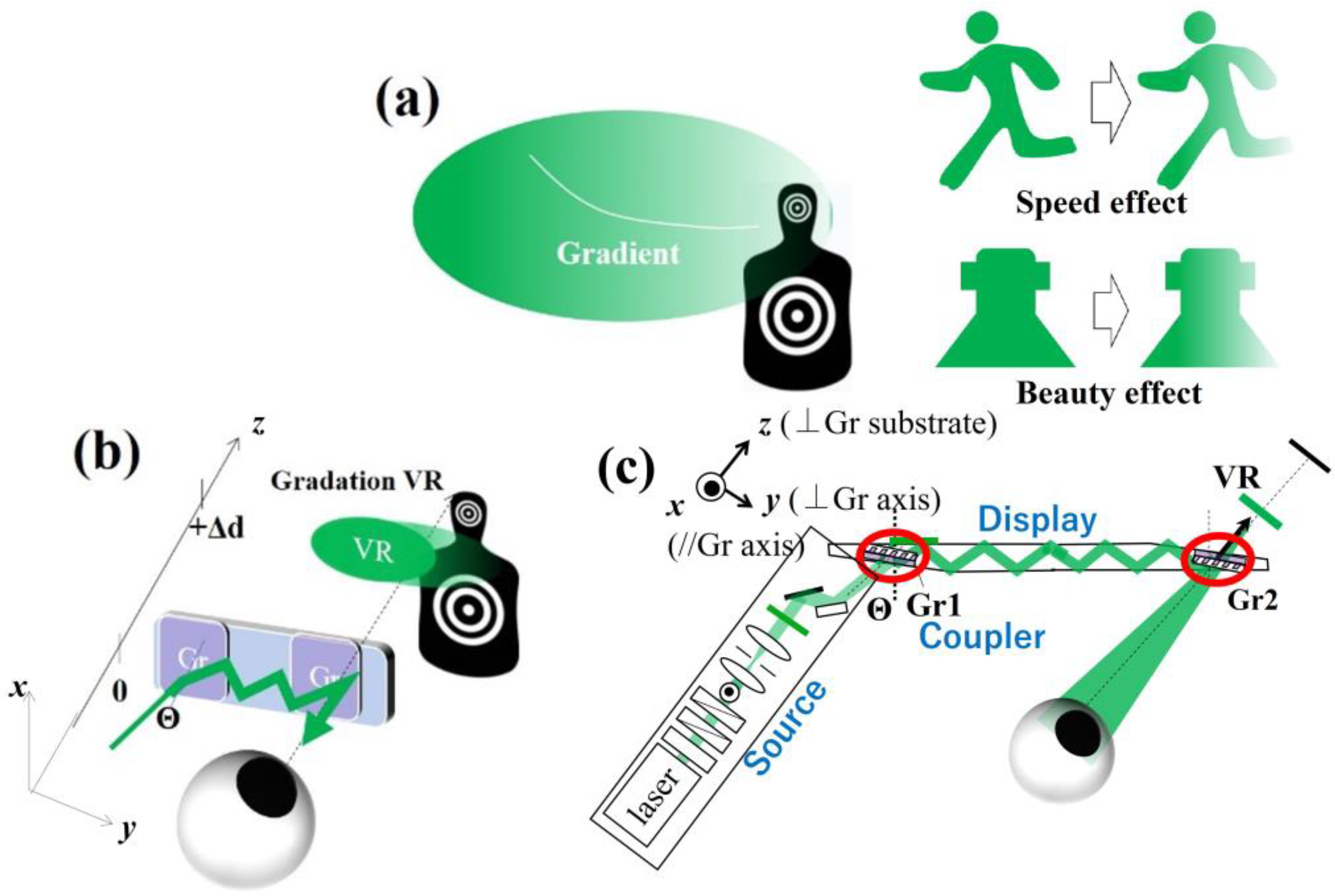
In this work, we focus on creating the gradation VR image on a waveguide HMD. The gradation VR is the phenomenon of the generated intensity gradient to a specific direction of a VR image (see Figure 1a). It can provide the user with the illusion of one-directional movement on a VR image. If this is applied in real space, users can feel as if they are moving as ghosts. The realization of this phenomena will provide users with a higher immersive sense. Hence, one candidate for application is the (speed)-illusion-effect-assisting [3] VR display, as illustrated in the upper right of Figure 1. By using this display, the VR image provides users with the speed illusion. This will be useful as a vehicle simulator and game. Another candidate is the beauty-effect-assisting [4] VR display, as illustrated in the center right of Figure 1. By giving off a lingering impression of beauty, the obtained cleanliness attracts the user. This will be useful in dressing rooms, for example, as users try on clothes.
In detail, to realize this, we attempted to duplicate multiple light source beams by using Guided Mode Resonance (GMR) [5,6,7,8,9] and then obtained the VR image with the above one-dimensional gradation. The GMR consists of a mixing mode of diffraction with a waveguide in a dielectric slab [5,6,7,8]. If the waveguide layer becomes thin, the number of optical collisions at the surface of the slab with optical absorbance should be increased slightly. The number of emission beams is secured sufficiently with this effect. As a result, the obtained emission beam is also likely to exhibit gradation image features, which can then also be used as VR images.
In this experiment, we investigated the resonance of the guided propagation mode generated in a SiO2-embedded-TiO2-slanted grating coupler [10,11], fabricated using electron beam lithography (EBL) [12], reactive ion etching (RIE) [12], and electron beam deposition (EBD) [13]. Specifically, we theoretically and experimentally investigated the guided mode resonance for incident angle resolution in the TiO2 layer. Resonance is generally acknowledged to be sensitive to the injection angle Θ in an optical leaky resonance mode [5]. Therefore, we first attempted to observe beams emitted from the grating sample at resonance by sweeping the incident angle Θ. The beam intensity enhanced (or attenuated) at resonance. Next, we confirmed the beams emitted on the grating coupler at resonance. The observed emission beam image provided the gradation on it. Furthermore, we confirmed the VR image converted by another grating coupler. The fabricated VR image was floating on air, and the image had short propagation (driving) features as well as emission beams. Finally, we fabricated a prototype of a wearable type of VR-HMD and observed the gradation VR images with the naked eye.
Figure 1b illustrates a 3D-viewer model that shows how users can see a VR image when they wear an HMD goggle with such a gradation effect. The beam created the gradation VR image through pair grating couplers, then the image was displayed through a waveguide glass in the user’s line of vision, which was overlapped with the target. The right side of an image is assumed to be the obtained VR image, exhibiting a weak intensity to recognize the target.
Figure 1c shows the entire configuration of a GMR-based VR-HMD fabricated by a SiO2-embedded-TiO2-slanted nanograting coupler [10,11] using EBL, RIE, and EBD methods as a development objective. As a guided optical configuration, the transmission optical configuration was adopted, which is a convenient design for an HMD. In this case, optical transmittance at resonance generally should be attenuated. However, our sample had a complicated structure, so such a consideration for intensity attenuation was disregarded. In the optical path, the beam emitted from the light source was first diffracted at the input grating coupler (Gr1) through several optical elements. Then, beams were waveguided in the display (WG) with total internal reflection (TIR), after which they are re-diffracted at the output grating coupler (Gr2) and directed to the users’ eye, where they could view the virtual image on a target. Here, the observed gradation VR image was static. However, we assume that the gradation VR animation will be viewed on an HMD unit equipped with a projection device, such as a beam-steering device (BSD) or a spatial light modulator (SLM) [11] in front of the LS.
2. Theoretical Calculation
2.1. Calculation Model
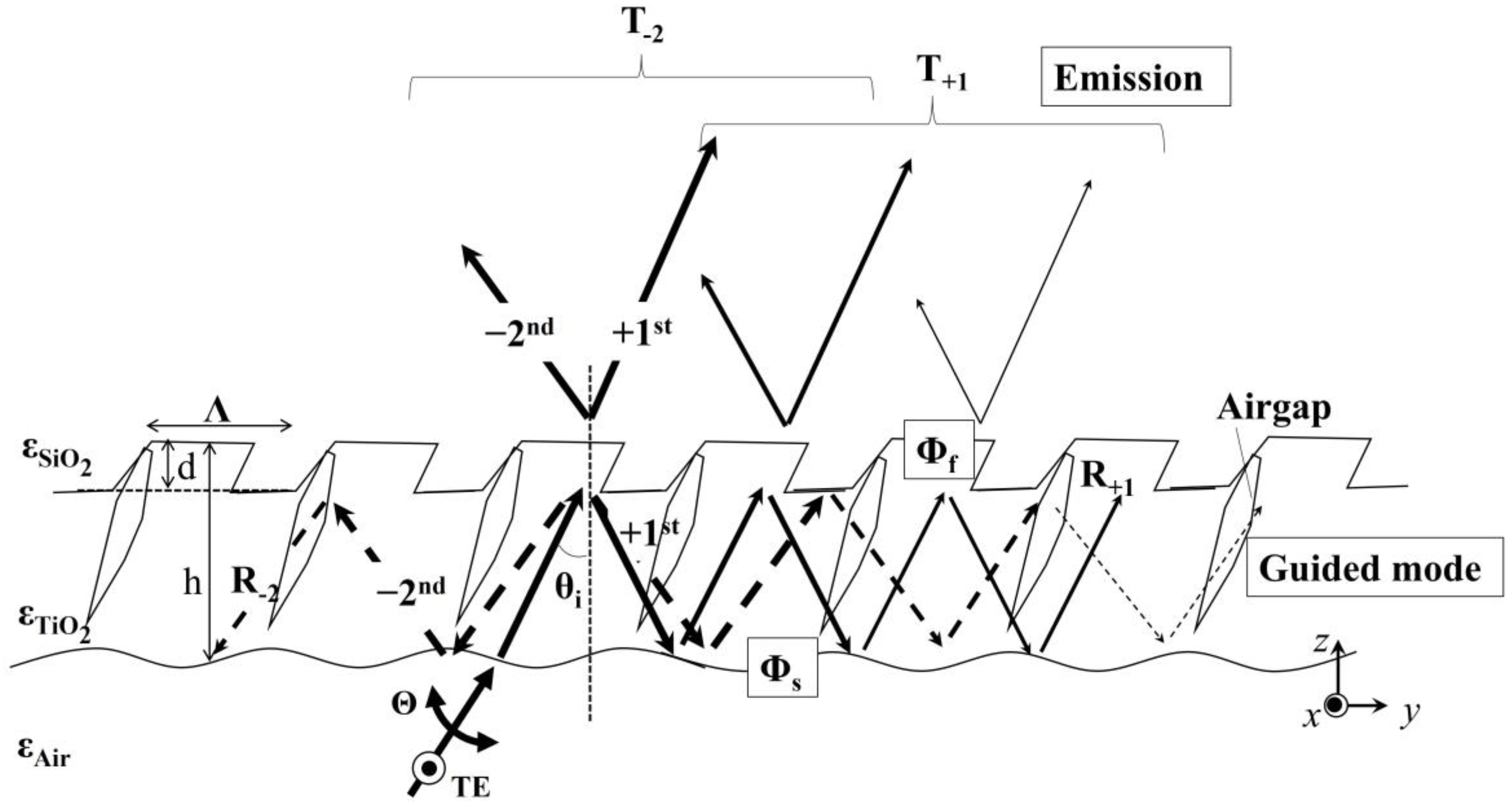
Figure 2 shows the theoretical model for the guided mode excitation on a cross section of the SiO2-embedded-TiO2-slanted grating sample that was fabricated previously. This is based on Ref. [8]. Here, directions for grating axis, beam propagation, and substrate normal axis are defined as x, y, and z, respectively. As illustrated in Figure 2, beam irradiated from the backside of the grating layer is high-order diffracted [14], and the waveguide exhibits a zigzag pattern in the TiO2 layer. Then, beams generating on the surface form beam aggregation. Therefore, the total electric fields E−2, E+1 for transmitted beams T−2, and T+1 are given as follows by adding the electric fields for the −2nd- and +1st-order diffraction rays [15] generated at the grating surface:
where
Here, N is the number of surface collisions; neff is the effective refractive index under the condition of a phase mismatch on the grating layer; and Φs and Φf are the phase mismatches generated at the back and front surfaces, respectively. The effective refractive index neff can be expressed as follows using the periodicity Λ, wavelength λ, and incident angle Θ:
From these equations, the intensity of the emitted beam E depends strongly on the incident angle Θ or wavelength λ. In this work, we focused on investigating the resonant angle Θres by sweeping Θ.
2.2. Field Calculation
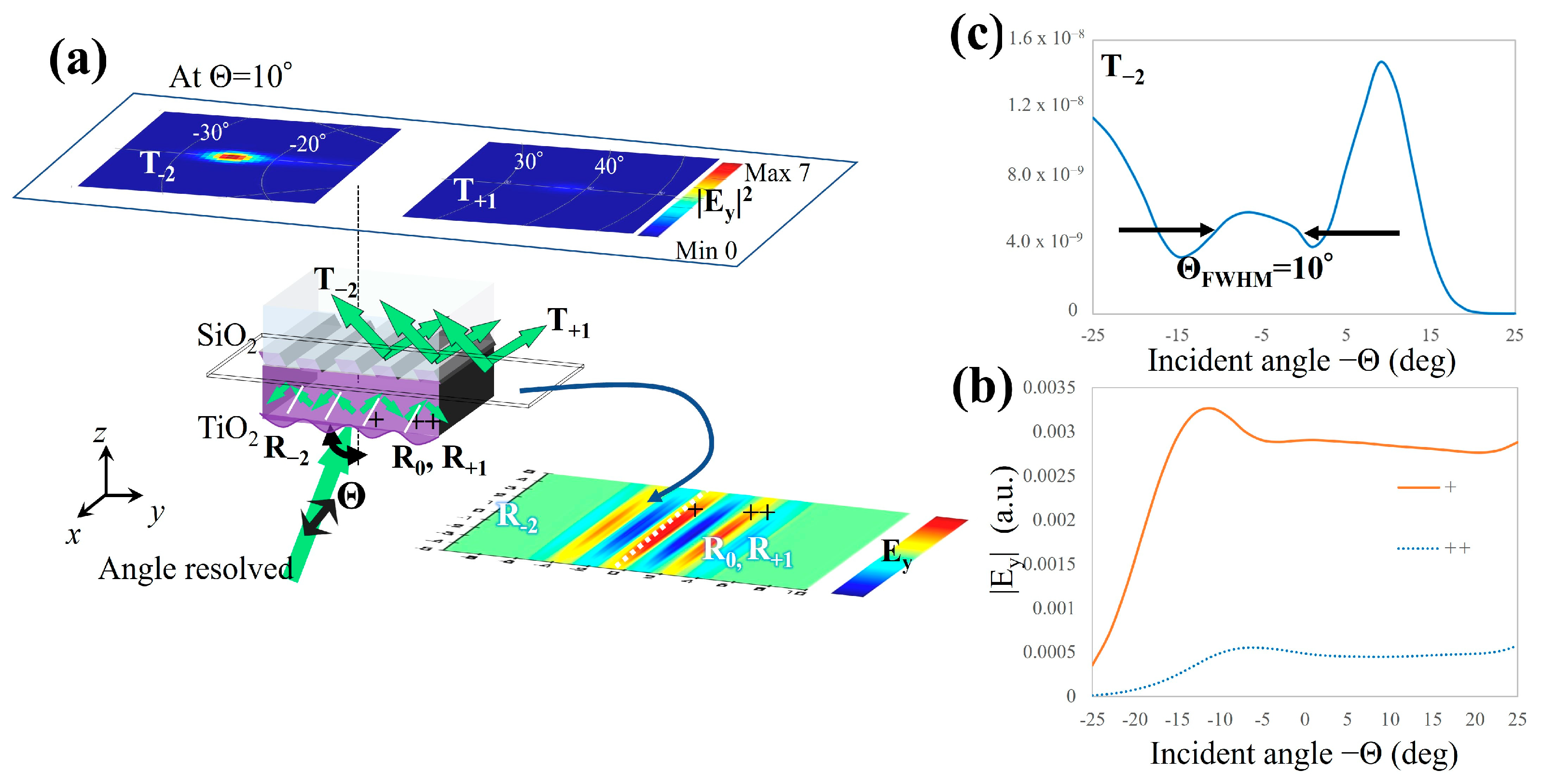
In addition, the electric field distribution for the cross section of the TiO2 dielectric layer was analyzed using finite-difference time-domain (FDTD) simulation software [5]. Figure 3a shows the optical configuration condition using the following parameter settings:—wavelength of injection beam: (λ) = 532 nm; polarization: TE; diameter: (D) = 5 μm; beam profile: Gaussian profile; simulation time: (t) = 25 fs; mesh step: (s) < 50 nm; and boundary conditions: perfect matching layer (PML). In the simulation, negative influences (e.g., air gaps and back side surface roughness) were also included.
First, we calculated the electric fields in the cross section of the TiO2 layer as a function of the incident angle Θ. As seen in the data in Figure 3a, it is anticipated that the presence of propagating waves in the thin layer of TiO2 at Θ = 10°. The right-hand side of Figure 3a shows the field profile of the cross section of the sample at resonance. Because the calculated electric fields showed a corrugated pattern composed of optical density at positive (+) and negative (−) for the edge side in the +y direction, we concluded that the guided wave was performed in a thin layer. Figure 3b shows the electric field of a cross section of the sample as a function of the incident angle Θ. We found not only the presence of strong guided mode excitation at resonant angle Θ = 10°, but also the change of field appeared between the + and ++ marked positions.
Next, far-field analysis was performed to verify the beam emissions in the guided resonance mode. As shown at the top of Figure 3a, we could verify the beam emissions composed of T−2 and T+1. These emission images had asymmetric intensity in the left and right, centered on the maximum field point. The emission intensity for T−2 at −25° was four times higher than that for T+1 at +38°. As seen in Figure 3c, an intensity peak of E−2 showed a maximum value at Θ = 9–10°. Hence, it is concluded that the hidden resonant angle Θres was deeply correlated with beam emission. In addition, we observed that the full width at half maximum (FWHM) for the intensity peak of |E−2| was ΘFHWM ≈ 10° at Θres = 9–10°, while total field for the emission beam was reduced in comparison with that at non-resonance.
3. Model for Waveguide Launcher
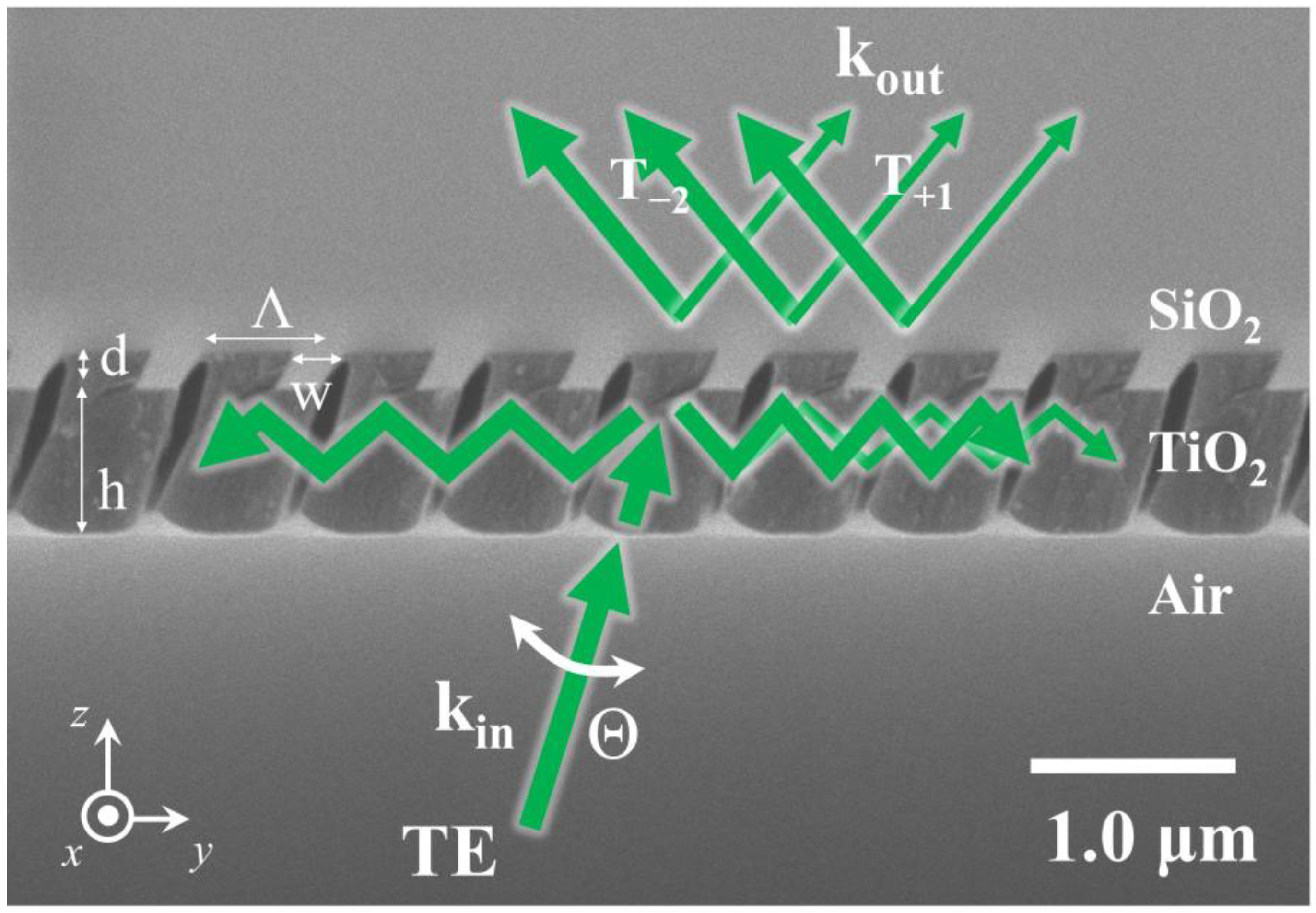
Figure 4 shows a scanning electron microscopy (SEM) image of the waveguide launcher consisting of the coupler sample that was fabricated previously [10,11]. In Figure 4, the wave vectors and waveguide patterns are indicated by arrows. Here, we explain the likely beam-duplication mechanism on the grating coupler. A resonance peak for the guided mode in the grating sample can be observed by sweeping a beam (kin) as a function of the incident angle Θ on the SiO2/TiO2 grating coupler. A layer of the resonant grating, as shown in Figure 4, is composed of −2nd- and +1st-order diffraction rays, leading to the formation of a zigzag waveguide lane. At the grating surface, the TiO2 layer formed a launcher to emit duplicate beams onto the SiO2 layer. That is, the waveguide beams passing through the grating could be emitted to the outside (kout). This was the mechanism for the twin waveguide beam launcher system. In this study, we investigated the emergence of a guided mode on an embedded grating.
4. Result and Discussion
4.1. Angle-Resolved Measurement
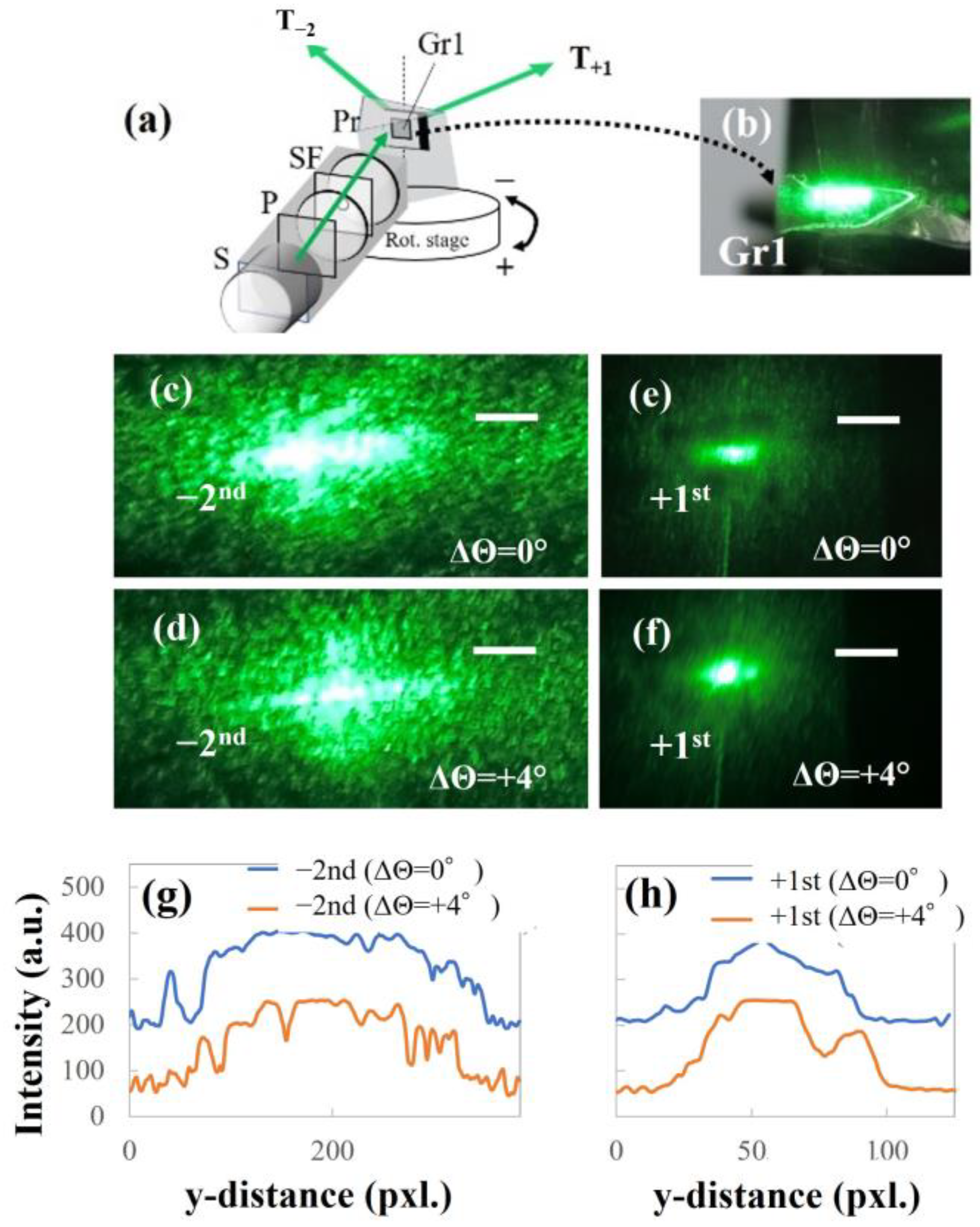
Figure 5a shows a diagram for the optical configuration of the incident angle-resolved measurements of the sample. Figure 5b shows a photo of the laser irradiation part of the input coupler sample. The transverse electric (TE) polarized beam with λ = 532 nm passed through the polarizer (P), aperture (AP), mirror (M), beam splitter (BS), spatial filter (SF), and prism (Pr). Then, the beam penetrated from the rear side of the grating (Gr) sample mounted on the Pr. The −2nd- and +1st-order diffraction rays should form zigzag waveguides consisting of multiple reflections in a TiO2 layer and permit the generation of propagation leakage to a SiO2 layer (i.e., leaky propagation); here, their beams can enable these to emit to the exterior of a SiO2 substrate as multiplication beams. In this experiment, we attempted to observe duplication beams with asymmetric intensity in the far field to verify the presence of leaky emission at the surface of the TiO2 layer.
Figure 5c–f show images for T−2 and T+1 of the −2nd- and +1st-order diffraction beam spots. Figure 5c–f show the photos of the −2nd- and +1st-order beam patterns at resonance Θ = 10° and non-resonance Θ = 14°, respectively. According to photo data (and power measurement data), it is clear that the diffraction intensity for −2nd-order is higher than that for +1st-order. These measurement data reproduced the simulation data well. On the other hand, any beam patterns indicating asymmetric intensity gradients on both sides of the waveguide direction are created, unless the aspect ratio of the diffraction image changes based on the theory of [19]. The detail originated from the negative intensity gradient to the waveguide direction induced by GMR.
Figure 5g,h show the intensity line profiles for gradation beam patterns at each order. From the data, we proved that the intensity pattern tilted to the right in both cases of the diffraction order. In addition, the intensity at Θ = 10° was smoother than that at Θ = 14°. This fact shows that the intensity pattern was sensitive to the change of injection angle Θ. In the next step, we analyzed the waveguide and emission using a display.
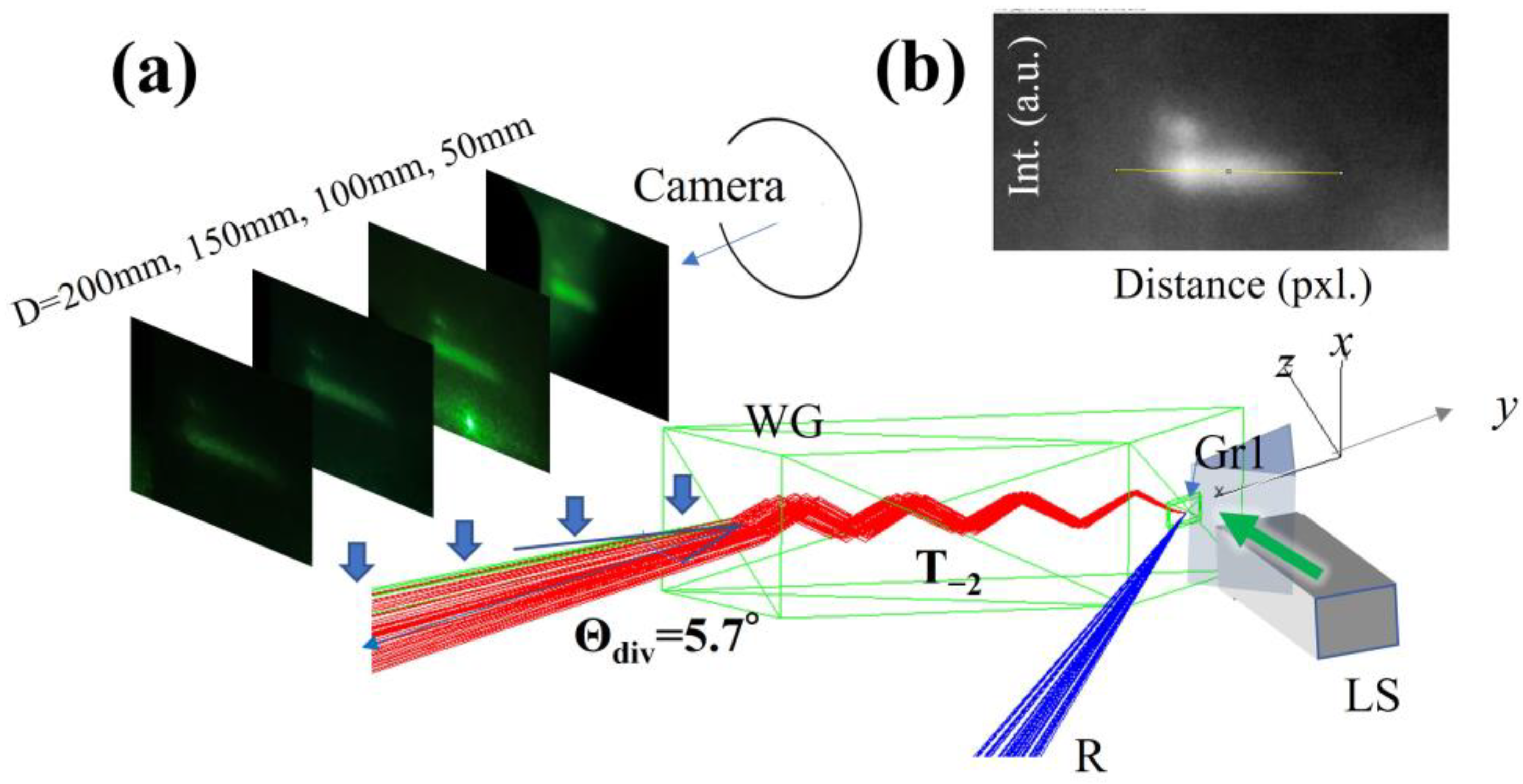
4.2. Beam Emission (on the Benchtop)
Figure 6a shows the ray-tracing simulation data for the beam emission of −2nd-order at Θ = 10° using TracePro software. As shown in Figure 6a, the ray-trace data reproduced the optical path [1] as “injection at LS ⇒ diffraction at Gr1 ⇒ TIR waveguide in WG”. When the beam was injected onto the Gr1 surface, it split into two. Then, the T−2 beam was emitted to the left direction and the beam for T+1 was emitted to the right direction. Thereafter, the T−2 beam was emitted from the side face of the WG. The experiment showed that the beam could be observed at different positions at D = 50, 100, 150, and 200 mm and was emitted from the side face of a WG, with a divergence angle of Θdiv = 5.7°.
4.3. VR Imaging (on the Benchtop)
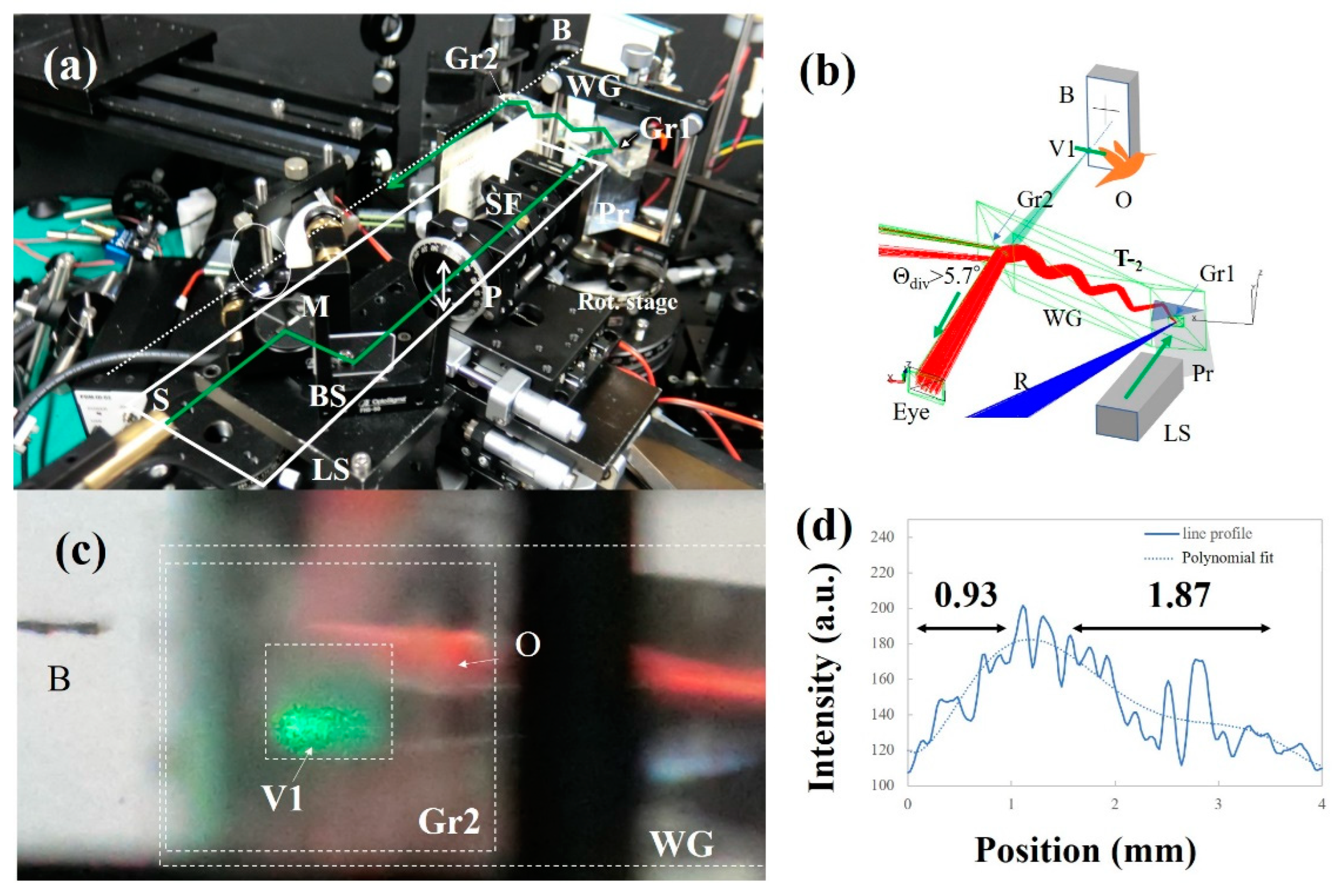
Figure 7 shows the test results for the VR-HMD imaging. We observed that a VR image developed over the WG by adding an output grating coupler (Gr2) on the opposite side of Gr1.
Figure 7a shows the final setup for VR imaging on the benchtop HMD. Furthermore, Figure 7b shows the result of the ray-tracing simulation for the HMD model. After the beam diffracted by Gr1 was guided by TIR in the WG, the diffracted beam was re-diffracted at Gr2 with a divergence angle Θdiv > 5.7°. Then, it was projected in front of an eye position corresponding to the position of the eye box. We set a camera at the eye position and then created the aerial VR image to the origami position (O) in front of the board position. We note that information for thin film waveguides was difficult to verify because the TracePro simulation software could not address microscopic data. Consequently, we verified that the waveguiding path for the VR imaging had been simulated effectively.
Figure 7c shows the VR image results. According to Figure 7c, a line-shaped aerial VR image with a sideband was observed. It was floating in the focal plane, similar to an origami object (O).
Figure 7d shows the horizontal line profile for the created gradation VR image. Edge responses for this VR image were determined to be 1/0.93 lines/mm (left side) and 1/1.87 lines/mm (right side). From these data, we concluded that the VR image had a short gradation for the right-hand side of the waveguide direction.
According to Refs. [20,21], efficiency, resolution, and field of view (fov) for VR images on waveguide HMD were, on average, ~40%, ~6.00 lines/mm, and ~15 deg (diagonal), respectively. According to Ref. [20], it was also reported that diffraction efficiency was enhanced by inserting an optical interlayer. As a result, the optical performance values obtained in this work (~30%, ~1.02 lines/mm, and 11.4 deg) were the same as the above-referenced values.
The obtained result proved that the gradation beam waveguided in a display was successfully converted to an aerial VR image. Such a VR image should be newly classified as structured VR light [22]. As for future applications, a portable device-assisted waveguide HMD is plausible; in particular, the fusion of a controller device used by a Wii and a wearable HMD device as fabricated in this work. If the behavior of the VR image is interlinked with the movement of the user’s hand equipped with a device, it can open up many interesting applications in the game and simulator fields. One interesting application would be changing the speed of the movement of a VR image between un-shaking and shaking movements of the hand. Concretely, there are two final applications for this device. One is the application as a real-time VR simulator. By demonstrating a relation between (1) the accelerator handgrip of a bike and an engine ignition on the VR, this can be attained. Another is the application to a VR game for entertainment. By demonstrating a relation between (2) the gear grip of a gas burner (or liter) and fluctuation of a flame, this can be attained. Applications such as these can create a new type of VR concept. Once we are able to reproduce such situations on this waveguide HMD, the immersive sense that users feel will be further enhanced.
5. Conclusions
In this work, we succeeded in creating the gradation (driving) VR pattern image emitted in two directions by using the SiO2-embedded-TiO2-slanted grating coupler. The mechanism for the gradation VR image appeared to be a multi-duplication of the VR image originating from guided mode resonance. At the resonance, the profile for the emission beam made a short gradation to become one-directional. Furthermore, the obtained gradation beam could be converted to a VR image by using a second coupler. These obtained gradation VR images were formed for −2nd- and +1st-order diffraction beams. In the future, the fabricated binocular waveguide HMD emitting gradation VR images have potential as speed-switching (2nd driving) HMD units by changing the incident angle Θ.
Funding
This research received no external funding.
Institutional Review Board Statement
Not applicable.
Informed Consent Statement
Informed consent was obtained from all subjects involved in the study.
Data Availability Statement
Data underlying the results presented in this paper are not publicly available at this time but may be obtained from the author upon reasonable request.
Acknowledgments
The author would like to thank Lumerical, Inc., and Lamda Research, Inc., for assisting with microscopic and macroscopic simulation techniques.
Conflicts of Interest
The authors declare no conflict of interest.
Appendix A
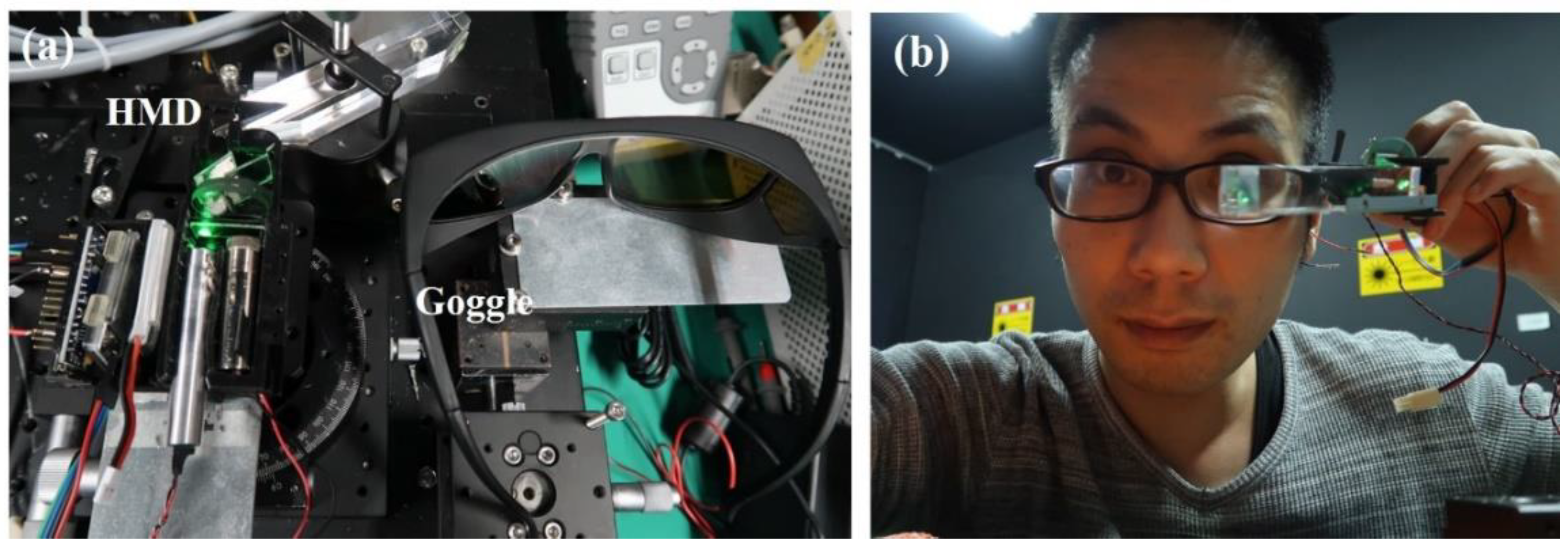
We transferred the VR-HMD from the benchtop type to the wearable type. Figure A1a shows the optical configuration for a wearable VR-HMD. The basic optical configuration is identical to the benchtop configuration. However, the entire length of the optical path is miniaturized to 170 × 150 × 30 mmt, which is considered to be an appropriate size for housing. In addition, the position of the eye box is adjusted on the basis of the assumption that it will be worn as an HMD, as seen in Figure A1b.
Figure A1.
(a) Overview of a wearable HMD device. (b) Photo of user (author) wearing the device.

References
- Liu, Z.; Pang, Y.; Pan, C.; Huang, Z. Design of a uniform-illumination binocular waveguide display with diffraction gratings and freeform optics. Opt. Express 2017, 25, 30720–30731. [Google Scholar] [CrossRef] [PubMed]
- Mattelin, M.A.; Radosavljevic, A.; Missinne, J.; Cuypers, D.; Steenberge, G.V. Design and fabrication of blazed gratings for a waveguide-type head mounted display. Opt. Exp. 2020, 28, 11175–11190. [Google Scholar] [CrossRef]
- Beatty, I.D. Standards-based grading in introductory university physics. J. Scholarsh. Teach. Learn. 2013, 13, 1–22. [Google Scholar]
- Available online: http://hdl.handle.net/11178/8212 (accessed on 1 March 2022).
- Zhou, Y.; Wang, B.; Guo, Z.; Wu, X. Guided Mode Resonance Sensors with Optimized Figure of Merit. Nanomaterials 2019, 9, 837. [Google Scholar] [CrossRef]
- Simornova, T.; Fitio, V.; Sakhno, O.; Yezhov, P.; Bendziak, A.; Hryn, V.; Bellucci, S. Resonant and Sensing Performance of Volume Waveguide Structures Based on Polymer Nanomaterials. Nanomaterials 2020, 10, 2114. [Google Scholar] [CrossRef] [PubMed]
- Sarkar, S.; Poulose, S.; Sahoo, P.K.; Joseph, J. Flexible and stretchable guided-mode resonant optical sensor: Single-step fabrication on a surface engineered polydimethylsiloxane substrate. OSA Contin. 2018, 1, 1277–1286. [Google Scholar] [CrossRef]
- Sahoo, P.K.; Sarkar, S.; Joseph, J. High sensitivity guided-mode-resonance optical sensor employing phase detection. Sci. Rep. 2017, 7, 7607. [Google Scholar] [CrossRef]
- Sasaki, Y.; Ushioda, S. Guided-wave polaritons in thin films of the layered compound GaSe. Phys. Rev. B 1983, 27, 1122. [Google Scholar] [CrossRef]
- Ogata, Y.; Kolchiba, M. Side edge emission from a waveguide substrate. Appl. Opt. 2021, 60, 9668–9671. [Google Scholar] [CrossRef]
- Ogata, Y. Beam Duplicator Consisting of a Waveguide Coupler 3 and Display on a Head Mounted Display. e-J. Surf. Sci. Nanotechnol. 2022, 20, 42–50. [Google Scholar] [CrossRef]
- Bai, B.; Laukkanen, J.; Kuittinen, M.; Siitonen, S. Optimization of nonbinary slanted surface-relief gratings as high-efficiency broadband couplers for light guides. Appl. Opt. 2010, 49, 5454–5464. [Google Scholar] [CrossRef] [PubMed]
- Ogata, Y.; Mizutani, G. Control of cross-sections and optical nonlinearity of Pt nanowires and the roughness effect. Phys. Res. Int. 2012, 969835. [Google Scholar] [CrossRef]
- Rao, J.; Varlamov, S. Light trapping in thin film polycrystalline silicon solar cell using diffractive gratings. Energy Procedia 2013, 33, 129–136. [Google Scholar] [CrossRef]
- Lee, J.; Park, J.; Lee, M. Nanostructured TiO2 diffraction grating fabricated via imprinting and TiCl4 treatment. J. Mater. Chem. C 2014, 2, 981–985. [Google Scholar] [CrossRef]
- Podilchak, S.K.; Freundorfer, A.P.; Antar, Y.M.M. Planar Leaky-Wave Antenna Designs Offering Conical-Sector Beam Scanning and Broadside Radiation Using Surface-Wave Launchers. IEEE Antennas Wirel. Propag. Lett. 2008, 7, 155–158. [Google Scholar] [CrossRef]
- Comite, D.; Podilchak, S.K.; Baccarelli, P.; Burghignoli, P.; Galli, A.; Freundorfer, A.P.; Antar, Y.M. A Dual-Layer Planar Leaky-Wave Antenna Designed for Linear Scanning Through Broadside. IEEE Antennas Wirel. Propag. Lett. 2017, 16, 1106–1110. [Google Scholar] [CrossRef]
- Comite, D.; Podilchak, S.K.; Baccarelli, P. Analysis and Design of a Compact Leaky-Wave Antenna for Wide-Band Broadside Radiation. Sci. Rep. 2018, 8, 17741. [Google Scholar] [CrossRef]
- Ogata, Y.; Vorobyev, A.; Guo, C. Symmetry-sensitive plasmonic enhancement of nonlinear optical intensity in nano-micro hierarchical structures on silver. Surf. Int. Anal. 2016, 48, 1108–1113. [Google Scholar] [CrossRef]
- Lin, Y.; Xu, H.; Shi, R.; Lu, L.; Zhang, S.-T.; Li, D. Enhanced diffraction efficiency with angular selectivity by inserting an optical interlayer into a diffractive waveguide for augmented reality displays. Opt. Express 2022, 30, 31244–31255. [Google Scholar] [CrossRef]
- Han, W.; Jeon, J.-M.; Choi, M.-H.; Park, J.-H. Lightguide type Maxwellian near-eye display with enlarged horizontal field of view by optical reconfiguration of input image. J. Inf. Disp. 2022, 23, 201–211. [Google Scholar] [CrossRef]
- He, C.; Shen, Y.; Forbes, A. Towards higher-dimensional structured light. Light Sci. Appl. 2022, 11, 205. [Google Scholar] [CrossRef] [PubMed]
Figure 1.
(a) One-directional gradation image on VR. Upper and middle right inserts: illustrations of speed and beauty effects, respectively. (b) Three-dimensional viewer of a VR-HMD. 0—display position, Δd—distance from display to VR image position. (c) optical configuration for a VR-HMD. Block—light source, circle—coupler (Gr1 and Gr2—input and output couplers, respectively), polygon—waveguide glass. Coordinates for x, y, and z are defined as grating axis, waveguide direction, and view-guiding axis, respectively.

Figure 2.
Theoretical model under guided mode: T—transmission, R—reflection, Λ—periodicity of gratings, h—height, d—thickness of slants, Θ—incident angle, Φs and Φr—phase shifts in surface and originating from dielectric, respectively. Note that arrows of wave vectors for weak intensity beams are not illustrated to avoid misunderstanding of contents. There is an assumption that the sharpened angles at air gaps correspond to the angles between +1st- and 0th-order diffraction rays.

Figure 3.
Electric field simulation for guided mode: (a) Three-dimensional FDTD structure model for a guided mode. Bottom: field monitor for a cross section of a layer at R−2, R0, and R+1 position. Top: far-field monitor at –x direction 25° (−2nd) and +x direction +38° (+1st). (b) Field profile for a cross section of a layer: |Ey| field profile at + and ++. (c) Field profile for a far field: |Ey−2| at resonant angle Θres = 9°–10°. ΘFWHM is calculated to be 10°. Note that here + direction 8° indicates 0th-order transmission beam, and intensity level for —direction 2° (−1st) is below noise.

Figure 4.
Twin waveguide launcher model of the periodicity, height, width, slant angle of gratings, and thickness of TiO2 are Λ = 704 nm, d = 230 nm, w = 200 nm, and h = 920 nm, respectively.
Figure 4.
Twin waveguide launcher model of the periodicity, height, width, slant angle of gratings, and thickness of TiO2 are Λ = 704 nm, d = 230 nm, w = 200 nm, and h = 920 nm, respectively.

Figure 5.
Angle-resolved observation for leaky mode analysis. (a) Optical configuration and (b) surface of input coupler sample. (c–f) Observed images for beam spots at Θ = 10° and +14°. (c,d) −2nd- and (e,f) +1st-order diffraction beam spots at Θ = 10° and +14°. (g,h) Line profiles for −2nd- and +1st-order beams. Scale bar: 3 mm. P—polarizer, SF—spatial filter, Pr—prism.

Figure 6.
Beam emitter (benchtop): (a) ray-tracing simulation. Left side: photo stacking for emission beams in distance from side face of waveguide display D = 50–200 mm. (b) Two-dimensional intensity line profile for image of D = 150 mm. WG—waveguide display, Θdiv—divergence angle, LS—light source module.

Figure 7.
VR imaging on benchtop: (a) setup, (b) ray-tracing simulation data, (c) VR imaging test, and (d) horizontal line profile data needed to determine edge response (~resolution) on both sides of the VR image. V1—virtual image of gradation pattern, B—board, O—origami object, BS—beam splitter, Gr2—output grating, (Gr2 output coupler size was too large to diffract the waveguiding beam perfectly). The gradation VR image seen in (b) was also well reproduced on wearable device (See Appendix A).

Disclaimer/Publisher’s Note: The statements, opinions and data contained in all publications are solely those of the individual author(s) and contributor(s) and not of MDPI and/or the editor(s). MDPI and/or the editor(s) disclaim responsibility for any injury to people or property resulting from any ideas, methods, instructions or products referred to in the content. |
© 2023 by the author. Licensee MDPI, Basel, Switzerland. This article is an open access article distributed under the terms and conditions of the Creative Commons Attribution (CC BY) license (https://creativecommons.org/licenses/by/4.0/).
Share and Cite
MDPI and ACS Style
Ogata, Y. Drive Type Virtual Reality Image on a Head-Mounted Display. Coatings 2023, 13, 961. https://doi.org/10.3390/coatings13050961
AMA Style
Ogata Y. Drive Type Virtual Reality Image on a Head-Mounted Display. Coatings. 2023; 13(5):961. https://doi.org/10.3390/coatings13050961
Chicago/Turabian StyleOgata, Yoichi. 2023. "Drive Type Virtual Reality Image on a Head-Mounted Display" Coatings 13, no. 5: 961. https://doi.org/10.3390/coatings13050961
Note that from the first issue of 2016, this journal uses article numbers instead of page numbers. See further details here.