
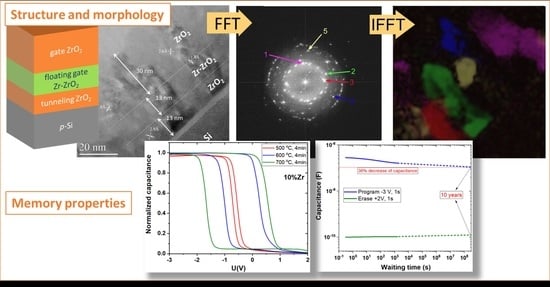
Memory Properties of Zr-Doped ZrO2 MOS-like Capacitor
 , , ,
, , , 
Abstract
:
1. Introduction
2. Materials and Methods
2.1. Sample Preparation
2.2. Characterization Methods
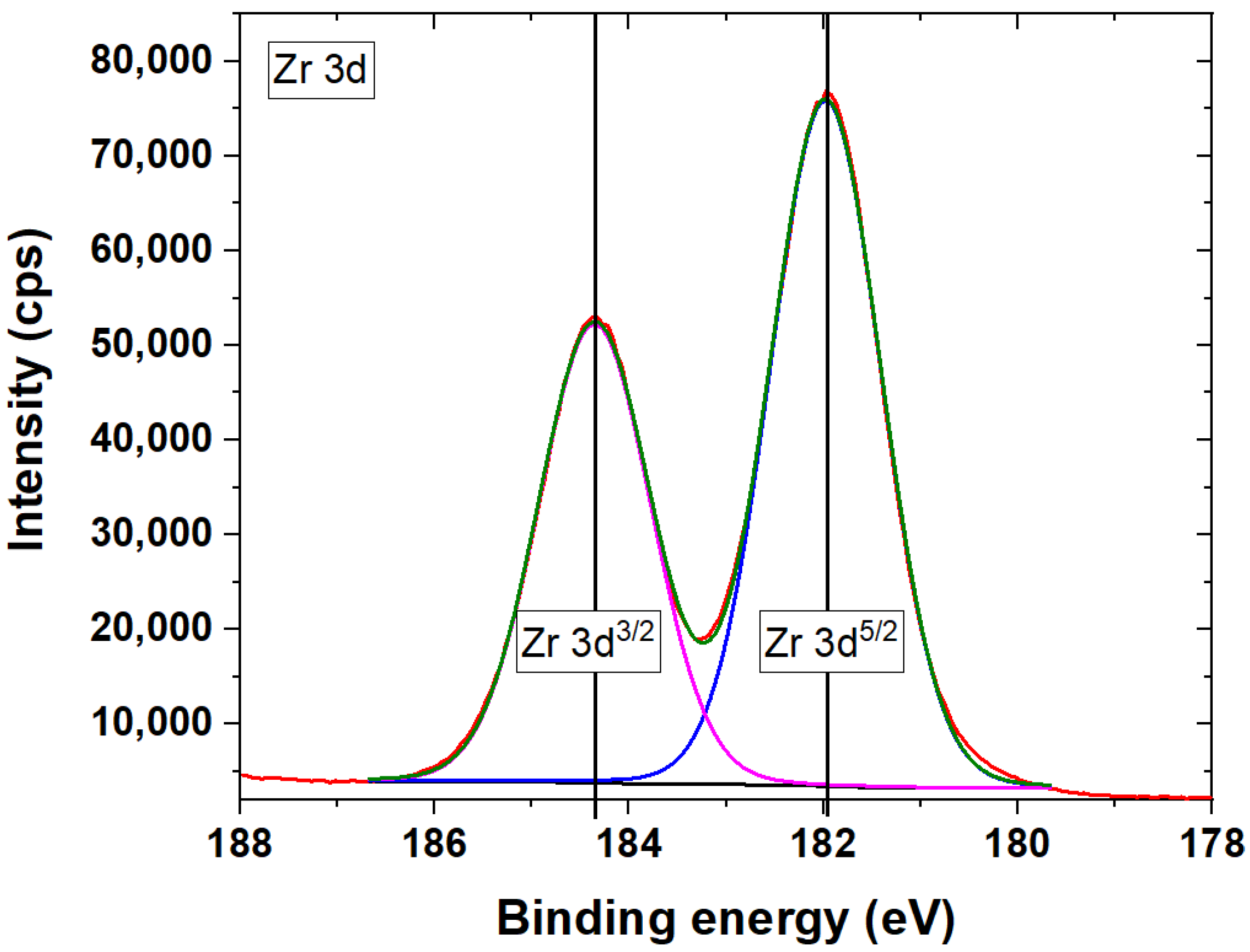
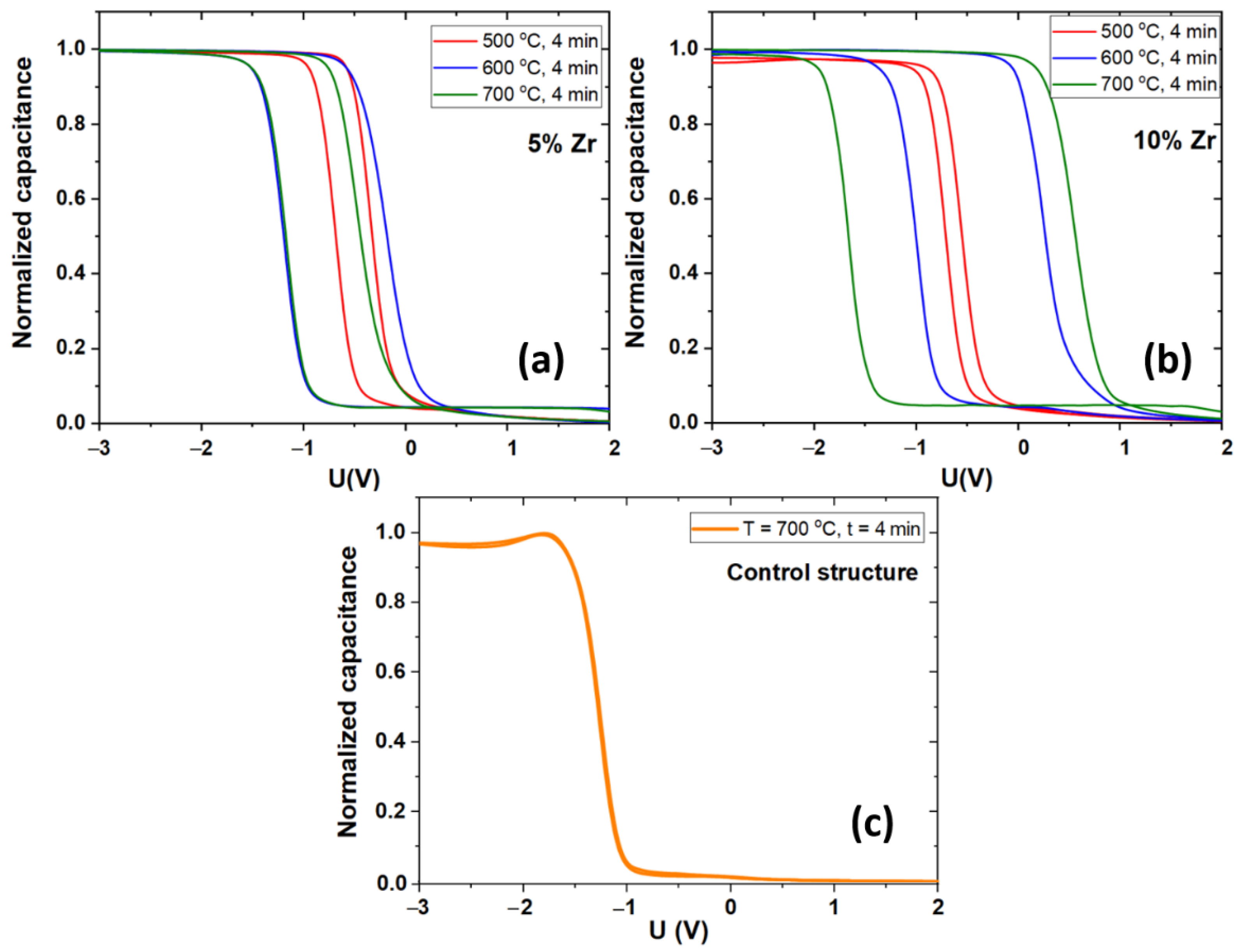
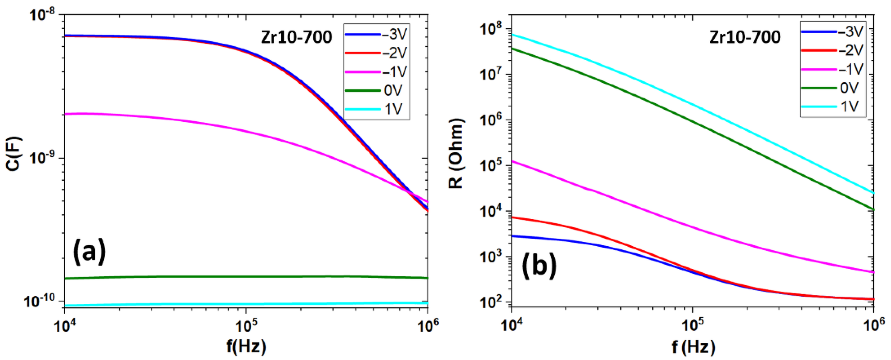
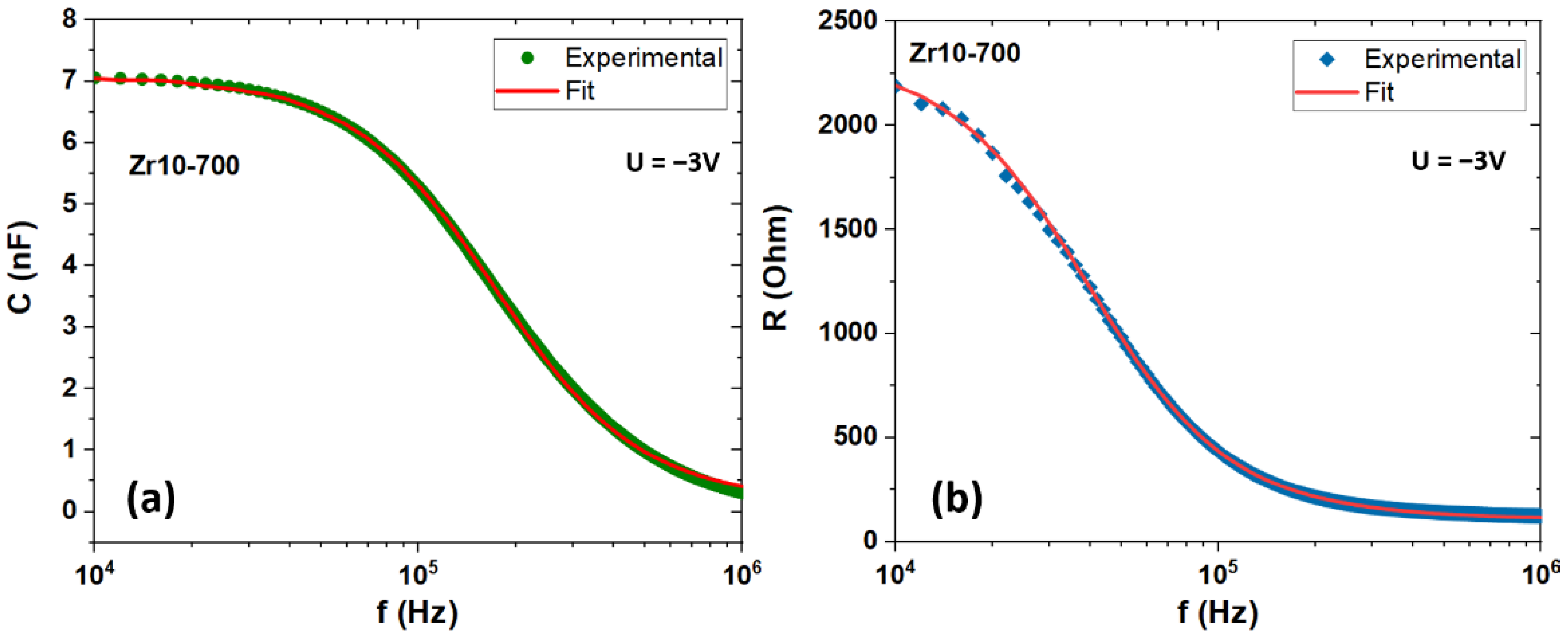
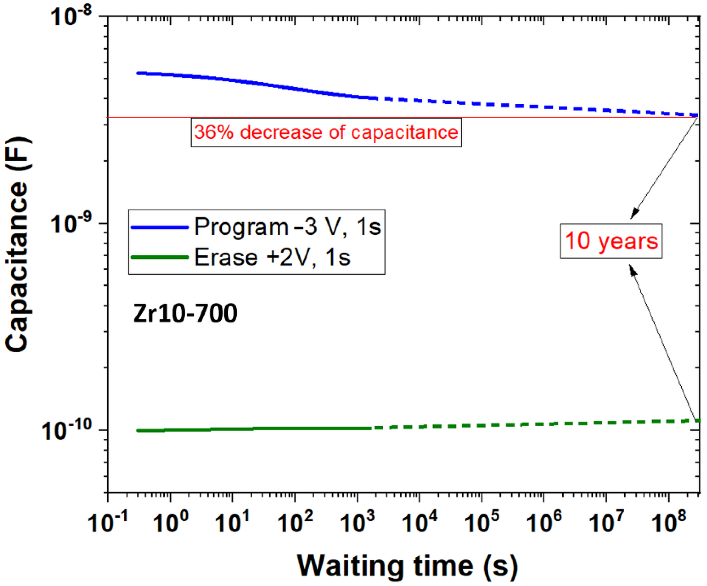
3. Results and Discussion
4. Conclusions
Author Contributions
Funding
Institutional Review Board Statement
Informed Consent Statement
Data Availability Statement
Conflicts of Interest
References
- Markov, S.; Sushko, P.V.; Roy, S.; Fiegna, C.; Sangiorgi, E.; Shluger, A.L.; Asenov, A. Si-SiO2 Interface Band-Gap Transition—Effects on MOS Inversion Layer. Phys. Status Solidi (a) 2008, 205, 1290–1295. [Google Scholar] [CrossRef]
- Kar, S.; Narasimhan, R.L. Characteristics of the Si-SiO2 Interface States in Thin (70–230 Å) Oxide Structures. J. Appl. Phys. 1987, 61, 5353–5359. [Google Scholar] [CrossRef]
- Majkusiak, B.; Walczak, J. Theoretical Limit for the SiO2 Thickness in Silicon MOS Devices. Sci. Technol. Semicond. Insul. Struct. Devices Oper. Harsh Environ. 2005, 185, 309–320. [Google Scholar] [CrossRef]
- Timp, G.; Bude, J.; Baumann, F.; Bourdelle, K.K.; Boone, T.; Garno, J.; Ghetti, A.; Green, M.; Gossmann, H.; Kim, Y.; et al. The Relentless March of the MOSFET Gate Oxide Thickness to Zero. Microelectron. Reliab. 2000, 40, 557–562. [Google Scholar] [CrossRef]
- Liu, J.; Li, J.; Wu, J.; Sun, J. Structure and Dielectric Property of High-k ZrO2 Films Grown by Atomic Layer Deposition Using Tetrakis (Dimethylamido) Zirconium and Ozone. Nanoscale Res. Lett. 2019, 14, 154. [Google Scholar] [CrossRef]
- Huang, K.-W.; Chang, T.-J.; Wang, C.-Y.; Yi, S.-H.; Wang, C.I.; Jiang, Y.-S.; Yin, Y.-T.; Lin, H.-C.; Chen, M.-J. Leakage Current Lowering and Film Densification of ZrO2 High-k Gate Dielectrics by Layer-By-Layer, In-Situ Atomic Layer Hydrogen Bombardment. Mater. Sci. Semicond. Processing 2020, 109, 104933. [Google Scholar] [CrossRef]
- Kashir, A.; Ghiasabadi Farahani, M.; Hwang, H. Towards an Ideal High-κ HfO2–ZrO2-Based Dielectric. Nanoscale 2021, 13, 13631–13640. [Google Scholar] [CrossRef]
- Palade, C.; Slav, A.; Cojocaru, O.; Teodorescu, V.S.; Stoica, T.; Ciurea, M.L.; Lepadatu, A.-M. SiGeSn Quantum Dots in HfO2 for Floating Gate Memory Capacitors. Coatings 2022, 12, 348. [Google Scholar] [CrossRef]
- Dragoman, M.; Dinescu, A.; Dragoman, D.; Palade, C.; Teodorescu, V.S.; Ciurea, M.L. Graphene/Ferroelectric (Ge-Doped HfO2) Adaptable Transistors Acting as Reconfigurable Logic Gates. Nanomaterials 2022, 12, 279. [Google Scholar] [CrossRef]
- Dragoman, M.; Dinescu, A.; Dragoman, D.; Palade, C.; Moldovan, A.; Dinescu, M.; Teodorescu, V.S.; Ciurea, M.L. Wafer-Scale Graphene-Ferroelectric HfO2/Ge–HfO2/HfO2 Transistors Acting as Three-Terminal Memristors. Nanotechnology 2020, 31, 495207. [Google Scholar] [CrossRef]
- Stavarache, I.; Cojocaru, O.; Maraloiu, V.A.; Teodorescu, V.S.; Stoica, T.; Ciurea, M.L. Effects of Ge-Related Storage Centers Formation in Al2O3 Enhancing the Performance of Floating Gate Memories. Appl. Surf. Sci. 2021, 542, 148702. [Google Scholar] [CrossRef]
- Ni, K.; Saha, A.; Chakraborty, W.; Ye, H.; Grisafe, B.; Smith, J.; Rayner, G.B.; Gupta, S.; Datta, S. Equivalent Oxide Thickness (EOT) Scaling with Hafnium Zirconium Oxide High-κ Dielectric near Morphotropic Phase Boundary. In Proceedings of the 2019 IEEE International Electron Devices Meeting (IEDM), San Francisco, CA, USA, 7–11 December 2019. [Google Scholar] [CrossRef]
- Zhao, H.; Yeo, Y.-C.; Rustagi, S.C.; Samudra, G.S. Analysis of the Effects of Fringing Electric Field on FinFET Device Performance and Structural Optimization Using 3-D Simulation. IEEE Trans. Electron. Devices 2008, 55, 1177–1184. [Google Scholar] [CrossRef]
- Yang, C.-F.; Hwu, J.-G. Role of Fringing Field on the Electrical Characteristics of Metal-Oxide-Semiconductor Capacitors with Co-Planar and Edge-Removed Oxides. AIP Adv. 2016, 6, 125017. [Google Scholar] [CrossRef]
- Peacock, P.W.; Xiong, K.; Tse, K.; Robertson, J. Bonding and Interface States of Si:HfO2 and Si:ZrO2 Interfaces. Phys. Rev. B 2006, 73, 075328. [Google Scholar] [CrossRef]
- Namavar, F.; Wang, G.; Cheung, C.L.; Sabirianov, R.F.; Zeng, X.C.; Mei, W.N.; Bai, J.; Brewer, J.R.; Haider, H.; Garvin, K.L. Thermal Stability of Nanostructurally Stabilized Zirconium Oxide. Nanotechnology 2007, 18, 415702. [Google Scholar] [CrossRef]
- Zhang, Y.; Zhang, J. First Principles Study of Structural and Thermodynamic Properties of Zirconia. Mater. Today Proc. 2014, 1, 44–54. [Google Scholar] [CrossRef]
- Haggerty, R.P.; Sarin, P.; Apostolov, Z.D.; Driemeyer, P.E.; Kriven, W.M. Thermal Expansion of HfO2 and ZrO2. J. Am. Ceram. Soc. 2014, 97, 2213–2222. [Google Scholar] [CrossRef]
- Panda, D.; Tseng, T.-Y. Growth, Dielectric Properties, and Memory Device Applications of ZrO2 Thin Films. Thin Solid Film. 2013, 531, 1–20. [Google Scholar] [CrossRef]
- Lehninger, D.; Khomenkova, L.; Röder, C.; Gärtner, G.; Abendroth, B.; Beyer, J.; Schneider, F.; Meyer, D.C.; Heitmann, J. Ge Nanostructures Embedded in ZrO2 Dielectric Films for Nonvolatile Memory Applications. ECS Trans. 2015, 66, 203–212. [Google Scholar] [CrossRef] [Green Version]
- Wu, Y.-H.; Wu, J.-R.; Wu, M.-L.; Chen, L.-L.; Lin, C.-C. Ge-Based Nonvolatile Memory Formed on Si Substrate with Ge-Stabilized Tetragonal ZrO2 as Charge Trapping Layer. J. Electrochem. Soc. 2011, 158, H410. [Google Scholar] [CrossRef]
- Palade, C.; Slav, A.; Ciurea, M.L. Memory Properties of GeZrO2 Based Trilayer Structure. In Proceedings of the 2021 International Semiconductor Conference (CAS), online, 6–8 October 2021. [Google Scholar] [CrossRef]
- Müller, J.; Böscke, T.S.; Schröder, U.; Mueller, S.; Bräuhaus, D.; Böttger, U.; Frey, L.; Mikolajick, T. Ferroelectricity in Simple Binary ZrO2 and HfO2. Nano Lett. 2012, 12, 4318–4323. [Google Scholar] [CrossRef] [PubMed]
- Li, Y.; Li, J.; Liang, R.; Zhao, R.; Xiong, B.; Liu, H.; Tian, H.; Yang, Y.; Ren, T.-L. Switching Dynamics of Ferroelectric HfO2-ZrO2 with Various ZrO2 Contents. Appl. Phys. Lett. 2019, 114, 142902. [Google Scholar] [CrossRef]
- Chen, Y.; Wang, L.; Liu, L.; Tang, L.; Yuan, X.; Chen, H.; Zhou, K.; Zhang, D. Thickness-Dependent Ferroelectric Properties of HfO2/ZrO2 Nanolaminates Using Atomic Layer Deposition. J. Mater. Sci. 2021, 56, 6064–6072. [Google Scholar] [CrossRef]
- Palade, C.; Lepadatu, A.-M.; Slav, A.; Cojocaru, O.; Iuga, A.; Maraloiu, V.A.; Moldovan, A.; Dinescu, M.; Teodorescu, V.S.; Stoica, T.; et al. A Nanoscale Continuous Transition from the Monoclinic to Ferroelectric Orthorhombic Phase inside HfO2 Nanocrystals Stabilized by HfO2 Capping and Self-Controlled Ge Doping. J. Mater. Chem. C 2021, 9, 12353–12366. [Google Scholar] [CrossRef]
- Lepadatu, A.M.; Palade, C.; Slav, A.; Maraloiu, A.V.; Lazanu, S.; Stoica, T.; Logofatu, C.; Teodorescu, V.S.; Ciurea, M.L. Single Layer of Ge Quantum Dots in HfO2 for Floating Gate Memory Capacitors. Nanotechnology 2017, 28, 175707. [Google Scholar] [CrossRef]
- Palade, C.; Lepadatu, A.M.; Slav, A.; Lazanu, S.; Teodorescu, V.S.; Stoica, T.; Ciurea, M.L. Material Parameters from Frequency Dispersion Simulation of Floating Gate Memory with Ge Nanocrystals in HfO2. Appl. Surf. Sci. 2018, 428, 698–702. [Google Scholar] [CrossRef]
- Hong, A.J.; Kim, J.; Kim, K.; Wang, Y.; Xiu, F.; Jeon, J.; Park, J.; Rauda, I.; Chen, L.-M.; Yang, Y.; et al. Cr Metal Thin Film Memory. J. Appl. Phys. 2011, 110, 054504. [Google Scholar] [CrossRef] [Green Version]


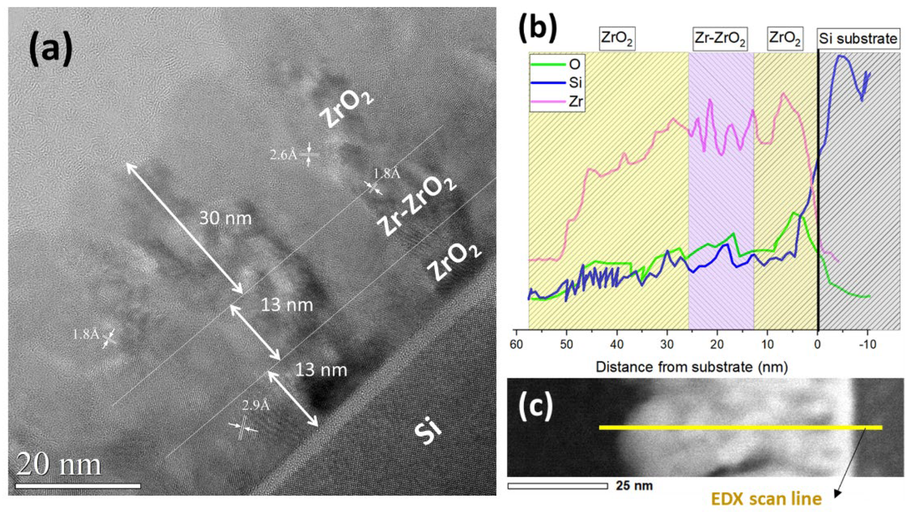
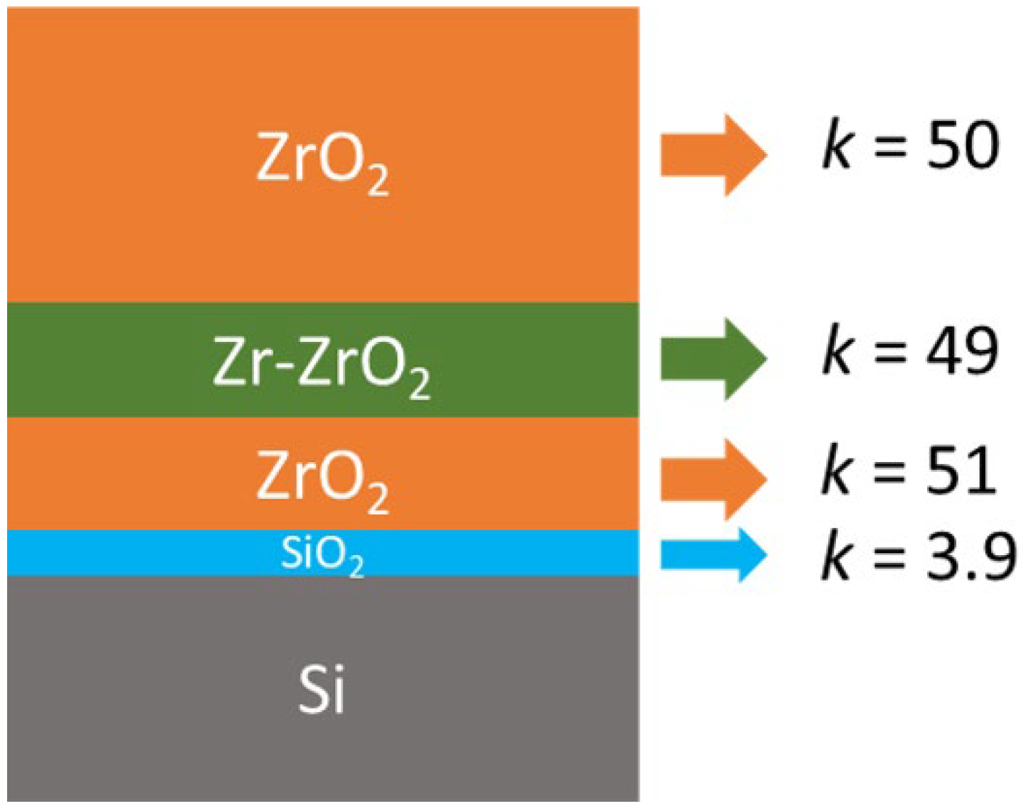
| Name | Floating Gate Layer Composition | Structure | Layers Thickness [nm] | Thermal Annealing | |
|---|---|---|---|---|---|
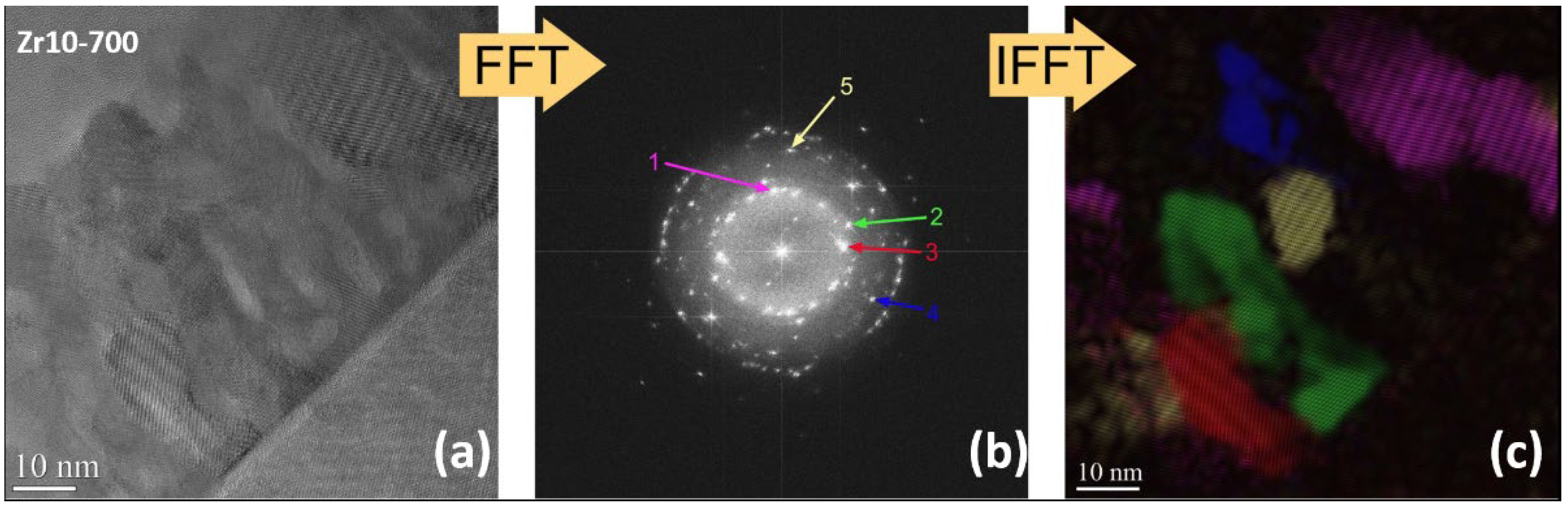
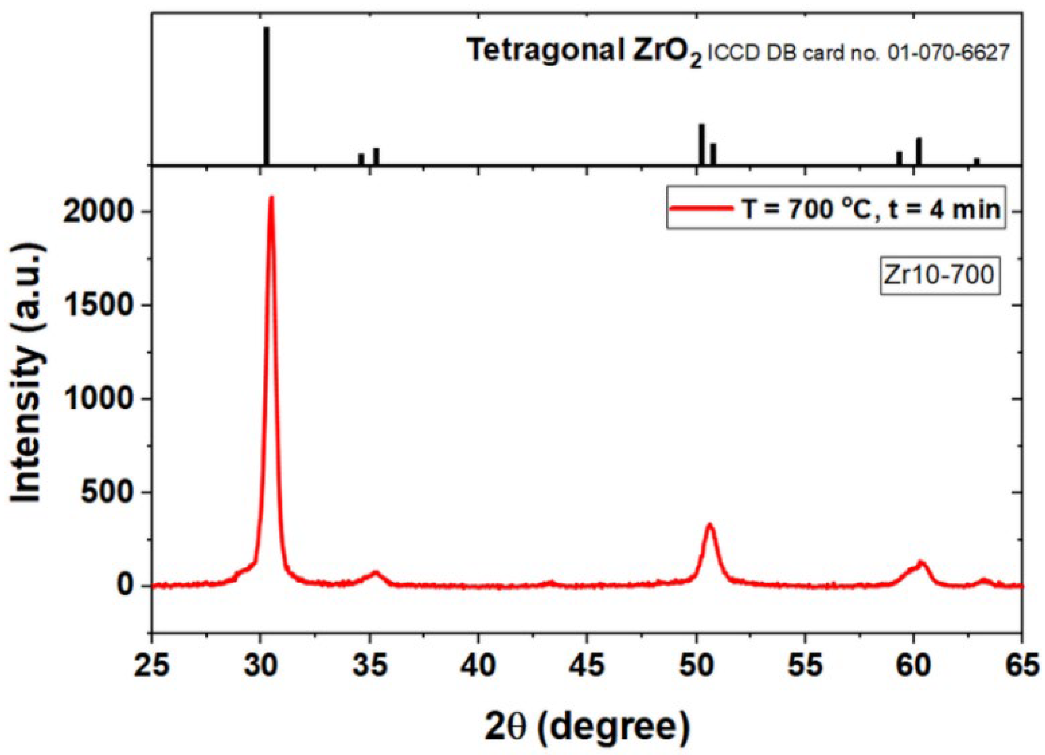
 | Zr5-500 Zr5-600 Zr5-700 | 5% Zr + 95% ZrO2 | ZrO2/Zr-ZrO2/ZrO 2/Si | 30/13/13 | T = 500 °C, t = 4 min T = 600 °C, t = 4 min T = 700 °C, t = 4 min |
| Zr10-500 Zr10-600 Zr10-700 | 10% Zr + 90% ZrO2 | ||||
 | Control | - | ZrO 2/Si | 56 | T = 700 °C, t = 4 min |
Publisher’s Note: MDPI stays neutral with regard to jurisdictional claims in published maps and institutional affiliations. |
© 2022 by the authors. Licensee MDPI, Basel, Switzerland. This article is an open access article distributed under the terms and conditions of the Creative Commons Attribution (CC BY) license (https://creativecommons.org/licenses/by/4.0/).
Share and Cite
Palade, C.; Slav, A.; Stavarache, I.; Maraloiu, V.A.; Negrila, C.; Ciurea, M.L. Memory Properties of Zr-Doped ZrO2 MOS-like Capacitor. Coatings 2022, 12, 1369. https://doi.org/10.3390/coatings12091369
Palade C, Slav A, Stavarache I, Maraloiu VA, Negrila C, Ciurea ML. Memory Properties of Zr-Doped ZrO2 MOS-like Capacitor. Coatings. 2022; 12(9):1369. https://doi.org/10.3390/coatings12091369
Chicago/Turabian StylePalade, Catalin, Adrian Slav, Ionel Stavarache, Valentin Adrian Maraloiu, Catalin Negrila, and Magdalena Lidia Ciurea. 2022. "Memory Properties of Zr-Doped ZrO2 MOS-like Capacitor" Coatings 12, no. 9: 1369. https://doi.org/10.3390/coatings12091369